Note: Descriptions are shown in the official language in which they were submitted.
CA 02665036 2012-08-15
74769-2376
CONTENT ADDRESSABLE MEMORY
Field of Disclosure
[0001] The present disclosure relates generally to memory architecture, and
more
specifically, to methods and systems for content addressable memory (CAM).
Background
[00021 CAMs can include conventional semiconductor memory (e.g., static random
access memory (SRAM)) and comparison circuitry that enables a search operation
to be
completed rapidly (e.g., in a single clock cycle). This ability allows
hardware
implementation of search algorithms, which provide greater speed than software
implemented searches. In a physical design of a CAM array structure, it is
desirable to
have a regular shape, such as a rectangle, in order to reduce the size. of the
CAM array
structure and make efficient use of space. Speed and power consumption are
issues in
high performance designs that are addressed by avoiding unnecessary parasitic
capacitance. A physical layout that reduces critical area and routing reduces
parasitic
capacitance.. However, certain aspects of CAM designs make achieving maximum
efficiency in their physical -design challenging.
[0003] FIG. 1 is a conceptual top level cache block diagram 100 of CAM 110 and
RAM
130 arrays having rows <0>, <1>, ... <n>. The CAM 110 and RAM 130 are
separated
by control circuit 120. As shown in FIG. 1, the CAM array 110 and the RAM
array 130
each have the same.number of rows. To produce an efficient design, it is
desirable to
match the CAM array 110 row height to the RAM array 130 row height, as shown
in
FIG. 1, so that the overall shape of the CAM array has a rectangular shape,
when
viewed in the x and y plane (i.e., the footprint of the RAM array), thereby
making
CA 02665036 2009-03-31
WO 2008/064172 PCT/US2007/085129
070485
2
efficient use of the area used. For purposes of this disclosure, the "row
height" refers to
the distance in the y-direction, as shown, for example, in FIG. 1.
[0004] In a static random access memory (SRAM) design, a 6-T storage cell
often
defines the minimum possible row height of the array structure. This RAM cell
is given
special ground rule waivers from a foundry so that process technologies can be
pushed
to the limit to produce a minimum area cell. FIG. 2A is a schematic of a
conventional
RAM array cell 200 which is composed of a 6-T storage cell. FIG. 2B shows a
RAM
array cell layout. Generally, the RAM cell 201 is provided by the foundry.
Significant
design effort is applied to reduce the physical size of the RAM cell and
thereby make
efficient use of the area used per cell, as shown in FIGS. 1 and 2B. Further,
when
designing the CAM array 110, the area on the CAM side (i.e., CAM array 110 in
FIG.
1) should also be reduced because it is desirable to obtain a one-to-one
correspondence
between the height of the CAM array 110 side and the RAM array 130 side.
[0005] With reference again to FIG. 1, a content addressable memory (CAM)
array 110
typically includes a storage cell, such as the 6-T RAM cell 201, and compare
circuitry
for each bit in the array. To produce an efficient design, it is desirable to
at least
substantially match the CAM array 110 row height to the RAM array 130 row
height
such that there is generally a one-to-one correspondence of the CAM array 110
and the
RAM array 130.
[0006] For example. one way to match the CAM array 110 row height to the RAM
array 130 row height is to limit the height of the CAM cells to the height of
the RAM
cell 201 which is included therein. Accordingly, there is a one-to-one
correspondence
in height between the height of each row of the CAM array 110 and each row of
the
RAM array 130, as shown in FIG. 1.
[0007] FIG. 3 shows one conventional way of implementing a matched row height
cache design. Particularly, FIG. 3 shows a non-interleaved set CAM array cell
layout
300 in which the height of the compare stacks 310 and 320 matches the height
of the
storage cell (i.e., RAM array cell 301). In the conventional designs, to
maintain the
common height, the nodes 315 and 316, which can be coupled to a matchline, are
split
up on either side of the cell, which results in additional capacitance.
[0008] In FIG. 3, the storage cell, i.e., RAM array cell 301, is laid out such
that two
compare stacks 310 (false/compliment) and 320 (true), are on each side of the
RAM
array ce11301. The row height of each of the compare stacks 310 and 320 is
designed to
CA 02665036 2009-03-31
WO 2008/064172 PCT/US2007/085129
070485
3
be no larger than the row height of the RAM array cell 301. The nodes 315 and
316 can
be connected by a net. For purposes of this disclosure, a net is a wire
connecting two or
more nodes (two or more points). When rows are stacked sequentially, as in
FIG. 3, and
compare lines are vertically aligned, significant capacitance is added to the
nodes 315,
316. The matchline nets are connected across each bit within a row, but may be
unique
from row to row, as illustrated in FIG. 4.
[0009] FIG.4 is an illustration of a conventional CAM design 400 in which rows
within
an array are placed consecutively. Each CAM array cell is identified by dashed
lines.
In FIG. 4, the compare lines are vertically aligned. However, in FIG. 4, the
compare
transistor stacks each have their own matchline, which results in increased
capacitance.
That is, in FIG. 4, the matchlines do not share diffusion.
[0010] As described above, the conventional CAM array designs, for example, as
shown in FIGS. 3 and 4, result in increased capacitance which degrades the
performance of the memory array. Thus, there is a need for a CAM array design
that
makes efficient use of space, reduces critical area and routing, and reduces
parasitic
capacitance.
SUMMARY
[0011] Exemplary embodiments of the invention are directed to systems and
methods
for Content Addressable Memory (CAM).
[0012] For example, an exemplary embodiment is directed to Content Adressable
Memory (CAM) including a first CAM cell having a first storage circuit and a
first
compare circuit, and a second CAM cell having a second storage circuit and a
second
compare circuit. The first CAM cell and the second CAM cell are positioned
into a
substantially rectangular area. The first and second storage circuits are
vertically
stacked. The first and second compare circuits are each positioned at
respective outer
edges of the rectangle.
[0013] Another exemplary embodiment is directed to a processor having a
Content
Addressable Memory (CAM) array including a plurality of CAM cell units. Each
CAM
cell unit includes a first CAM cell having a first storage circuit and a first
compare
circuit, and a second CAM cell having a second storage circuit and a second
compare
circuit. Each CAM cell is configured in an L-shape and the first and second
CAM cells
are arranged in an interlocking configuration to form a substantially
rectangular shape.
CA 02665036 2012-07-09
74769-2376
4
[0014] Another exemplary embodiment is directed to a method for producing a
Content Addressable Memory (CAM), including forming an L-shaped first CAM cell
having a first storage circuit and a first compare circuit, forming an L-
shaped second
CAM cell having a second storage circuit and a second compare circuit, and
arranging the first and second CAM cells in an interlocking configuration to
form a
substantially rectangular shape.
Another exemplary embodiment is directed to a Content Addressable
Memory (CAM) comprising: a first CAM cell having a first storage circuit and a
first
compare circuit, and a second CAM cell having a second storage circuit and a
second compare circuit, wherein the first CAM cell and the second CAM cell are
arranged in an interlocking configuration, such that they are positioned into
a
substantially rectangular area, wherein the first and second storage circuits
are
vertically stacked and adjacent to each other, and wherein the first and
second
compare circuits are separated by the first and second storage circuits, and
each
positioned at respective outer edges of the substantially rectangular area.
Another exemplary embodiment is directed to a processor having a
Content Addressable Memory (CAM) array, comprising: a plurality of CAM cell
units,
each CAM cell unit including: a first CAM cell having a first storage circuit
and a first
compare circuit; and a second CAM cell having a second storage circuit and a
second compare circuit, wherein each CAM cell is configured in an L-shape, and
wherein the first and second CAM cells are arranged in an interlocking
configuration
to form a substantially rectangular shape and wherein the first and second
storage
circuits are adjacent to each other and the first and second compare circuits
are
separated by the first and second storage circuits, and each compare circuit
is
positioned at respective outer edges of the rectangular area.
CA 02665036 2012-07-09
74769-2376
4a
Another exemplary embodiment is directed to a method for producing a
Content Addressable Memory (CAM), the method comprising: forming an L-shaped
first CAM cell having a first storage circuit and a first compare circuit;
forming an
L-shaped second CAM cell having a second storage circuit and a second compare
circuit; arranging the first and second CAM cells in an interlocking
configuration to
form a substantially rectangular shape; stacking the first and second storage
circuits
vertically and adjacent to each other; and positioning the first and second
compare
circuits are at respective outer edges of the substantially rectangular shape,
such that
they are separated by the first and second storage circuits.
CA 02665036 2012-07-09
74769-2376
4b
BRIEF DESCRIPTION OF THE DRAWINGS
[0015] The accompanying drawings are presented to aid in the description of
embodiments of the invention and are provided solely for illustration of the
embodiments and not limitation thereof.
[0016] FIG. 1 is a conceptual top level cache block diagram illustrating a CAM
and
RAM array.
[0017] FIG. 2A is a schematic illustrating a RAM array cell, and FIG. 2B is a
RAM
array cell layout.
[0018] FIG. 3 is an illustration of a non-interleaved set CAM array cell
layout.
[0019] FIG.4 is an illustration of a non-interleaved set scheme CAM design.
[0020] FIG. 5A is a schematic illustrating a CAM array cell, and FIG. 5B is a
CAM
array cell layout.
[0021] FIG. 6 is a block diagram illustrating a non-interleaved set scheme CAM
array.
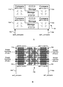
[0022] FIGs. 7A is a block diagram illustrating an interleaved CAM structure,
and FIG.
7B is a layout.of a set <0>, set<1> interleaved CAM structure.
[0023] FIG. 8 is an illustration of a block diagram illustrating an
interleaved 4-way set
associative CAM array bank.
[0024] FIG. 9 is an illustration of a diagram illustrating a direct mapped
decoder.
[0025] FIG. 10 is an illustration of a diagram illustrating a direct mapped
decoder for an
interleaved set cache.
DETAILED DESCRIPTION
[0026] Aspects of the invention are disclosed in the following description and
related
drawings directed to specific embodiments of the invention. Alternate
embodiments
may be devised without departing from the scope of the invention.
Additionally, well-
CA 02665036 2009-03-31
WO 2008/064172 PCT/US2007/085129
070485
known elements of the invention will not be described in detail or will be
omitted so as
not to obscure the relevant details of the invention.
[0027] The word "exemplary" is used herein to mean "serving as an example,
instance,
or illustration." Any embodiment described herein as "exemplary" is not
necessarily to
be construed as preferred or advantageous over other embodiments. Likewise,
the term
"embodiments of the invention" does not require that all embodiments of the
invention
include the discussed feature, advantage or mode of operation.
[0028] Embodiments of the invention relate generally to content addressable
memory
(CAM) structures, and more specifically, to methods and systems for providing
content
addressable memory (CAM) having a plurality of CAM cells (e.g., first and
second
CAM cells) arranged to reduce the area used and routing complexity, thereby
reducing
parasitic capacitance.
[0029] In one embodiment, matched CAM and RAM row heights are created by
rotating alternate CAM rows 180 relative to neighboring CAM rows, as shown,
for
example, in FIGS. 5 and 6, which will be described below in greater detail. It
is
desirable to avoid adding complicated routing requirements and significant
capacitance
that degrade design performance. Thus, another exemplary embodiment will be
described which applies an interleaved set scheme to provide a compacted
physical
placement with matched CAM and RAM row heights. According to an aspect of this
embodiment, the net capacitance is reduced through diffusion sharing while
maintaining
regular minimal signal routing. The exemplary embodiments reduce area, power
consumption, and increase maximum operating speed of the CAM design. Another
aspect of this embodiment is that it does not require a new decoding scheme. A
direct
mapped decoder is used by switching the input address bus order. Exemplary
aspects of
this embodiment will be described below with reference, for example, to FIGS.
7-10.
[0030] In one embodiment, the CAM array includes a 6-T storage cell 502, which
is
similar to the 6T storage cell illustrated in Fig. 2, and compare circuitry
505 for each bit
in the array, as shown in FIG. 5A. Regarding CAM array cell 500 performance,
the
node labeled matchline 510, in FIG. 5A, is one node that determines the CAM
search
performance. Therefore, it is desirable to reduce the capacitance on the
matchline node
510. Accordingly in at least one embodiment, the diffusion region of the
transistor
associated with compare complement /false (compare_c) is shared with diffusion
region
of the transistor associated with compare true (compare t) such that the
capacitance on
CA 02665036 2009-03-31
WO 2008/064172 PCT/US2007/085129
070485
6
the matchline node is reduced. Accordingly, by diffusion sharing and reducing
the
capacitance of the matchline, embodiments can reduce the power and increase
the
performance of the CAM array cell 500.
[0031] FIG. 5B is an illustration of a CAM array cell layout 501, according to
at least
one embodiment of the invention. Corresponding references, such as the
matchline
node 510, true T, complement C, compare true (compare_t), compare complement
/false
(compare_c), and Vss (vss_core), are provided for correlation to the schematic
diagram
of FIG 5A. As illustrated in FIG. 513, the layout of the CAM array cell 501
provides
greater diffusion sharing by providing adjacent compare circuitry 505 to
reduce
matchline capacitance by sharing a common matchline node 510 and diffusion
regions
of the adjacent transistors, as discussed in relation to FIG. 5A. Further,
embodiments
provide an `L' shaped cell (as indicated by the dashed lines) which has a
greater y
dimension than a conventional RAM array cell. That is, the height in the y-
direction of
the compare stack 505, as illustrated in FIG. 513, is greater than the height
in the y
direction of a conventional RAM array cell (see, e.g., FIG. 2B) or CAM cell
(see, e.g.,
FIG. 3).
[0032] With reference to FIG. 6, an embodiment of the invention can include a
non-
interleaved set scheme CAM array arranged in an interlocking `L' shape to
allow for
minimum area while providing the reduced matchline capacitance of the
embodiment of
FIG. 5B. FIG. 6 shows a CAM array 600 having CAM array cells 610, 620, 630,
and
640, each including a compare circuit and storage circuit (i.e., a RAM cell).
As
mentioned above, the layout of the CAM array cell is arranged to provide an
`L' shaped
cell which is taller than conventional RAM cells, but still allows for a
reduced area of
the memory array 600. Accordingly, each adjacent CAM array cell is rotated 180
relative to its neighbor to form the interlocking `L' shapes illustrated in
FIG. 6.
[0033] For example, CAM array cell 620 is rotated 180 relative to the CAM
array cell
610, and the CAM array cell 640 is rotated 180 relative to the CAM array cell
630.
Each interlocking `L' group provides for two storage cells and two compare
circuits.
The exemplary embodiment of FIG. 6 provides a compact design in which each
unit of
adjacent CAM array cells (e.g., 610 and 620, 630 and 640, etc.) forms a
rectangular
shape having a height that is substantially equal to twice the height of a
conventional
RAM array cell. Thus, the configuration of FIG. 6 provides a design that has
an overall
CA 02665036 2009-03-31
WO 2008/064172 PCT/US2007/085129
070485
7
one-to-one correspondence of RAM cell to compare cell, while providing reduced
matchline capacitance.
[0034] For purposes of this disclosure, stacking rotated rows sequentially
within a set
means that the compare inputs of every other row will be in a separate
vertical column.
The extra column of inputs results in two routing tracks per compare signal
(e.g.,
set-compare signal), as shown in FIG. 6. That is, if rotated rows are placed
in
sequential order within a set, there will be two routing tracks for each set
compare input
(e.g., set0_compare input 650 and 651, and setl_compare input 660 and 661);
one for
each vertical column. The extra column of inputs (e.g., 651 and 661) results
in
additional routing requirements.
[0035] To reduce the routing requirements and associated parasitic capacitance
with the
extra lines, an interleaved set scheme can be used according to embodiments of
the
invention. For example, as illustrated in FIG. 7A, an interleaved design also
has an
overall one-to-one correspondence between CAM and RAM row heights, while
reducing routing and parasitic capacitance. Net capacitance is reduced through
diffusion sharing while limiting or maintaining signal routing (e.g., regular
minimal
signal routing). The exemplary embodiments reduce area, power consumption, and
increase maximum operating speed of the CAM array. Also, at least one
exemplary
embodiment is implemented without requiring a new decoding scheme. In one
embodiment, a direct mapped decoder can be utilized by rearranging the input
address
bus order.
[0036] An interleaved set CAM, in one embodiment, uses a set associative array
design.
Instead of vertically placing sequential rows within a set, as illustrated in
FIG. 6, the
rows from two vertically adjacent sets are physically interleaved and the CAM
array
cells are rotated 180 relative to their neighbors. The interleaved pairs of
sets are
stacked vertically to populate each CAM bank. In at least one embodiment, set
specific
control signals within the CAM bank are in vertical alignment, such as
exemplarily
illustrated in FIG. 7A and 7B.
[0037] FIG. 7A is an illustration of a block diagram of an interleaved CAM
array 701.
The CAM array 701 has CAM cells 710, 720, 730, and 740, each including a
compare
circuit and a storage circuit (e.g., a SRAM cell). Each CAM array cell is
arranged to
provide an L-shaped cell which is greater in the y dimension than a
conventional RAM
cell. In order to reduce the area used by the design, each adjacent CAM array
cell is
CA 02665036 2009-03-31
WO 2008/064172 PCT/US2007/085129
070485
8
rotated 180 relative to that CAM cell's neighboring CAM cell. With reference
to FIG.
7A, the CAM cell 720 is rotated 180 relative to the CAM cell 710, and
arranged in an
interlocking `L' configuration. CAM array cell 740 is likewise rotated 180
relative to
the CAM array cell 730 in an interlocking `L' configuration, thereby providing
a
compact design in which each unit of adjacent CAM cells (e.g., 710 and 720,
730 and
740, etc.) forms a rectangular shape having a height that is equal to
approximately twice
the height of the storage cell (e.g., a SRAM cell). The interlocking
configuration of the
L-shaped CAM cells (e.g., 710 and 720) can be considered a CAM cell unit 705
and
CAM cell units can be stacked to form a CAM array such as illustrated in FIG.
8.
[00381 FIG. 7B is a circuit layout of an interleaved CAM structure 702. The
interleaved
sets, according to embodiments of the invention, produce CAM cells with
vertically
aligned set compare signals, reduce the parasitic capacitance, and lower power
consumption of the design. By interleaving sets, the set specific compare
signals (e.g.,
set0compare 750 and setl_compare 760) are vertically aligned. Further, since
one line
is used per compare component (e.g., compare true), the routing used for the
compare
lines is reduced. The two L-shaped cells share a matchline diffusion region as
discussed
above in relation to FIGs 5A and 5B. The resulting physical area of the array
and
capacitance in the design is reduced. Accordingly, embodiments of the
invention, such
as illustrated in FIGs. 7A and 7B, reduce both matchline and compare line
parasitic
capacitance.
[00391 Another embodiment will be described with reference to FIG. 8. FIG. 8
is an
interleaved 4-way set associative CAM array bank 800. In FIG. 8, there are
four rows
in each set (4-way) and each row is four bits wide (e.g., four columns).
Adjacent set
pairs are interleaved (set 0/set 1, set 2/set 3). Each CAM cell has an
associated set and
row and as previously discussed, each CAM cell unit has two CAM cells.
Accordingly
the CAM array 800 can be formed from a plurality of CAM cell units arranged to
correspond to a desired number of bits, sets, and rows. In the interleaved
design,
according to embodiments of the invention, each CAM cell unit has the same row
numbers but has sequential set numbers. For example, a CAM cell unit can have
a first
CAM cell with set <0>, row<0> and a second CAM cell with set <1>, row <0>.
When
arranged as illustrated in FIG. 8, a unique compare signal can be provided for
each bit
of each set. Further, the rows in a given bit and set (e.g., bit 0, set 0,
rows 1-4) receive
CA 02665036 2009-03-31
WO 2008/064172 PCT/US2007/085129
070485
9
the same bit level compare signals. Thus, the compare inputs of each row
within a set
are vertically aligned and coupled with one routing track per bit.
[0040] Other embodiments are directed to interleaved sets that are non-
adjacent sets. It
is noted that any two sets can be interleaved. In another embodiment, two
physically
adjacent sets, which are not logically adjacent, are interleaved. However,
embodiments
of the invention are not limited to 4-way set associative CAM arrays. Other
embodiments can be applied to other associative memory, such as 2-way, 16-way,
etc.
associative memories. Embodiments of the invention can take advantage of the
physical layout of the CAM cells to reduce the capacitance and improve the
performance in such associative memory arrays.
[0041] As discussed in the foregoing, an interleaved set scheme can be applied
to a
CAM array to provide a compact physical arrangement with an overall
correspondence
of CAM and RAM row heights (e.g., per two cells), while reducing or minimizing
routing and parasitic capacitance. Net capacitance is reduced through
diffusion sharing
while maintaining regular minimal (or reduced) signal routing. Accordingly,
embodiments of the invention reduce area, power consumption, and allow
increased
operating speed of a CAM design. Also, at least one embodiment is implemented
with
a direct mapped decoder.
[0042] FIG. 9 is an illustration of a direct mapped decoder 900. The direct
mapped
decoder 900 takes a 6-bit address and decodes to 64 outputs. Each output is
coupled to
one of 64 rows in a memory array or cache. For example, if logical address
bits A<5:0>
are coupled to decoder inputs a5-a0 as shown, the mapping correlates to a
physical
placement where sets and rows are placed sequentially. The cache has four sets
which
are mapped by logical address bits A<5> and A<4>. Each of the four sets has
sixteen
rows (i.e., rows 0-15, 16-31, 32-47, and 48-63) mapped by logical address bits
A<3:0>.
The direct mapped decoder 900 is designed for sequential row addresses.
However,
applying the direct mapping of the decoder 900 to the interleaved CAM array
would
result in complex routing of the decoder outputs.
[0043] FIG. 10 is an illustration of a block diagram of a direct mapped
decoder 1000
that can be used with an interleaved set CAM array in accordance with at least
one
embodiment of the invention. For example, the logical address bits A<5:0> can
be
reordered to correspond to the interleaved set CAM array. The logical address
bits
A<5:0> can be reordered and connected to decoder inputs a5-a0, as illustrated
in FIG.
CA 02665036 2009-03-31
WO 2008/064172 PCT/US2007/085129
070485
10. The mapping correlates to a physical placement where sets and rows are
placed
sequentially based on the interleaved set scheme. The cache has four sets
which are
mapped by logical address bits A<5> and A<4>. Each of the four sets has
sixteen rows
(i.e., rows 0-15, 16-31, 32-47, and 48-63) mapped by logical address bits
A<3:0>.
Logical address bit A<4> coupled to input a0. Logical address bits A<3:0> are
each
shifted left by one position to correspond to inputs a4-al, respectively.
Logical address
bit A<5> is coupled to input a5. For example, if logical address bits A<5:0>
are
coupled to decoder inputs a5-a0 as shown, the mapping correlates to a physical
placement having alternating sets, where rows stay the same for each group
(e.g., cell
unit) of alternating sets (e.g., set<0>,row<0>; set<l>,row<0>; set<0>,row<l>;
set<l>,row<l>; etc.). Therefore, the interleaved decoder 1000 of FIG. 10 can
directly
map to an interleaved set CAM array and does not result in complex routing of
the
decoder 1000 outputs. Thus, an exemplary embodiment interleaves the rows of
adjacent
sets and changes the order of the address bus connections to the decoder 1000
in order
to provide the correct mapping to the CAM array rows.
[0044] In other embodiments, a processor includes a CAM array according to the
embodiments described above. As used herein, a processor can include one or
more
processing circuits, for example, microprocessors, digital signal processors
(DSPs),
microcontrollers, Application Specific Integrated Circuits (ASICS) and
combinations
thereof. Accordingly, an embodiment can include a processor comprising a CAM
array
having a plurality of CAM cell units in which each CAM cell unit includes a
first CAM
cell having a first storage circuit and a first compare circuit, and a second
CAM cell
having a second storage circuit and a second compare circuit. Each CAM cell
can be
configured in an L-shape such that the first and second CAM cells are arranged
in an
interlocking configuration to form a substantially rectangular shape, thereby
minimizing
physical area of the array and/or the capacitance in the design. Accordingly,
the
embodiments described above can reduce both matchline and compare line
parasitic
capacitance in CAM array integrated within a processor.
[0045] Another embodiment is directed to a method of forming a CAM array, or a
processor including a CAM array having a plurality of CAM cells (e.g., first
and second
CAM cells) according to the embodiments described above, arranged to reduce
the area
used, routing complexity, and parasitic capacitance.
CA 02665036 2009-03-31
WO 2008/064172 PCT/US2007/085129
070485
11
[0046] For example, an embodiment is directed to a method having the steps of
forming
an L-shaped first CAM cell having a first storage circuit and a first compare
circuit, and
forming an L-shaped second CAM cell having a second storage circuit and a
second
compare circuit. The method includes arranging the first and second CAM cells
in an
interlocking configuration to form a substantially rectangular shape, in which
the first
and second storage circuits are vertically stacked, and the first and second
compare
circuits are each positioned at respective outer edges of the rectangle. The
method
further includes associating each CAM cell with a set and row.
[0047] For example, in one embodiment, the first CAM cell is associated with a
first
row of a first set and the second CAM cell is associated with a second row of
the first
set. The embodiment includes configuring a decoder to have sequential outputs
mapped
to the first row of the first set and to the second row of the first set.
[0048] In another embodiment, the first CAM cell is associated with a first
row of a first
set and the second CAM cell is associated with a first row of a second set.
The
embodiment includes configuring a decoder to have sequential outputs mapped to
the
first row of the first set and to the first row of the second set.
Accordingly, the
exemplary methods can provide a CAM array, or processor having a CAM array, in
which the physical area of the array and/or the capacitance can be reduced.
The
embodiments described above can reduce both matchline and compare line
parasitic
capacitance.
[0049] It should be appreciated that information and signals may be
represented using
any of a variety of different technologies and techniques. For example, data,
instructions, commands, information, signals, bits, symbols, and chips that
may be
referenced throughout the above description may be represented by voltages,
currents,
electromagnetic waves, magnetic fields or particles, optical fields or
particles, or any
combination thereof.
[0050] Further, it should be appreciated that the various illustrative logical
blocks,
modules, circuits, and algorithm steps described in connection with the
embodiments
disclosed herein may be implemented as electronic hardware, computer software,
or
combinations of both. To clearly illustrate this interchangeability of
hardware and
software, various illustrative components, blocks, modules, circuits, and
steps have been
described above generally in terms of their functionality. Whether such
functionality is
implemented as hardware or software depends upon the particular application
and
CA 02665036 2009-03-31
WO 2008/064172 PCT/US2007/085129
070485
12
design constraints imposed on the overall system. Skilled artisans may
implement the
described functionality in varying ways for each particular application, but
such
implementation decisions should not be interpreted as causing a departure from
the
scope of embodiments of the present invention.
[0051] While the foregoing disclosure shows illustrative embodiments of the
invention,
it should be noted that various changes and modifications could be made herein
without
departing from the scope of the invention as defined by the appended claims.
The
functions, steps and/or actions of the method claims in accordance with the
embodiments of the invention described herein need not be performed in any
particular
order. Furthermore, although elements of the invention may be described or
claimed in
the singular, the plural is contemplated unless limitation to the singular is
explicitly
stated.