Note: Descriptions are shown in the official language in which they were submitted.
CA 02665422 2009-04-03
"Current Generation Architecture for an Implantable Stimulator Device
Having Coarse and Fine Current Control"
FIELD OF THE INVENTION
[002] The present invention relates generally to implantable stimulator
devices, e.g., a pulse
generator used for example in a Spinal Cord Stimulation (SCS) system. More
particularly,
the present invention relates to the current source/sink architecture used to
supply currents
to/from the electrodes of the device.
BACKGROUND
[003] Implantable stimulation devices are devices that generate and deliver
electrical stimuli
to body nerves and tissues for the therapy of various biological disorders,
such as pacemakers
to treat cardiac arrhythmia, defibrillators to treat cardiac fibrillation,
cochlear stimulators to
treat deafness, retinal stimulators to treat blindness, muscle stimulators to
produce
coordinated limb movement, spinal cord stimulators to treat chronic pain,
cortical and deep
brain stimulators to treat motor and psychological disorders, and other neural
stimulators to
treat urinary incontinence, sleep apnea, shoulder sublaxation, etc. The
present invention may
find applicability in all such applications, although the description that
follows will generally
focus on the use of the invention within a Spinal Cord Stimulation (SCS)
system, such as that
disclosed in U.S. Patent 6,516,227 ("the '227 patent"), issued February 4,
2003 in the name
of Paul Meadows et al..
[004] Spinal cord stimulation is a well-accepted clinical method for reducing
pain in certain
populations of patients. As shown in Figure 1, a SCS system typically includes
an
Implantable Pulse Generator (IPG) 100, which includes a biocompatible case 116
formed of
1
CA 02665422 2009-04-03
titanium for example. The case 116 holds the circuitry and power source or
battery necessary
for the IPG to function. The IPG 100 is coupled to electrodes 106 via one or
more electrode
leads (two such leads 102 and 104 are shown), such that the electrodes 106
form an electrode
array 110. The electrodes 106 are carried on a flexible body 108, which also
houses the
individual signal wires 112, 114, coupled to each electrode. The signal wires
112, 114 are in
turn connected to the IPG 100 by way of an interface 115, which allows the
leads 102 and
104 to be removably connected to the IPG 110. Exemplary connector arrangements
are
disclosed in U.S. Patent Nos. 6,609,029 and 6,741,892. In the illustrated
embodiment, there
are eight electrodes on lead 102, labeled E1-E8, and eight electrodes on lead
104, labeled E9-
E16, although the number of leads and electrodes is application specific and
therefore can
vary.
[005] The electrode array 110 is typically implanted along the dura of the
spinal cord, and the
IPG 100 generates electrical pulses that are delivered through the electrodes
106 to the nerve
fibers within the spinal column.
[006] Further details concerning the structure and function of typical IPGs,
as well as IPG
systems including telemetry and powering/recharging details, are disclosed in
those patents
noted herein and with which the reader is assumed familiar.
[007] An IPG 100 may include current source/sink circuitry that is configured
to
supply/receive stimulating current to/from the electrodes 106 on the IPG, and
ultimately
to/from tissue. For example, Figure 2 shows an exemplary current source 500
and a
corresponding current sink 501 used to stimulate tissue, exemplified
generically as a load 505
(R). As one skilled in the art will understand, transistors M1 and M3 in the
current source
500, and transistors M2 and M4 in the current sink 501, comprise a current
mirror. However,
other current source or sink circuitry can be used, such as that disclosed in
U.S. Patent
Application Serial No. 11/138,632 ("the '632 application"), filed May 26, 2005
and published
as 2005-0267546 on December 1,2005.
10081 Both the source 500 and sink 501 are coupled to a current generator 506
configured to
generate a reference current, 'ref. A suitable reference current generator is
disclosed in U.S.
Patent 6,181,969 ("the '969 patent"), issued January 30, 2001 in the name of
inventor John C.
Gord. The reference current in both the current source/sink 500/501 is input
into a digital-to-
analog converter (DAC) configured to regulate the current that is sourced to
or sunk from the
load 505. Thus, source circuitry 500 employs DAC circuitry 502, while sink
circuitry 501
employs DAC circuitry 503.
2
CA 02665422 2009-04-03
WO 2008/048725 PCT/US2007/072238
[009] DAC circuitry 502, 503 is configured to regulate and/or amplify 'ref and
to output an
output current 'out. Specifically, the relation between 'out and 'ref is
determined in accordance
with input control bits arriving on busses 513, 513', which gives DAC
circuitry 502, 503 its
digital-to-analog functionality. Essentially, in accordance with the values of
the various M
control bits on bus 513, any number of output stages (i.e., transistors Ml,
M2) are tied
together in parallel such that 'out can range from 'ref to 21v1* 'ref in
increments of 'ref, as will be
explained in further detail later with reference to Figure 4.
[0010] As shown in Figure 2 for simplicity, current source circuitry 500 is
coupled to an
electrode Ex on the IPG device 100, while current sink circuitry 501 is
coupled to a different
electrode Ey on the IPG device. However, in accordance with the approach
disclosed in the
'969 patent, each electrode on the device is actually hard-wired to both an
current source 500
and an current sink 501, only one (or neither) of which is activated at a
particular time to
allow the electrode to selectively be used as either a source or sink (or as
neither). This is
shown in Figure 3, which shows four exemplary electrodes El, E2, E3, and E4,
each having
their own dedicated and hard-wired current source 500 and sink 501 circuitry.
A primary
clinical benefit of having the ability control current on each electrode is
that it allows precise
shaping of the electric field used for stimulation from the array of
electrodes. Systems
without this ability have less control of the field and are subject to
variations and changes in
impedance among electrodes.
[0011] The current source 500 and sink 501 circuitry hard-wired at each
electrode are
sometimes respectively referred to as PDACs and NDACs, reflecting the fact
that the sources
500 are typically formed of P-type transistors while the sinks 501 are
typically formed of N-
type transistors. The use of transistors of these polarities is sensible given
that the source is
biased to a high voltage (V+), where P-type transistors are most logical,
while the sink is
biased to a low voltage (V-), where N-type transistors are most logical, as
shown in Figure 2.
The substrate connection (not shown) for the transistors would typically be
tied to the
appropriate power supply, either V+ or V-, but could also be tied to the
transistors' sources.
[0012] As shown in Figure 3, the current sources (PDACs) and sinks (NDACs)
active at any
given time can be programmed. Thus, as shown, the source circuitry at
electrode E2 on the
IPG is currently active, while the sink circuitry at electrode E3 is also
currently active. At a
later time, electrodes E2 and E3 could be switched such that E2 now operates
as the sink,
while E3 operates as the source, or new sources or sinks could be chosen,
etc., depending on
3
CA 02665422 2009-04-03
WO 2008/048725 PCT/US2007/072238
how the logic in the IPG is programmed in accordance with optimal therapy for
the patient in
which the IPG is implanted.
[0013] A consequence of this architecture is that, as mentioned, each
electrode has its own
dedicated source (i.e., PDAC) and sink (i.e., NDAC) circuitry. Further details
of such
dedicated current source circuitry 500 for a particular electrode (e.g., Ex)
as disclosed in the
'969 patent is shown in Figure 4. Dedicated current sink circuitry 501 for
each electrode,
similar to the current source circuitry 500 but differing in polarity (see
e.g., Fig. 2), would
likewise be hardwired to the electrode Ex, but is not shown for convenience in
Figure 4.
(However, both the source and sink circuitry are shown in a simplified manner
in Figure 7).
Also not shown for convenience is the presence of a coupling capacitor
typically hardwired at
each electrode Ex (see '969 patent, Fig. 3, element 203).
[0014] The source circuitry of Figure 4 can be programmed to output a source
current of a
particular magnitude. Specifically, the circuitry as shown is capable of
outputting to the
electrode Ex a current 'our ranging from 'ref to 127Iref in increments of
'ref, depending on the
status of the control bits (Bit<1:M>). This occurs as follows: each control
bit, when selected,
contributes 2(M-1) worth of current to the output current, 'our, through
activation of pass
transistors 530 in each of the M stages that comprise the current source. For
example, if a
current of 53Iref is desired at Ieur, control bits Bit<1, 3, 5, 6> would be
enabled (active low) to
turn on transistors 5301, 5303, 5305, and 5306, which respectively contribute
'ref, 4Iref, 16Iref
and 32Iref, in sum, 53Iref. Although each stage is shown as having its own
current source 'ref,
it would usually be the case that each stage taps into a singular reference
current (not shown
for convenience), which is preferred to ensure current uniformity across the
stages.
[0015] However, this current source/sink architecture of Figure 3 and 4 does
not comprise an
efficient use of space on the integrated circuit in the IPG on which the
current source/sink
circuitry is fabricated. In a typical SCS system implementation, the IPG might
contain 16
electrodes, El through E16. However, it is usually the case that only one PDAC
(source) and
one NDAC (sink) are active at one time. Or, more rarely, four or more PDACs
(sources) or
NDACs (sinks) might be active at one time. Even in such an extreme case, it
will be noted
that the majority of the PDACs (source) and NDACs (sinks) are inactive.
Furthermore, even
for those electrodes that are active at a particular time, only one of the
source 500 or sink 501
circuitry for that electrode can be active. The result is that, most of the
time, most of the
PDACs or NDACs in the IPG 100 are not being utilized. When one considers that
the
4
CA 02665422 2009-04-03
PDACs or NDACs take up significant space on the integrated circuit (see Fig.
4), the
provision of such redundancy for every electrode seems inefficient.
100161 Another current source/sink architecture is disclosed in the previously
noted '227
patent, and in particular in Figure 4A of the '227 patent, salient aspects of
which are
summarized in the present application in Figures 5 and 6. As shown in Figure
5, the
architecture of the '227 patent also uses a plurality of current sources and
sinks, and further
uses a low impedance switching matrix that intervenes between the
sources/sinks and the
electrodes Ex. Notice that each source/sink pair is hard-wired together at
nodes 333, such
that the switching matrix intervenes between the common nodes 333 and the
electrodes. Of
course, only one of the source or the sink in each pair is activated at one
time, and thus point
333 in any pair will source or sink current at any particular time. Through
appropriate
control of the switching matrix, any of the nodes 333 (and hence any of the
PDAC/NDAC
pairs) may be connected to any of the electrodes Ex at any time.
100171 While generally a suitable architecture, the architecture of Figures 5
and 6 suffer from
drawbacks. For one, this architecture puts additional resistance¨namely the
resistance of the
switches in the switching matrix¨in the output path between the power supply
in the DAC
circuitry and the electrode. As explained in the previously noted`632
application, it is
generally desired to minimize resistance between the power supply and the
electrode. Thus,
and referring to Figure 6, which shows the architecture of Figure 5 in further
detail, it is
desired that the resistance be minimized in the output path between the power
supply V +or
V- and a given electrode Ex. This is because any resistance in the output path
will give rise
to a voltage drop in the output path (the output path resistance times 'out)
which is not
otherwise useful in the context of the circuitry. But in the architecture of
Figures 5 and 6, it
can be seen that three elements are serially connected between the power
supplies and the
electrode: the current mirror, the bit select transistor, and the transistor
(switch) in the low
impedance switch matrix. Due to the additional resistances of these
components, and
specifically the additional resistance of the switches in the switch matrix,
power (i.e., the
output path resistance times lout) is wasted. In an implantable stimulator
device, such
unnecessary power loss is regrettable, because battery life in such devices is
critical and
beneficially made as long as possible.
100181 Moreover, the architecture of Figures 5 and 6 is further inefficient
from a layout
perspective. Due to the common node 333 between a given PDAC source and NDAC
sink
pair, only one DAC in each pair can be active at any time. Thus, and like the
architecture of
CA 02665422 2009-04-03
WO 2008/048725 PCT/US2007/072238
Figures 3 and 4, DAC circuitry is guaranteed to go unused at any particular
time. More
specifically, at least 50% of the DAC circuitry (the unselected DAC in a
pair), and likely
more, will go unused at any given time, which again is a wasteful use of
layout on the
integrated circuit.
[0019] In short, the implantable stimulator art, or more specifically the IPG
or SCS system
art, would be benefited by an architecture that allows variable currents to be
provided at a
number of electrodes, but in a more space-efficient manner.
[0020] Additionally, such an improved architecture would also preferably allow
for fine
adjustments to the current to be sourced or sunk. In this regard, it has been
recognized in the
art that it can be beneficial to finely adjust the amount of current sourced
or sunk at a
particular electrode in increments less than Iref. For example, in the above-
reference '969
patent, and as shown here in Figure 7, it is disclosed that the source/sink
circuitry 500/501
can include a stage or stages 550 which provide a fraction of the reference
current, Iref. These
stages 550, are controlled by another control bit, Bit<O> (designated as "0+"
for the source
and "0-" for the sink). Specifically, it is noted in the '969 patent that
fractional values of
(1/2)m (i.e., 1/2*Iref, 1/4*Iref, 1/8*Iref, etc.) or 1/m (e.g., 1/2*Iref,
1/3*Iref, etc.), or multiple
values thereof, can be provided by stage or stages 550. See '969 patent, col.
6, 1. 43 to col. 7,
1. 6.
[0021] By providing the ability to include fractions of the reference current,
Iref, in the overall
current, fine adjustments (via stages 550) can be made to the otherwise coarse
current
adjustments provided by the remainder of the circuitry. However, the overall
result is still
one which is not terribly space efficient, because, as noted above, much of
the current source
and sink circuitry is guaranteed to be unused at any given time.
SUMMARY
[0022] Disclosed herein is a current generation architecture for an
implantable stimulator
device such as an Implantable Pulse Generator (IPG) or more specifically for a
Spinal Cord
Stimulation (SCS) system. In the architecture, current source and sink
circuitry are both
divided into coarse and fine portions, which respectively have the ability to
provide a coarse
and a fine amount of current to a specified electrode on the IPG.
[0023] The coarse portion of the current generation circuitry is distributed
across all of the
electrodes and so can source or sink current to any of the electrodes.
Specifically, the coarse
portion is divided into a plurality of stages, each of which is capable via an
associated switch
6
CA 02665422 2009-04-03
WO 2008/048725 PCT/US2007/072238
bank of sourcing or sinking an amount of current to or from any one of the
electrodes on the
device. Each stage is preferably formed of a current mirror for receiving a
reference current
and outputting a current to that stage's switch bank. The output current in
the stage
preferably represents a scaled version of the reference current, i.e., the
output current
comprises the reference current times a scalar at the stage, which can be set
by wiring a
desired number of output transistors in the current mirror in parallel. In
a preferred
embodiment, the scalars of the different stages are uniformly set to provide a
coarse
increment of the reference current to the switch banks, and hence to any of
the electrodes.
[0024] The fine portion of the current generation circuitry, in the preferred
embodiment,
includes source and sink circuitry dedicated to each of the electrode on the
device. The
dedicated circuitry preferably comprises digital-to-analog current converters
(DACs). The
DACs include a current mirror and also receive the above-noted reference
current. The
reference current is amplified in the DACs in fine increments by appropriate
selection of fine
current control signals. When the coarse and fine current control circuitry
are used in
tandem, sufficient current with fine current control can be achieved at any
electrode and in a
space- and power-efficient manner.
BRIEF DESCRIPTION OF THE DRAWINGS
[0025] The above and other aspects of the present invention will be more
apparent from the
following more particular description thereof, presented in conjunction with
the following
drawings wherein:
[0026] Figure 1 shows an exemplary implantable pulse generator (IPG) and its
associated
electrode array in accordance with the prior art.
[0027] Figure 2 shows an exemplary prior art current source and a
corresponding current sink
for an IPG, each having current digital-to-analog converter (DAC) circuitry in
series with a
load.
[0028] Figure 3 shows a prior art architecture for coupling current sources
and sinks to a
plurality of electrodes using hard-wired dedicated circuitry at each
electrode.
[0029] Figure 4 shows the layout complexity of one of the current sources of
Figure 3.
[0030] Figure 5 shows a prior art architecture for coupling current source and
sinks to a
plurality of electrodes using a switching matrix.
[0031] Figure 6 shows drawbacks relating to the architecture of Figure 5
relating to
unnecessary power consumption within the IPG.
7
CA 02665422 2009-04-03
WO 2008/048725 PCT/US2007/072238
[0032] Figure 7 shows a prior art modification to the architecture of Figures
3 and 4 in which
a fractional amount of a reference current can be provided at an electrode.
[0033] Figures 8A and 8B illustrates an improved current source/sink
architecture having
both coarse and fine current control in accordance with one embodiment of the
invention.
[0034] Figure 9 shows the current mirror circuitry useable in the coarse
circuitry portion of
the architecture of Figures 8A and 8B.
[0035] Figure 10 shows the switch banks used in the coarse circuitry portion
to distribute a
coarse amount of current from any of the current mirrors to any of the
electrodes.
[0036] Figure 11 shows the PDAC used in the fine circuitry portion of the
architecture of
Figures 8A and 8B which is dedicated at each electrode.
[0037] Figures 12A and 12B illustrate an alternative embodiment to that shown
in Figure 8A
and 8B in which two different reference currents are used for the coarse and
fine portions.
[0038] Figure 13 illustrates the control signals necessary to operate the
disclosed embodiment
of the current generation circuitry shown in Figures 8A and 8B.
[0039] Corresponding reference characters indicate corresponding components
throughout
the several views of the drawings.
DETAILED DESCRIPTION
[0040] The following description is of the best mode presently contemplated
for carrying out
the invention. This description is not to be taken in a limiting sense, but is
made merely for
the purpose of describing the general principles of the invention. The scope
of the invention
should be determined with reference to the claims and their equivalents.
[0041] At the outset, it is noted that the present invention may be used with
an implantable
pulse generator (IPG), or similar electrical stimulator and/or electrical
sensor, that may be
used as a component of numerous different types of stimulation systems. The
description
that follows relates to use of the invention within a spinal cord stimulation
(SCS) system.
However, it is to be understood that the invention is not so limited. Rather,
the invention
may be used with any type of implantable electrical circuitry that could
benefit from efficient
current source/sink circuitry. For example, the present invention may be used
as part of a
pacemaker, a defibrillator, a cochlear stimulator, a retinal stimulator, a
stimulator configured
to produce coordinated limb movement, a cortical and deep brain stimulator, or
in any other
neural stimulator configured to treat urinary incontinence, sleep apnea,
shoulder sublaxation,
etc.
8
CA 02665422 2009-04-03
WO 2008/048725 PCT/US2007/072238
[0042] As noted earlier, exemplary embodiments of the present invention
involve the
architecture used in the current source and siffl( circuitry, which are
sometimes respectively
referred to as the PDAC and NDAC circuitry. Previous approaches were
summarized in the
Background section of this disclosure. But as noted, these architectures
suffered from
various drawbacks.
[0043] A new and improved current generation architecture is illustrated in
Figures 8-13.
The new architecture, like previous architectures, employs current source and
current sink
circuitry, respectively labeled in Figures 8A and 8B as circuitry 400 and 401,
which would
logically be implemented for example on analog IC. As shown, the source
circuitry 400 is in
solid lines while the sink circuitry 401 is illustrated in mere dotted lines.
However, the sink
circuitry 401, while not specifically discussed, is similar in design and
function to the source
circuitry 400, although differing in polarity (e.g., connection to negative
power supply V-,
use of N-channel transistors, etc.). In other words, for simplicity, and to
avoid redundancy,
the source circuitry 400 is specifically discussed in this disclosure,
although it should be
understood that the sink circuitry 401 is similar in all material respects and
of equal
importance.
[0044] As is unique to the new architecture, each of the source/sink circuitry
400/401 is
divided into two parts: a coarse portion 402 (Fig. 8A) and a fine portion 403
(Fig. 8B). As its
name suggests, the coarse portion 402 allows a coarse amount of current to be
provided to a
particular electrode. In other words, the amount of current which can be
programmed to be
source or sunk at a particular electrode by the coarse portion 402 is
incrementable in
relatively-large increments. By contrast, the amount of current which can be
programmed to
be sourced or sunk at a particular electrode by the fine portion 403 is
incrementable in
relatively-small increments. Having both coarse and fine portions 402 and 403
allows for
efficient and dynamic control of the current at a particular electrode, as
will be explained
further below.
[0045] Because they are different in their architecture and operation, the
coarse and fine
portions 402/403 of the current circuitry are separately discussed, with the
coarse portion 402
discuss first.
[0046] Unlike the prior art architecture of Figures 3 and 4, the coarse
current circuitry 402
preferably does not involve dedicating or hard-wiring source and sink
circuitry to each
electrode El through EN on the IPG 100. Instead, the coarse portion 402 of the
source and
9
CA 02665422 2009-04-03
WO 2008/048725 PCT/US2007/072238
sink circuitry 400, 401 is shared or distributed amongst the various
electrodes via a network
of switch banks 405, as will be explained below.
[0047] As shown, the source circuitry 400 comprises various current mirrors
410 and various
switch banks 405. Specifically, there are L number of current mirrors 410 and
switch banks
405. Each switch bank comprises N switches, which corresponds to the number of
electrodes
on the IPG 100. Thus, there are a total of N*L switches 417 in the switch
banks 405,
controlled by N*L control signals (CN,L). As shown in Figure 10, the control
signals to the
switches 417 may need to be level shifted to DC values appropriate for the
switches 417,
which can easily occur via level shifters 415, as one skilled in the art will
understand. The
switches 417 are preferably single transistors of a logical polarity depending
on whether they
are present in the source circuitry 400 (P-channels) or the sink circuitry 401
(N-channels).
However, other structures could also be used for the switches 417, such as
pass gates or
transmission gates, etc.
[0048] The current mirrors 410 in the coarse portion 402 receive a reference
current, 'ref.
Because it may be useful to set this reference current to a particular value,
a PDAC 407 can
be used to convert an initial reference current Ii to the true reference
current 'ref sent to each
of the current mirrors 410. The PDAC 407 can comprise any structure known in
the art for
programming the amplification of a current on the basis of digital inputs. For
example, the
PDAC can be constructed as in Figure 4. As shown, the PDAC 407 scales the
initial
reference current Ii by a factor of Z to produce the true reference current
'ref. In this way, the
currents ultimately sent to the electrodes can be further (and globally)
varied by adjusting the
gain of the PDAC 407. If smaller current resolutions are required in both the
coarse and fine
portions 402 and 403, Z can be reduced through appropriate digital control of
the PDAC. If
higher total currents are required, Z can likewise be increased. Additionally,
because PDAC
407 is digitally controllable, it can be controlled to different values at
different points in time.
This being said however, PDAC 407 is not required in all embodiments of the
invention, and
the reference current 'ref can be provided in different ways.
[0049] The various current mirrors 410 take the reference current 'ref and
scale that current to
produce currents of desired magnitudes in each of the L stages of the coarse
portion 402.
Thus, the first stage scales 'ref by A1, the second by A2, and so on. The
various scalars A1, A2,
. . . AL, can be different or can be the same in each of the stages. For
example the scalars can
exponentially increase (A1=1, A2=2, A3=4, A4=8, etc.), or linearly increase
(A1=1, A2=2,
CA 02665422 2009-04-03
WO 2008/048725 PCT/US2007/072238
A3=3, etc.), or can stay the same. (In this sense, a current can be said to be
"scaled" even if
the scalar at the stage equals one).
[0050] In an exemplary embodiment, each of the scalars A1 to AL are set to the
same value of
and thus each of the L stages outputs the same amount of current (5Iref) to
their respective
switch banks 405. To set this amount of gain at each of the L stages, five
transistors 413 are
placed in parallel with the balancing transistor 414 in the output stages of
the current mirrors
410, as is shown in Figure 9. However, it should be noted that current mirrors
410 are simply
one example of a current converter, i.e., a circuit used to convert one
current (Ira) to another
current (AxIref). Many other circuits capable of performing this function are
known in the art,
as thus the use of current mirrors in each stage should be understood as
merely exemplary.
[0051] In further distinction to the architecture of Figures 3 and 4, note
that the current
mirrors 410 in the coarse current circuitry 402 are not individually
selectable in and of
themselves, i.e., they do not have bit select transistors as in the DACs of
Figures 3 and 4.
They are always on and supplying current to the switch banks 405, with
selection or not of a
particular current mirror 410's current occurring in its given switch bank
405.
[0052] As shown in Figures 8A and 10, and as noted previously, each of the L
switch banks
405 contains N switches, SN, each of which is capable of routing the output
current from its
current mirror 410x (AxIref) to any of the electrodes Ex on the IPG 100,
depending on the
status of the coarse current control signals CN,L. Thus, in each stage X,
control signal CyA
can send that stage's current to E. In other words, each stage is controllable
to send its
output current to more than one of the electrodes and thus can affect the
current at any given
electrode, and multiple stages can work together to produce a current at a
given electrode.
[0053] For example, assume each current mirror 410 has a scalar A=5, such that
each sends
5Iref to its respective switch bank 405. Assume further that there are 19
stages, such that all
current mirrors 410 together can supply a maximum current of 95Iref. If a
current of 50Iref
was desired at electrode E2, switches 417 could be closed in any 10 of the
stages: the first 10
stages (C2,1 to C2,10); the last 10 stages, (C2,10 to C2,19); etc. Similarly,
multiple electrodes can
be stimulated at the same time. For example, suppose 50Iref is desired at
electrode E2, 1 Oiref
at electrode E5, and 15Iref at electrode Eg. This could be achieved by
simultaneously
activating the following coarse control signals: (C2,1 to C2,10)5 (C5,11 to
C5,12), (C8,13 to C8,15).
Of course, at some point the total amount of current that can be sourced from
the source
circuitry 400 (or sunk to the sink circuitry 401) at any given time will be
dictated by the load
that the compliance voltage V+ can handle.
11
CA 02665422 2014-12-08
100541 Not every stage L would necessarily require N switches. For example, a
given stage
might comprise less than N switches, foregoing the ability to send that
stage's current to a
particular electrode E. Moreover, it is not necessary that every Xth switch in
the switch banks
405 provide current to the Xth electrode, E. In short, while Figure 8A
illustrates a preferred
embodiment, other designs are possible that still achieve the benefits of the
architecture disclosed
herein.
100551 Because the gain in each of the current mirrors 410 in the exemplary
embodiment is A=5,
the minimum current resolution provided by any one of the L current mirrors
410 is 51ref, which
can be considered as a coarse current resolution of the coarse portion 402 of
the current source
circuitry 400. Accordingly, to additionally provide the ability to make fine
adjustments to the
current provided at the electrodes, fine current source and sink circuitry 403
is also provided.
100561 As shown in Figure 8B, and unlike the coarse portion 402, fine portion
403 is preferably
hard-wired to each of the N electrodes. In this respect, the fine portion 403
is similar to
architecture of Figure 3 and 4, which likewise used dedicated source and sink
circuitry at each
electrode. As noted in the discussion of the architecture of Figure 3 and 4,
the use of dedicated
source and sink circuitry at each electrode can be inefficient (guaranteed
unused circuitry, etc.).
However, any inefficiency in this regard is offset by the concurrent use of
the coarse circuitry 402
to set the current at any given electrode, as will be explained below.
100571 In a preferred embodiment, and as shown in Figure 8B, the fine portion
403 of the source
circuitry 400 comprises a PDAC 409 at each electrode. Thus, there are L first
stages, N second
stages and N electrode nodes. (Additionally, each electrode will also
preferably have a
corresponding NDAC for sinking current, as shown in dotted lines in Fig. 8B,
but not discussed
for simplicity). Such PDACs 409 may be similar in design and architecture to
the PDAC 407
used to set the reference current, Iref (see Fig. 8A), but again any current
generation circuitry can
be used. Accordingly, there are L first (source) and third (sink) stages, N
second (source) and
fourth (sink) stages, and N electrode nodes.
100581 A preferred embodiment for the PDACs 409 used in the fine portion 403
of the source
circuitry 400 is shown in Figure 11. As can be seen both in Figures 8B and II,
each PDAC 409
receives the reference current from PDAC 407, Iver (see Fig. 8A), as well as
fine current control
signals (FIN) used to set the amount of current output by each PDAC 409. As
Figure 11 shows,
each PDAC 409 preferably constitutes a current mirror having a balancing
transistor 424 and a
plurality (J) of output transistors 422 (stages), each gated by one of J
control signals (Fix to
Each of the output transistors 422 are connected in parallel, and
12
CA 02665422 2009-04-03
WO 2008/048725 PCT/US2007/072238
are allowed to contribute 'ref (i.e., the input current) to the output
current, depending on which
of the selection transistors 431 are selected by fine current control signals
FJ,N.
[0059] Because they are wired in parallel, the more fine current control
signals enabled for
any given stage, the higher the current output for that stage, which in effect
sets the gain B for
that stage. For example, if only F1,x is enabled for a given stage, then the
current output from
that stage equals 'ref (i.e., B=1). If F1,x and F2,x are enabled, then the
current output for stage
(electrode) X equals 2Iref (i.e, B=2), etc. In a preferred embodiment, J=4,
such that there are
four output transistors 431 in each stage, and therefore each stage (PDAC) 409
can output a
maximum current of 4Iref, which of course requires that all fine current
control signals (i.e.,
F 1,x thought FJ,x) for a given stage (electrode) be activated. If necessary,
level shifters 430
can be used to convert the fine control signals to appropriate levels to
control the switches
431.
[0060] In other words, depending on the status of the control signals FJ,N for
each electrode, a
minimum of OIref and a maximum of 4Iref, in increments of Ira., can be sourced
by the fine
portion 403 of the current source circuitry 400 for any given electrode E.
(Again, the sink
circuitry 401 would be similar). Note therefore that the fine portion 403 have
a current
resolution, Ira., which is smaller than the current resolution of the coarse
portion 402, 5Iref.
Because of this different in resolution, both portions can be used
simultaneously to set a
particular current at a given electrode. For example, and returning to the
example illustrated
in the Background, assume that it is desired to source a current of 53Iref at
electrode E2. In
such an embodiment, any ten of the current sources 410 can be activated via
the coarse
control signals corresponding to electrode E2 (CX,2) to provide 50Iref to
electrode E2.
Likewise, any of three fine current control signals corresponding to electrode
E2 (EX,2) can be
activated to provide an additional 3Iref worth of current in addition to the
50Iref provided by
the coarse portion, resulting in the desired total current of 53Iref.
[0061] Of course, the electrode-dedicated PDACs 409 can provide a fine current
resolution
using other designs, and the particular design of the PDACs is not critical to
embodiments of
the invention.
[0062] As one skilled in the art will appreciate, it is a matter of design
choice as to how many
coarse stages L are used, and how many fine stages J are used, and these
values may be
subject to optimization. However, if it is assumed that J stages are used in
the fine portion
403, then the number of stages L used in the coarse portion 402 is preferably
equal to
(100/(J+1)) ¨ 1. Thus, if J equals 4, the number of stages L will be equal to
19, thereby
13
CA 02665422 2009-04-03
WO 2008/048725 PCT/US2007/072238
allowing the coarse portion 402 to supply approximately 95% of the current
range to any
electrode Ex with a resolution of approximately 5%. In this case, the fine
portion 403
supplies approximately the remaining 5% of the current to any electrode Ex at
the higher
resolution of approximately 1%. However, these values are merely exemplary.
[0063] As shown in the Figures, it is preferred to use the same reference
current, Iref, as the
input to the current mirrors 410 in the coarse portion 402 and the PDACs 409
in the fine
portion. However, this is not strictly necessary. For example, in Figures 12A
and 12B, two
PDACs 407c and 407f are used to respectively set different reference currents,
Iren and 'rep,
in the coarse and fine portions 402 and 403. By programming the PDACs 407c and
407f
accordingly, these two reference currents can be a scalar of each other (i.e.,
Iren = Q * Ire).
Assume that Len is 5 times the value of Ire f2 (Q=5). Assume further that only
a single output
transistor 413 (Fig. 9) is used in the current mirrors 410 in the coarse
portion 402. Using
these assumptions, the circuitry would operate as discussed earlier: each PDAC
409 in the
fine portion 403 outputs a current with a fine resolution, Irer2, while each
stage in the coarse
portion 402 outputs a current with a coarse resolution, Irefl = 5Iref2.
However, in such an
embodiment, it would be necessary to isolate the coarse and fine portions 402
and 403 and to
provide isolated compliance voltages (power supplies), V1+ and V2+, to each as
shown.
[0064] Several benefits are had with the new current source/sink architecture
of Figures 8-13.
[0065] First, by splitting the source 400 and sink 401 circuitry into coarse
402 and fine 403
portions, the number of control signals is reduced versus schemes which offer
only a unified
resolution. The control signals necessary to operate and control the disclosed
current
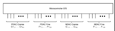
source/sink circuitry are shown in Figure 13. Shown are the coarse (CN,L) and
fine (FJ,N)
control signals for both the source circuitry (PDACs; designated with a "+")
and the sink
circuitry (NDACs; designated with a "-"). These control signals are ultimately
generated by
a microcontroller 570, which can be the microcontroller otherwise used to
implement the
logic functions in the IPG. Alternatively, the current source/sink circuitry
can be
implemented on an analog integrated circuit, which receives the control
signals from a digital
integrated circuit. Again, the specific details concerning the integration of
the current
source/sink circuitry with the logic can occur in any number of ways, as one
skilled in the art
will readily recognize.
[0066] Second, and unlike the prior art architectures discussed earlier,
circuitry is kept to a
minimum through reduction of the use of dedicated circuitry which otherwise
might be
guaranteed to go unused at particular points in time. In large part, this
benefit is the result of
14
CA 02665422 2009-04-03
WO 2008/048725 PCT/US2007/072238
the distributed nature of the coarse portion 402 of the circuitry across all
of the electrodes.
While the disclosed design does rely on the use of some dedicated
circuitry¨specifically, the
fine portion 403¨such circuitry is preferably kept to a minimum. In any event,
such
additional dedicated circuitry amounts to a good trade off when it is
recognized that this
reduces the number of necessary control signals.
[0067] Third, as compared to the prior art switch matrix approach of Figures 5
and 6, the new
architectures of Figures 8-12 comprise one less component in the output path,
which reduces
unwanted voltage drops in the output path and results in power savings. As can
be seen with
brief reference to Figures 9 and 10, which shows the circuitry in the coarse
portion 402, only
two components intervene between the power supply V+ and a given electrode:
the current
mirror output transistor(s) 413 and the selection switches 417 from the switch
banks 405.
Moreover, as concerns the fine portion 403, shown in Figure 11, again only two
components
intervene between the power supply V+ and a given electrode: the current
mirror output
transistors 422 and the selection switches 431. In addition to reducing the
series resistance in
the circuit by eliminating the series switch matrix, the selection switches
417 linearize the
current sources 410 by reducing the Vds voltage drop across the current
mirrors on electrodes
that require less compliance voltage than the difference of V+ to V-. If it
were not for the
switches 417, the entire excess compliance drop would be across the current
mirror 410 and
the current would tend to be a little higher than programmed on electrodes
requiring less
compliance voltage.
[0068] It should be understood that the direction in which current flows is a
relative concept,
and different conventions can be used to define whether currents flow to or
from various
sources. In this regard, arrows showing the directions of current flows in the
Figures,
references to current flowing to or form various circuit nodes, references to
currents being
sunk or sourced, etc., should all be understood as relative and not in any
limiting sense.
[0069] It should also be understood that reference to an electrode implantable
adjacent to
tissue to be stimulated includes electrodes on the implantable stimulator
device, or associated
electrode leads, or any other structure for stimulating tissue.
[0070] Moreover, it should be understood that an electrode implantable
adjacent to tissue to
be stimulated is to be understood without regard to any output capacitance,
such as coupling
capacitances CN included in the header connector 192 or elsewhere (see Fig.
7). This is so
because it should be understood that nodes on both sides of such a coupling
capacitor or other
output impedance are, in the context of this invention, not materially
different from an
CA 02665422 2009-04-03
WO 2008/048725 PCT/US2007/072238
architectural standpoint, such that either node would be considered as the
electrode node
implantable adjacent to tissue to be stimulated. The same would be true for
other
impedances, e.g., if an output resistor was used in addition to or in lieu of
a coupling
capacitor.
[0071] While the invention herein disclosed has been described by means of
specific
embodiments and applications thereof, numerous modifications and variations
could be made
thereto by those skilled in the art without departing from the literal and
equivalent scope of
the invention set forth in the claims.
16