Note: Descriptions are shown in the official language in which they were submitted.
CA 02666120 2009-04-08
WO 2008/057257 PCT/US2007/022657
ONE-TIME-PROGRAMMABLE LOGIC BIT WITH
MULTIPLE LOGIC ELEMENTS
FIELD OF THE INVENTION
This invention relates generally to integrated circuits, and more particularly
to
integrated circuits incorporating one-time-programmable logic memory.
BACKGROUND OF THE INVENTION
One-time-programmable ("OTP") memory elements are used in integrated
circuits ("IC") to provide non-volatile memory ("NVM"). Data in NVM are not
lost
when the IC is turned off. NVM allows an IC manufacturer to store lot number
and security data on the IC, for example, and is useful in many other
applications. Devices commonly known as fuses and anti-fuses are examples of
OTP memory elements.
Other types of devices, such as flash memory, are also used to provide NVM in
ICs; however, incorporating flash memory in a CMOS IC adds significant cost
because extra processing steps are typically required. Many types of fuses
exist, such as polysilicon fuses, metal fuses, contact fuses and via fuses,
that
are compatible with standard CMOS processing. However, high-density OTP
memory is typically less reliable and has a" lower programming yield than
similarly sized flash memory. It is therefore desirable to provide OTP memory
elements with better reliability and yield.
SUMMARY OF THE INVENTION
A memory cell with a logic bit has a first one-time-programmable ("OTP")
memory element providing a first OTP memory element output and a second
OTP memory element providing a second OTP memory element output. A logic
operator coupled to the first OTP memory element output and to the second
OTP memory element output and provides a memory output of the memory cell.
In a particular embodiment, the first OTP memory element is a different type
of
OTP memory than the second OTP memory element.
CA 02666120 2009-04-08
WO 2008/057257 PCT/US2007/022657
BRIEF DESCRIPTION OF THE DRAWINGS
FIG. 1 is a diagram of an IC with a memory element according to an embodiment
of the invention.
FIG. 2 is a circuit diagram of a memory cell according to an embodiment of the
invention.
FIG. 3 is a plan view of a memory element with two different types of OTP
devices according to an embodiment.
FIG. 4 shows programming conditions for an OTP-type logic bit according to an
embodiment.
FIG. 5 is a plan view of an FPGA according to an embodiment.
FIG. 6 is a flow chart of a method of operating a memory cell according to an
embodiment of the invention.
DETAILED DESCRIPTION OF THE DRAWINGS
FIG. 1 is a diagram of an IC 100 with a logic bit 102 according to an
embodiment
of the invention. The logic bit 102 is part of a memory cell 104 that provides
a
datum at an output 106. The datum is a binary "1" or "0" logic value, for
example, and is typically read by other circuitry of the IC (not shown).
Additional
parts of the memory cell 104, such as sense amplifiers and latches (see FIG.
2),
are familiar to those of skill in the art of OTP memory, and are omitted for
simplicity and clarity of illustration.
The logic bit 102 has two OTP memory elements 108, 110, such as two fuses.
In a particular embodiment, the first OTP memory element 108 is a first type
of
fuse and the second OTP memory element 110 is a second type of fuse. For
example, the first OTP memory element is a poly-silicon-based fuse ("poly-
fuse")
and the second OTP memory element is a thin-film metal fuse, or the first OTP
memory element is a narrow poly-fuse and the second OTP memory element is
a wide poly-fuse. The term "type" of fuse is used to denote that the first
type of
OTP memory element is intentionally different from the second type of element.
In an alternative embodiment, the first OTP memory element is a first type of
fuse, and the second OTP memory element is the same type of fuse as the first.
Although providing two OTP memory elements in a single logic bit consumes
more area of the IC chip, the improved yield and reliability of the resultant
NVM
make logic.cells with redundant OTP memory elements desirable.
2
CA 02666120 2009-04-08
WO 2008/057257 PCT/US2007/022657
In general, different types of fuses program differently during a programming
process. In a given programming process-(e.g., applying a 10 mA current to the
fuse at a programming voltage of about 3.3 V for about 500 micro-seconds to
about 1200 micro-seconds), fuse elements are converted from a relatively low
resistance condition (typically about 100 Ohms to about 300 Ohms) to a
relatively high resistance condition (typically about 10 kOhms to greater than
about 100 MOhms). It is desirable that the final (programmed) resistance be
sufficiently different from the initial (unprogrammed) resistance to easily
distinguish between the programmed and unprogrammed conditions, which
represent different logic states when the fuses are used as memory elements.
Fuse elements in a memory array will have a distribution of both unprogrammed
resistance and programmed resistance that arises from physical variations in
the
manufacturing process and in the programming process. That is, fuse links will
have slight variations in width, thickness, and conductivity that will affect
the
initial and final resistance, as well as programmability. Even heat
dissipation
from a fuse link can add a variation to programmed resistance. A programming
process is typically optimized for a type of fuse, but process variations can
affect
the programming results (final resistivity distribution (sense current
distribution)
and yield). For example, a weakly programmed fuse (e.g., a fuse having a
programmed resistance of about 1 kOhm) may pass the program verification, but
become more conductive over time, causing a reliability failure.
Providing two OTP memory elements 108, 110 in a single logic bit 102 improves
yield (particularly programmed yield) and reliability of OTP-based on-chip
memory. While advantages are obtained using the same type of OTP memory
elements in a logic bit, using two different types of OTP memory elements in a
single logic bit is particularly desirable because such an arrangement
provides
wider margins for both manufacturing and programming process.
The outputs 109 and 111 of the OTP memory elements 108 and 110,
respectively, are provided to logic operator ("gate") 112, which in this
example is
an OR gate. The logic operator 112 provides the logic output 106 of the memory
cell 104. For example, if either of the OTP memory elements 108 and 110 is
programmed to a logic "1" state, then the memory cell (output 106) will
indicate a
logic value of "1" for the memory cell 104. In many cases, the second OTP
memory element is redundant in that, if the first OTP memory element is
3
CA 02666120 2009-04-08
WO 2008/057257 PCT/US2007/022657
successfully programmed, the second OTP memory element does not affect the
value of the logic bit. However, if the first OTP memory element fails in
either
programming or sense (READ), a properly operating second OTP memory
element ensures that the logic bit provides the correct value. In a typical
application, most or all of the logic bits in an OTP-based NVM memory array
include both first and second (i.e., redundant) OTP memory elements. In an
exemplary operation, both OTP memory elements 108, 110 are programmed.
In one embodiment, both are programmed using the same programming
process. This approach is particularly desirable in embodiments where the
first
OTP memory element is of a first type, and the second OTP memory element is
of a second type, where the types of OTP memory elements have been selected
so as to provide high programming yield of at least one of the first type or
second
type of OTP memory elements during the programming process. Such
techniques can be used, for example, when the programming windows (see FIG.
4) for both types of devices overlap; however, this is not essential. In
another
embodiment, one type of OTP memory element is programmed at the same
voltage and current as the second type of OTP memory element, but the
programming signal is applied to the different types of OTP memory elements
for
different lengths of time.
For example, if normal manufacturing variations produce a programmed
resistivity for the first type of OTP memory elements that is out-of-
specification
for a number of logic bits, selecting a second type of OTP memory element that
is likely to be successfully programmed when the first type is not
successfully
programmed enhances programming yield of the logic bits. In a particular
example, the first OTP memory element is a first type of poly-fuse having a
relatively narrow and short neck (fusible link), and the second type is a poly-
fuse
having a relatively wide and long neck. In a particular embodiment, the first
type
of fuse has a neck that is at least 30% more narrow than the neck on the
second
type of fuse.
The wide fuse could be optimally programmed at one programming condition
(e.g., a first programming duration), while the narrow fuse could be optimally
programmed at a different programming condition (e.g., a second programming
duration). The combination of the two types of OTP devices provides one
logical
bit. Even though the programming conditions will naturally program some fuses
4
CA 02666120 2009-04-08
WO 2008/057257 PCT/US2007/022657
differently than others, providing redundant OTP memory elements in a single
logic bit enhances program yield and reliability of the logic bit.
In an alternative embodiment, the first OTP memory element 108 is programmed
using a first programming process, and the second OTP memory element 110 is
programmed using a second programming process (technique or sequence).
The resulting OTP-based memory array has a higher programming yield and
improved reliability and sensing margin, compared to a conventional OTP-
memory array having only a single OTP memory element for each logic bit.
FIG. 2 is a circuit diagram of a memory cell 200 according to an embodiment of
the invention. Memory cells having a single OTP memory element for each logic
bit are well-known in the art; therefore, only a brief description of the
memory cell
and its operation is provided. The memory cell 200 has two OTP memory
elements 108 and 110, such as fuses or anti-fuses. In a particular embodiment,
the first OTP memory element 108 is of the first type, and the second OTP
memory element 110 is of the second type. Program enable transistors 202 and
204 provide current paths for programming current supplied at associated
programming pads 206 and 208, respectively. Programming voltage Vfs is
applied to the programming pads 206 and 208 and the programming transistors
202 and 204 are turned on by applying a programming signal Vpp to their gate
terminals for a selected period of time Tpgm. The programming transistors 202,
204 and Vpp can be selected to provide the desired programming current through
the fuse element during programming.
After programming the OTP memory elements 108 and 110, the logic state
(resistivity) of the OTP memory elements is sensed using sense enable
transistors 210, 212, 214, 216, as is well known in the art. The sensed logic
state for each OTP memory element is captured by associated latches 218 and
220 and the outputs (logic states) 109 and 111 of the OTP memory elements
108 and 110 are provided to the OR gate 112. If one or both of the OTP
memory elements indicate a logic "1" state, then the output 106 of the memory
cell 200 is "1 ". Of course, those of skill in the art will appreciate that
the logic
values and functions chosen in this example are merely exemplary, and other
values and functions are alternatively used. For example, both OTP memory
elements are alternatively anti-fuse devices, and the logic operator is a NOR
gate, or one of the OTP memory elements is a fuse, and the other is an anti-
fuse
5
CA 02666120 2009-04-08
WO 2008/057257 PCT/US2007/022657
with an inverter between it and an OR operator, or the OR operator is replaced
with a NAND operator.
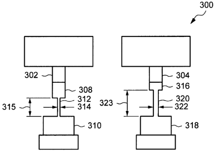
FIG. 3 is a plan view of a logic bit 300 with two different types of OTP
devices
302, 304 according to an embodiment. The first OTP device 302 is a narrow
poly-fuse having an anode 308, a cathode 310, and a fuse neck 312 having a
width 314 and a length 315. The second OTP device 304 is a wide poly-fuse
having a second anode 316, a second cathode 318, and a second fuse neck 320
having a second width 322, and a second length 323. The terms "narrow" and
"wide" mean that the second fuse neck 320 is designed to be selectively wider
than the first fuse neck 312 (i.e., width 322 is greater than width 314).
In a particular embodiment, the first neck 312 is about 80 nm wide and about
800 nm long, and the second neck 320 is about 120 nm wide and about 1.2
micrometers long to keep the same resistance-square ("R-square") value, which
provides essentially the same unprogrammed resistance for each type of fuse,
so that the same programming current can be used. Fuses are typically
programmed one-by-one. Programming current is provided by a programming
transistor, and is switched to the fuse, as is known in the art of OTP fuse
programming. Providing two different types of OTP devices having essentially
the same unprogrammed resistance draws similar current from the programming
transistor when each of the devices is being programmed. This allows use of a
common, stable, current source when programming both types of fuses. It is
desirable to accurately control the current used for programming fuses. Other
programming parameters, such as the duration of the programming current, may
be separately optimized for each type of fuse. Duration of the current is
relatively easy to accurately control and change.
The first and second poly-fuses 302, 304 are fabricated in an IC having the
logic
bit using a standard CMOS fabrication process. That is, no materials or
process
steps are required that are not already part of the CMOS IC fabrication
technique. This is desirable because it provides OTP-based NVM on the IC
without adding additional processes to the IC fabrication sequence.
In one example, the poly fuses are similar to gate structures in a CMOS IC.
The
fuse necks are fabricated on what is conventionally referred to as the gate
dielectric layer, which in a particular example is an STI oxide layer. The
fuse
neck has a layer of p+-doped poly-silicon formed on the gate dielectric layer,
and
6
CA 02666120 2009-04-08
WO 2008/057257 PCT/US2007/022657
a layer of silicide, such as nickel silicide, is formed on the poly-silicon. A
layer of
silicon nitride is formed on the silicide. During programming, the conductive
silicide element electro-migrates with the electron flow from cathode to
anode,
and the silicide of the element will accumulate on the anode side. Therefore,
little
or no silicide remains in the locality of the fuse neck and the fuse neck now
has a
high resistance, which will cause Joule heating. The high temperature from
this
Joule heating depletes dopant species (e.g., boron ions) inside the poly fuse
neck to the anode and cathode sides of the fuse. Subsequently, the fuse self-
quenches and cools down to become programmed to a very high resistance.
FIG. 4 shows programming conditions for an OTP-type logic bit according to an
embodiment. A first programming process window 400 shows the programming
current and voltage conditions that provide reliable programming of a first
type
(Type 1) of OTP memory element, such as a poly-fuse. A second programming
process window 402 shows the programming current and voltage conditions that
provide reliable programming of a second type (Type 2) of OTP memory
element, such as a second type of poly-fuse. The first and second
programming process windows overlap to form an overlap process window 404
(defined by the dashed lines). A programming condition, such as that defined
by
the current and voltage at 406, should reliably program both Type 1 and Type 2
OTP memory elements. In an alternative embodiment, the programming process
windows of the selected of OTP memory elements do not overlap. Note that in
alternative embodiments, for even greater reliability, more than two OTP
memory
elements may be used.
If the program voltage drifts high, for example to point 408, the Type 2 OTP
memory element would still be reliably programmed, even though the Type 1
OTP memory element might not be reliably programmed. If the program voltage
drifts low, for example to point 410, The Type 1 OTP memory element would
still
be reliably programmed, even though the Type 2 OTP memory element might
not be reliably programmed. The programming process window for a logic bit
having both Type 1 and Type 2 OTP memory elements is defined by the solid
outer perimeter 412 of the first and second programming process windows 400,
402. A programming condition occurring anywhere within this programming
process window 412 would be expected to program at least one of the Type 1 or
Type 2 OTP memory elements, and in some instances, reliably program both.
7
CA 02666120 2009-04-08
WO 2008/057257 PCT/US2007/022657
Thus, a logic bit according to embodiments is reliably programmed over a
greater range of programming conditions than a conventional logic bit having
only one type of OTP memory element.
Other programming parameters could be used to similarly illustrate that logic
bits
having different types of OTP memory elements provide improved programming
yield over a wider range of programming and OTP memory element fabrication
process variations.
Test chips were fabricated with two different types of poly-fuses using a 65
nm
CMOS fabrication process. A first programming process was used to program
the first type of poly-fuse, and a second programming process was used to
program the second type of poly-fuse. The two types of programming processes
were optimized for each type of fuse. The-test chips were evaluated for
programming quality (programmed resistance). The data obtained from these
test chips showed better programming reliability and programming yield of
logic
bits.
FIG. 5 is a plan view of an integrated circuit 500 according to an embodiment
of
the invention. The integrated circuit is an FPGA (field programmable gate
array)
that includes CMOS portions in several of the functional blocks, such as in
RAM
and logic, and is fabricated using a CMOS fabrication process. Logic bits
having
multiple OTP memory elements according to one or more embodiments of the
invention are incorporated in any of several functional blocks of the IC, such
as a
memory block, logic block, I/O block, clock circuit, transceiver, or other
functional
block; within many functional blocks; or within a physical section or segment
of
the FPGA 500. Logic bits having redundant (dual) OTP memory elements (e.g.,
fuses) according to embodiments of the invention are particularly desirable in
FPGAs because they provide reliable, secure on-chip NVM for a variety of
purposes. For example, they may be used for component identification, or to
avoid having to download the data stored in the on-chip NVM from an external
source to the IC, which can be time consuming and can be intercepted. In
another example application, on-chip OTP NVM according to an embodiment
may be used to de-crypt (for example by storing one or more decryption keys) a
bitstream transferred from an external source to the FPGA, such as data or a
configuration file. For instance, an un-encrypted configuration bitstream
could
be intercepted during transmission. Design security in FPGAs may be enabled
8
CA 02666120 2009-04-08
WO 2008/057257 PCT/US2007/022657
by encrypting the configuration bitstream, and using the OTP-based NVM on the
FPGA to decrypt the configuration bitstream. Storing an on-chip
encryption/decryption key in OTP NMV requires relatively little memory, and
thus
consumes little space on the IC. Although dual-OTP memory element memory
arrays consume more chip area than single-OTP memory element memory
arrays, this penalty is minor, and is worth the enhanced manufacturability and
reliability. Another example use of dual-OTP memory element memory is to
store a small number of bits (typically 100 bits or less) to provide a digital
tuning
function, such as tuning an on-chip amplifier or oscillator. Embodiments of
the
invention provide easily manufactured, reliable on-chip NVM, and incur minimal
size penalties in low-density storage applications. The NVM retains its
information when power is off, eliminating the need for a battery backup or
other
continuous power supply to the FPGA.
The FPGA architecture includes a large number of different programmable tiles
including multi-gigabit transceivers (MGTs 501), configurable logic blocks
(CLBs
502), random access memory blocks (BRAMs 503), input/output blocks (IOBs
504), configuration and clocking logic (CONFIG/CLOCKS 505), digital signal
processing blocks (DSPs 506), specialized input/output blocks (I/O 507) (e.g.,
configuration ports and clock ports), and other programmable logic 508 such as
digital clock managers, analog-to-digital converters, system monitoring logic,
and
so forth. Some FPGAs also include dedicated processor blocks (PROC 510).
In some FPGAs, each programmable tile includes a programmable interconnect
element (INT 511) having standardized connections to and from a corresponding
interconnect element in each adjacent tile. Therefore, the programmable
interconnect elements taken together implement the programmable interconnect
structure for the illustrated FPGA. The programmable interconnect element (INT
511) also includes the connections to and from the programmable logic element
within the same tile, as shown by the examples included at the top of FIG 5.
For example, a CLB 502 can include a configurable logic element (CLE 512) that
can be programmed to implement user logic plus a single programmable
interconnect element (INT 511). A BRAM 503 can include a BRAM logic
element (BRL 513) in addition to one or more programmable interconnect
elements. Typically, the number of interconnect elements included in a tile
depends on the height of the tile. In the pictured embodiment, a BRAM tile has
9
CA 02666120 2009-04-08
WO 2008/057257 PCT/US2007/022657
the same height as four CLBs, but other numbers (e.g., five) can also be used.
A DSP tile 506 can include a DSP logic element (DSPL 514) in addition to an
appropriate number of programmable interconnect elements. An IOB 504 can
include, for example, two instances of an input/output logic element (IOL 515)
in
addition to one instance of the programmable interconnect element (INT 511).
As will be clear to those of skill in the art, the actual I/O pads connected,
for
example, to the I/O logic element 515 are manufactured using metal layered
above the various illustrated logic blocks, and typically are not confined to
the
area of the input/output logic element 515. In the pictured embodiment, a
columnar area near the center of the die (shown shaded in FIG. 5) is used for
configuration, clock, and other control logic.
Some FPGAs utilizing the architecture illustrated in FIG. 5 include additional
logic blocks that disrupt the regular columnar structure making up a large
part of
the FPGA. The additional logic blocks can be programmable blocks and/or
dedicated logic. For example, the processor block PROC 510 shown in FIG. 5
spans several columns of CLBs and BRAMs.
Note that FIG. 5 is intended to illustrate only an exemplary FPGA
architecture.
The numbers of logic blocks in a column, the relative widths of the columns,
the
number and order of columns, the types of logic blocks included in the
columns,
the relative sizes of the logic blocks, and the interconnect/logic
implementations
included at the top of FIG. 5 are purely exemplary. For example, in an actual
FPGA more than one adjacent column of CLBs is typically included wherever the
CLBs appear, to facilitate the efficient implementation of user logic.
FIG. 6 is a flow chart of a method 600 of operating a memory cell according to
an embodiment of the invention. A first programming condition is applied to a
first one-time-programmable ("OTP") memory element in a logic bit (step 602).
A
second programming condition is applied to a second OTP memory element in
the logic bit (step 604).
In a particular embodiment, the first programming condition (e.g., programming
voltage, programming current, and current pulse duration) is the same as the
second programming condition. In an alternative embodiment, the first
programming condition is optimized for programming the first OTP memory
element, and the second programming condition is optimized for programming
the second OTP memory element. In a particular embodiment, the first.
CA 02666120 2009-04-08
WO 2008/057257 PCT/US2007/022657
programming condition has a first programming process window, and the second
programming condition has a second programming process window. The first
programming process window at least partially overlaps the second
programming process window to form an overlap programming process window
for the logic bit.
A first memory element output from the first OTP memory element and a second
memory element output from the second OTP memory element in the logic bit
are coupled to a logic operator of the memory cell (step 606), and the logic
operator is operated (step 608) so as to provide a logic output from the
memory
cell according to the first memory element output, the second memory element
output, and the logic operator. In a particular embodiment, the first and
second
OTP memory elements are fuses, and the logic operator is an OR gate. In a
particular embodiment, the logic output from the memory cell is part of a
decryption key. In a further embodiment, the logic output from the memory cell
is used to decrypt a configuration bitstream of a field programmable gate
array.
In an alternative embodiment, the logic output from the memory cell provides
component identification of an FPGA.
While the present invention has been described in connection with specific
embodiments, variations of these embodiments will be obvious to those of
ordinary skill in the art. Therefore, the spirit and scope of the appended
claims
should not be limited to the foregoing description.
11