Language selection

Search

Patent 2666483 Summary

Third-party information liability

Some of the information on this Web page has been provided by external sources. The Government of Canada is not responsible for the accuracy, reliability or currency of the information supplied by external sources. Users wishing to rely upon this information should consult directly with the source of the information. Content provided by external sources is not subject to official languages, privacy and accessibility requirements.

Claims and Abstract availability

Any discrepancies in the text and image of the Claims and Abstract are due to differing posting times. Text of the Claims and Abstract are posted:

  • At the time the application is open to public inspection;
  • At the time of issue of the patent (grant).
(12) Patent: (11) CA 2666483
(54) English Title: RF TERMINATING RESISTOR OF FLANGED CONSTRUCTION
(54) French Title: RESISTANCE DE CLOTURE HF A STRUCTURE EN BRIDES
Status: Deemed Expired
Bibliographic Data
(51) International Patent Classification (IPC):
  • H01C 07/00 (2006.01)
  • H01C 01/14 (2006.01)
  • H01P 01/26 (2006.01)
(72) Inventors :
  • WEISS, FRANK (Germany)
(73) Owners :
  • ROSENBERGER HOCHFREQUENZTECHNIK GMBH & CO. KG
(71) Applicants :
  • ROSENBERGER HOCHFREQUENZTECHNIK GMBH & CO. KG (Germany)
(74) Agent: SMART & BIGGAR LP
(74) Associate agent:
(45) Issued: 2016-01-05
(86) PCT Filing Date: 2007-11-07
(87) Open to Public Inspection: 2008-06-19
Examination requested: 2012-10-16
Availability of licence: N/A
Dedicated to the Public: N/A
(25) Language of filing: English

Patent Cooperation Treaty (PCT): Yes
(86) PCT Filing Number: PCT/EP2007/009645
(87) International Publication Number: EP2007009645
(85) National Entry: 2009-04-15

(30) Application Priority Data:
Application No. Country/Territory Date
20 2006 018 768.5 (Germany) 2006-12-12

Abstracts

English Abstract

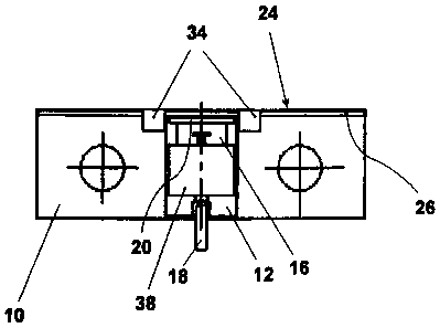
In the case of an RF terminating resistor with a flange body (10) and a planar layer structure (16, 18, 20) which is arranged on it and, on an upper face (14) of a substrate (12), has a resistance layer (16) for conversion of RF energy to heat, an input conductor track (18) for supplying RF energy, and an earth connection conductor track (20) for electrical connection to an earth contact on the flange body (12), with the input conductor track (18) being electrically connected to a first end of the resistance layer (16), with the earth connection conductor track (20) being electrically connected to a second end of the resistance layer (16) opposite the first end, and with the substrate (12) having a contact face (22), facing away from the layer structure (16, 18, 20), which rests on the flange body, the arrangement is designed such that, on a first edge (24) which faces the earth connection conductor track (20) on the substrate (12), the flange body (10) is bent around in a direction parallel to this edge (24) over at least one predetermined section, and a predetermined section is bent around in a direction at right angles to this edge (24), such that the bent-around section (26) of the flange body (10) extends in a space between a first plane, defined by the contact face (22) of the substrate (12), and a second plane, defined by the upper face (14) of the substrate (12), with the substrate (12) abutting on the bent-around section (26) of the flange body (10) with a face (28) which connects the contact face (22) of the substrate (12) to the upper face (14) of the substrate (12) and faces the earth connection conductor track (20) on the upper face (14) of the substrate (12).


French Abstract

L'invention concerne une résistance de clôture HF qui présente un corps de bride (10) sur lequel est disposée une structure stratifiée plane (16, 18, 20) qui présente sur le côté supérieur (14) d'un substrat (12) une couche résistive (16) qui convertit l'énergie HF en chaleur, une piste (18) de guide d'entrée qui amène l'énergie HF et une piste (20) de guide de raccordement à la masse qui assure la liaison électrique avec un contact de masse prévu sur le corps de bride (10). La piste (18) de guide d'entrée est reliée électriquement à une première extrémité de la couche résistive (16), la piste (20) de guide de raccordement à la masse est reliée électriquement à une deuxième extrémité de la couche résistive (16) opposée à la première extrémité et le substrat (12) repose sur le corps de bride (10) par un côté de pose (22) non tourné vers la structure stratifiée (16, 18, 20). L'agencement est formé en ce que sur un premier côté (24) tourné vers la piste (20) de guide de raccordement à la masse situé sur le substrat (12), le corps de bride (10) est rabattu sur au moins une partie prédéterminée dans une direction parallèle à ce bord (24) ainsi que sur une partie prédéterminée dans la direction perpendiculaire à ce bord (24), de telle sorte que la partie rabattue (26) du corps de bride (10) s'étend dans un espace situé entre un premier plan défini par le côté de pose (22) du substrat (12) et un deuxième plan défini par le côté supérieur (14) du substrat (12). Un côté (28) du substrat (12), qui relie le côté de pose (22) du substrat (12) au côté supérieur (14) du substrat (12) et vers lequel la piste (20) de guide de raccordement de masse située sur le côté supérieur (14) du substrat (12) est tournée, vient buter contre la partie rabattue (26) du corps de bride (10).

Claims

Note: Claims are shown in the official language in which they were submitted.


9
Claims
1. RF terminating resistor with a flange body and a planar
layered structure arranged thereon, which comprises, on an upper
face of a substrate, a resistor layer for converting RF energy
into heat, an input conductor track for supplying RF energy and
an earth connection conductor track for electrical connection to
an earth contact on the flange body, wherein the input conductor
track is electrically connected to a first end of the resistor
layer, the earth connection conductor track is electrically
connected to a second end of the resistor layer opposing the
first end, and the substrate lies on the flange body with a
contact face which faces away from the layered structure,
characterised in that, at a first edge which faces toward the
earth connection conductor track on the substrate, over at least
one predetermined section in a direction parallel to said edge
and a predetermined section in a direction perpendicular to said
edge, the flange body is bent over such that the bent-over
section of the flange body extends into a space between a first
plane defined by the contact face of the substrate and a second
plane defined by the upper face of the substrate, wherein, with
one side which connects the contact face of the substrate to the
upper face of the substrate and towards which the earth
connection conductor track on the upper face of the substrate
faces, the substrate abuts the bent-over section of the flange
body, wherein the bent-over section of the flange body has at
least two noses, the separation of which in the direction
parallel to the first edge of the flange body corresponds to the
width of the substrate, and which extend into a space between
the first plane and the second plane.

10
2. RF terminating resistor according to claim 1, wherein
the bent-over section of the flange body rises from the first
plane at least into the second plane or therebeyond, such that
at least one section of the bent-over section of the flange body
extends in the second plane adjacent to the earth connection
conductor track.
3. RF terminating resistor according to any one of claims 1
or 2, wherein the bent-over section of the flange body has a
length in a direction parallel to the first edge which
corresponds to at least a width of the substrate.
4. RF terminating resistor according to any one of claims
1, 2 or 3, wherein the bent-over section encloses an angle of
90° with the first plane on a side facing toward the substrate.
5. RF terminating resistor according to any one of claims
1, 2, 3 or 4, wherein the bent-over section encloses an angle
with the first plane on a side facing towards the substrate of
less than 90°, in particular 86° to 80°.
6. RF terminating resistor according to any one of claims 1
to 4, wherein an angle between the bent-over section of the
flange body and a perpendicular to the upper face of the
substrate has a value in the range of 4° to 10°.

Description

Note: Descriptions are shown in the official language in which they were submitted.


CA 02666483 2009-04-15
WO 2008/071271 PCT/EP2007/009645
RF Terminating Resistor of Flanged Construction
Description
The present invention relates.to an RF terminating
resistor with a flange body and a planar layered structure
arranged thereon, which comprises, on an upper face of a
substrate, a resistor layer for converting RF energy into
heat, an input conductor track for supplying RF energy and
an earth connection conductor track for electrical
connection to an earth contact on the flange body, wherein
the input conductor track is electrically connected to a
first end of the resistor layer, the earth connection
conductor track is electrically connected to a second end
of the resistor layer opposing the first end and the
substrate lies on the flange body with a contact face which
faces away from the layered structure, according to the
preamble of claim 1.
Broadband RF terminating resistors of flanged
construction serve to conduct away large power losses. It
is known to mount a resistor structure on a substrate and
to arrange said substrate on a flange body which represents
an earth contact. In order to create an electrical
connection from the resistor structure to the earth contact
of the flange body, it is necessary to build up an edge
peripheral contact round the substrate or a substrate
through contact to the earth connection. However, both are
complex and costly.
It is an object of the invention to improve an RF
terminating resistor of the aforementioned type with regard
to its design and production and also not to worsen the

p . i
CA 02666483 2009-04-15
WO 2008/071271 2 PCT/EP2007/009645
electrical properties of the RF terminating resistor, but
rather to improve them.
This aim is achieved according to the invention with
an RF terminating resistor of the aforementioned type and
having the characterising features of claim 1. Advantageous
embodiments of the invention are described in the other
claims.
In an RF terminating resistor of the aforementioned
type, it is provided according to the invention that, at a
first edge which faces toward the earth connection
conductor track on the substrate, over at least one
predetermined section in a direction parallel to said edge
and a predetermined section in a direction perpendicular to
said edge, the flange body is bent over such that the bent-
over section of the flange body extends into a space
between a first plane defined by the contact face of the
substrate and a second plane defined by the upper face of
the substrate, wherein, with one side which connects the
contact face of the substrate to the upper face of the
substrate and towards which the earth connection conductor
track on the upper face of the substrate faces, the
substrate abuts the bent-over section of the flange body.
This has the advantage that, in order to produce the
electrical contact between the earth connection conductor
track and the earth contact on the flange body, a costly
edge peripheral contact round one side of the substrate is
not necessary, but rather this electrical contact is
arranged in the second plane of the upper side of the
substrate on which the earth connection conductor track is
arranged on the substrate, can be easily produced by
electrically connecting the earth connection conductor
track to the bent-over section of the flange body.

CA 02666483 2009-04-15
WO 2008/071271 3 PCT/EP2007/009645
An electrical contact between the earth connection
contract track and the bent-over section of the flange body
can be particularly easily achieved in that the bent-over
section of the flange body rises from the first plane at
least into the second plane or therebeyond, such that at
least one section of the bent-over section of the flange
body extends in the second plane adjacent to the earth
connection conductor track.
Suitably, the bent-over section of the flange body has
a length in a direction parallel to the first edge which
corresponds to at least a width of the substrate.
In that the bent-over section of the flange body has
at least two noses, the separation of which in the
direction parallel to the first edge of the flange body
corresponds to the width of the substrate, and which,
starting from the elevation, extend into a space between
the first plane and the second plane, a stop is provided on
both sides for the substrate, fixing a position of the
substrate on the flange body even before the fastening of
the substrate onto the flange body.
Suitably,.the bent-over section encloses an angle of
90 with the first plane on a side facing toward the
substrate.
In order to ensure that the bent-over section touches
the substrate, the bent-over section encloses an angle with
the first plane on a side facing towards the substrate of
less than 90 , in particular 86 to 80 .
The invention will now be described in greater detail
by reference to the drawings, in which:
Fig. 1 shows a preferred embodiment of an RF
terminating resistor according to the invention in a plan
view,

CA 02666483 2009-04-15
WO 2008/071271 4 PCT/EP2007/009645
Fig. 2 shows the RF terminating resistor according to
Fig. 1 in a side view,
Fig. 3 shows a flange body for an RF terminating
resistor according to the invention in a plan view,
Fig. 4 shows the flange body of Fig. 3 in a side view,
Fig. 5 shows the detail Z of Fig. 4, and
Fig. 6 shows the flange body of Fig. 3 in an unrolled
representation.
The preferred embodiment of an RF terminating resistor
of flange construction according to the invention shown in
Figs. 1 and 2 comprises a flange body 10 on which a
substrate 12 is arranged. Arranged on an upper face 14 of
the substrate 12 is a layered structure which comprises a
resistor layer 16 for converting RF energy into heat, an
i5 input conductor track 18 for supplying RF energy and an
earth connection conductor track 20 for electrical
connection to an earth contact on the flange body-10: The
input conductor track 18 is electrically connected to a
first end of the resistor layer 16. The earth connection
conductor track 20 is electrically connected to a second
end of the resistor layer 16 opposing the first end. The
substrate 12 lies with a contact face 22 which faces away
from the layered structure 16, 18, 20 on the flange body
10.
The flange body 10 has an edge 24 wherein the
substrate 12 is arranged with the layered structure 16, 18,
20 mounted thereon on the flange body 10 such that the
earth connection conductor track 20 faces towards said edge
24.
The contact face 22 of the substrate 12 defines a
first plane and the upper face 14 of the substrate 12
defines a second plane.

CA 02666483 2009-04-15
WO 2008/071271 5 PCT/EP2007/009645
As shown also by Figs. 3 to 6, over a predetermined
section in a direction parallel to the edge 24 and over a
predetermined section in a direction perpendicular to the
edge 24, said edge 24 is bent over. In the exemplary
embodiment shown in the figures, the predetermined section
extends parallel to the edge 24 over the whole length of
the edge 24. This predetermined section parallel to the
edge 24 can alternatively extend over just part of the
length of the edge 24, for example, over a length
corresponding to the width of the substrate 12 in a
direction parallel to the edge 24.
The bent-over section 26 of the flange body 10 is
configured and bent over in such a way that the bent-over
section 26 extends at least into the space between the
first and second planes. In the exemplary embodiment shown,
the bent-over section 26 extends completely through the
space between the first and second planes as far as the
second plane and further beyond the second plane. However,
it is also possible for the bent-over section 26 to extend
exactly as far as the second plane or to end within the
space between the first and second planes.
The substrate 12 makes contact with a short face 28,
which connects the upper face 14 of the substrate 12 to the
contact face 22 of the substrate 12, on the bent-over
section 26 of the flange body 10. The short face 28 is the
face of the substrate 12 which faces towards the earth
connection conductor track 20 on the upper face 14 of the
substrate 12. In order to ensure this abutting of the short
face 28 against the bent-over section 26 of the flange body
10 in any event, it is particularly advantageous if the
bent-over section 26 of the flange body 10 is bent over by
more than 90 relative to the flange body 10. This produces
an angle between the bent-over section 26 of the flange

CA 02666483 2009-04-15
WO 2008/071271 6 PCT/EP2007/009645
body 10 and the upper face of the substrate 12 or between
the bent-over section 26 and the plane defined by said
upper face on a side facing towards the substrate 12 of
less than 90 , for example 86 to 80 . Expressed otherwise,
an angle 30 between the bent-over section 26 of the flange
body 10 and a perpendicular 32 to the upper face 14 of the
substrate 12 has a value in the range of 4 to 10 .
Also arranged on the bent-over section 26 of the
flange body 10 are two noses 34 which extend beyond the end
of the bent-over section 26 and.are bent over relative to
the bent-over section 26 by a further angle 36 of, for
example 45 . These noses 34 therefore extend back into the
space between the first and second planes. The spacing
between these noses 34 in a direction parallel to the edge
24 of the flange body 10 corresponds approximately to the
width of the substrate 12 in the direction parallel to the
edge 24. By this means, the position of the substrate 12 on
the flange body 10 and relative to the bent-over section 26
is fixed by positioning between the noses 34 and simplifies
mounting of the substrate 12 on the flange body 10.
The bent-over section 26 of the flange body 10 forms
the earth contact for the earth connection conductor track
20. In that the bent-over section 26 extends into the space
between the first and second planes, electrical contact can
easily be created between the earth connection conductor
track 20 and the bent-over section 26 without complete edge
peripheral contact round the short face 28 of the substrate
12. In the exemplary embodiment shown, the bent-over
section 26 extends above the second plane or the upper face
14 of the substrate 12, so that the electrical contact
between the earth connection conductor track 20 and the
bent-over section 26 of the flange body 10 can be created
directly in one plane, specifically the second plane of the

CA 02666483 2009-04-15
WO 2008/071271 7 PCT/EP2007/009645
upper face 14 of the substrate 12. This simplifies the
creation of the electrical contact and, simultaneously,
improves the electrical properties of the RF terminating
resistor, since the path of the electrical contact is as
short as possible and no longer leads completely round an
edge of the substrate 12.
A covering 38 partially covers the layered structure
16, 18, 20. This covering is made, for example, from the
same material as the substrate 12. The covering 38
therefore has the same dielectric constant as the material
of the substrate 12. This also positively influences the
electrical properties of the RF terminating resistor, since
due to the dielectric (12, 38), that is, the substrate 12
on one side and the covering 38 on the other side, which is
identical on both sides, the electric field is guided close
to the layered structure 16, 18, 20.
Thanks to the improved design of the RF terminating
resistor according to the invention, inexpensive substrates
12, that is substrates without an edge peripheral contact,
can be used. The overall design of the flanged load ensures
the transfer of large power losses whilst maintaining the
best possible broadband RF properties.
The flange body or the flange sheet 10 with the bent-
over section 26 is made entirely from one piece, for
example, a press-bent part. The bent-over section 26 serves
for the earth connection of the resistor structure 14 to
the flange sheet 10. The overall construction including the
substrate structure 12, 16, 18, 20 is intended for a
broadband application with very good RF properties.
In order to produce an electrical connection between
the earth connection conductor track 20 on the substrate 12
and the bent-over section 26 of the flange body 10, so that
the earth contact for the RF terminating resistor is made,

CA 02666483 2009-04-15
WO 2008/071271 8 PCT/EP2007/009645
for example, a solder joint is made from the earth
connection conductor track 20 to the bent-over section 26.
In that the bent-over section 26 extends in particularly
advantageous manner as far as or beyond the upper face 14
of the substrate 12 (second plane), said solder joint can
be made easily, quickly and inexpensively in the second
plane of the upper face 14 of the substrate.12.

Representative Drawing
A single figure which represents the drawing illustrating the invention.
Administrative Status

2024-08-01:As part of the Next Generation Patents (NGP) transition, the Canadian Patents Database (CPD) now contains a more detailed Event History, which replicates the Event Log of our new back-office solution.

Please note that "Inactive:" events refers to events no longer in use in our new back-office solution.

For a clearer understanding of the status of the application/patent presented on this page, the site Disclaimer , as well as the definitions for Patent , Event History , Maintenance Fee  and Payment History  should be consulted.

Event History

Description Date
Letter Sent 2024-05-07
Letter Sent 2023-11-07
Common Representative Appointed 2019-10-30
Change of Address or Method of Correspondence Request Received 2018-01-12
Grant by Issuance 2016-01-05
Inactive: Cover page published 2016-01-04
Pre-grant 2015-08-17
Inactive: Final fee received 2015-08-17
Notice of Allowance is Issued 2015-07-03
Letter Sent 2015-07-03
Notice of Allowance is Issued 2015-07-03
Inactive: QS passed 2015-05-19
Inactive: Approved for allowance (AFA) 2015-05-19
Amendment Received - Voluntary Amendment 2015-01-07
Inactive: S.30(2) Rules - Examiner requisition 2014-07-15
Inactive: Report - No QC 2014-06-27
Letter Sent 2012-11-05
Request for Examination Received 2012-10-16
Request for Examination Requirements Determined Compliant 2012-10-16
All Requirements for Examination Determined Compliant 2012-10-16
Inactive: Cover page published 2009-07-31
Inactive: Notice - National entry - No RFE 2009-07-09
Inactive: First IPC assigned 2009-06-13
Application Received - PCT 2009-06-12
Inactive: Declaration of entitlement - PCT 2009-04-16
National Entry Requirements Determined Compliant 2009-04-15
Application Published (Open to Public Inspection) 2008-06-19

Abandonment History

There is no abandonment history.

Maintenance Fee

The last payment was received on 2015-10-29

Note : If the full payment has not been received on or before the date indicated, a further fee may be required which may be one of the following

  • the reinstatement fee;
  • the late payment fee; or
  • additional fee to reverse deemed expiry.

Patent fees are adjusted on the 1st of January every year. The amounts above are the current amounts if received by December 31 of the current year.
Please refer to the CIPO Patent Fees web page to see all current fee amounts.

Owners on Record

Note: Records showing the ownership history in alphabetical order.

Current Owners on Record
ROSENBERGER HOCHFREQUENZTECHNIK GMBH & CO. KG
Past Owners on Record
FRANK WEISS
Past Owners that do not appear in the "Owners on Record" listing will appear in other documentation within the application.
Documents

To view selected files, please enter reCAPTCHA code :


To view images, click a link in the Document Description column. To download the documents, select one or more checkboxes in the first column and then click the "Download Selected in PDF format (Zip Archive)" or the "Download Selected as Single PDF" button.

List of published and non-published patent-specific documents on the CPD .

If you have any difficulty accessing content, you can call the Client Service Centre at 1-866-997-1936 or send them an e-mail at CIPO Client Service Centre.


Document
Description 
Date
(yyyy-mm-dd) 
Number of pages   Size of Image (KB) 
Description 2009-04-14 8 312
Drawings 2009-04-14 2 21
Claims 2009-04-14 2 78
Representative drawing 2009-04-14 1 5
Abstract 2009-04-14 2 113
Claims 2015-01-06 2 74
Representative drawing 2016-01-04 1 5
Courtesy - Patent Term Deemed Expired 2024-06-17 1 529
Reminder of maintenance fee due 2009-07-08 1 110
Notice of National Entry 2009-07-08 1 192
Reminder - Request for Examination 2012-07-09 1 125
Acknowledgement of Request for Examination 2012-11-04 1 175
Commissioner's Notice - Application Found Allowable 2015-07-02 1 161
Commissioner's Notice - Maintenance Fee for a Patent Not Paid 2023-12-18 1 541
Maintenance fee payment 2018-11-06 1 26
PCT 2009-04-14 12 310
Correspondence 2009-04-15 2 56
Fees 2009-10-21 1 36
Fees 2010-10-18 1 36
Final fee 2015-08-16 1 53