Sélection de la langue

Search

Sommaire du brevet 2666483 

Énoncé de désistement de responsabilité concernant l'information provenant de tiers

Une partie des informations de ce site Web a été fournie par des sources externes. Le gouvernement du Canada n'assume aucune responsabilité concernant la précision, l'actualité ou la fiabilité des informations fournies par les sources externes. Les utilisateurs qui désirent employer cette information devraient consulter directement la source des informations. Le contenu fourni par les sources externes n'est pas assujetti aux exigences sur les langues officielles, la protection des renseignements personnels et l'accessibilité.

Disponibilité de l'Abrégé et des Revendications

L'apparition de différences dans le texte et l'image des Revendications et de l'Abrégé dépend du moment auquel le document est publié. Les textes des Revendications et de l'Abrégé sont affichés :

  • lorsque la demande peut être examinée par le public;
  • lorsque le brevet est émis (délivrance).
(12) Brevet: (11) CA 2666483
(54) Titre français: RESISTANCE DE CLOTURE HF A STRUCTURE EN BRIDES
(54) Titre anglais: RF TERMINATING RESISTOR OF FLANGED CONSTRUCTION
Statut: Réputé périmé
Données bibliographiques
(51) Classification internationale des brevets (CIB):
  • H01C 07/00 (2006.01)
  • H01C 01/14 (2006.01)
  • H01P 01/26 (2006.01)
(72) Inventeurs :
  • WEISS, FRANK (Allemagne)
(73) Titulaires :
  • ROSENBERGER HOCHFREQUENZTECHNIK GMBH & CO. KG
(71) Demandeurs :
  • ROSENBERGER HOCHFREQUENZTECHNIK GMBH & CO. KG (Allemagne)
(74) Agent: SMART & BIGGAR LP
(74) Co-agent:
(45) Délivré: 2016-01-05
(86) Date de dépôt PCT: 2007-11-07
(87) Mise à la disponibilité du public: 2008-06-19
Requête d'examen: 2012-10-16
Licence disponible: S.O.
Cédé au domaine public: S.O.
(25) Langue des documents déposés: Anglais

Traité de coopération en matière de brevets (PCT): Oui
(86) Numéro de la demande PCT: PCT/EP2007/009645
(87) Numéro de publication internationale PCT: EP2007009645
(85) Entrée nationale: 2009-04-15

(30) Données de priorité de la demande:
Numéro de la demande Pays / territoire Date
20 2006 018 768.5 (Allemagne) 2006-12-12

Abrégés

Abrégé français

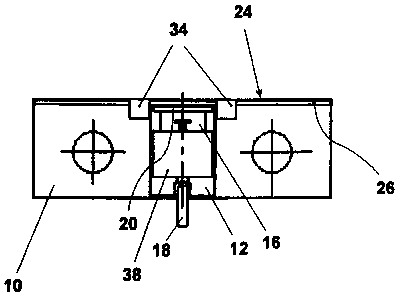
L'invention concerne une résistance de clôture HF qui présente un corps de bride (10) sur lequel est disposée une structure stratifiée plane (16, 18, 20) qui présente sur le côté supérieur (14) d'un substrat (12) une couche résistive (16) qui convertit l'énergie HF en chaleur, une piste (18) de guide d'entrée qui amène l'énergie HF et une piste (20) de guide de raccordement à la masse qui assure la liaison électrique avec un contact de masse prévu sur le corps de bride (10). La piste (18) de guide d'entrée est reliée électriquement à une première extrémité de la couche résistive (16), la piste (20) de guide de raccordement à la masse est reliée électriquement à une deuxième extrémité de la couche résistive (16) opposée à la première extrémité et le substrat (12) repose sur le corps de bride (10) par un côté de pose (22) non tourné vers la structure stratifiée (16, 18, 20). L'agencement est formé en ce que sur un premier côté (24) tourné vers la piste (20) de guide de raccordement à la masse situé sur le substrat (12), le corps de bride (10) est rabattu sur au moins une partie prédéterminée dans une direction parallèle à ce bord (24) ainsi que sur une partie prédéterminée dans la direction perpendiculaire à ce bord (24), de telle sorte que la partie rabattue (26) du corps de bride (10) s'étend dans un espace situé entre un premier plan défini par le côté de pose (22) du substrat (12) et un deuxième plan défini par le côté supérieur (14) du substrat (12). Un côté (28) du substrat (12), qui relie le côté de pose (22) du substrat (12) au côté supérieur (14) du substrat (12) et vers lequel la piste (20) de guide de raccordement de masse située sur le côté supérieur (14) du substrat (12) est tournée, vient buter contre la partie rabattue (26) du corps de bride (10).


Abrégé anglais

In the case of an RF terminating resistor with a flange body (10) and a planar layer structure (16, 18, 20) which is arranged on it and, on an upper face (14) of a substrate (12), has a resistance layer (16) for conversion of RF energy to heat, an input conductor track (18) for supplying RF energy, and an earth connection conductor track (20) for electrical connection to an earth contact on the flange body (12), with the input conductor track (18) being electrically connected to a first end of the resistance layer (16), with the earth connection conductor track (20) being electrically connected to a second end of the resistance layer (16) opposite the first end, and with the substrate (12) having a contact face (22), facing away from the layer structure (16, 18, 20), which rests on the flange body, the arrangement is designed such that, on a first edge (24) which faces the earth connection conductor track (20) on the substrate (12), the flange body (10) is bent around in a direction parallel to this edge (24) over at least one predetermined section, and a predetermined section is bent around in a direction at right angles to this edge (24), such that the bent-around section (26) of the flange body (10) extends in a space between a first plane, defined by the contact face (22) of the substrate (12), and a second plane, defined by the upper face (14) of the substrate (12), with the substrate (12) abutting on the bent-around section (26) of the flange body (10) with a face (28) which connects the contact face (22) of the substrate (12) to the upper face (14) of the substrate (12) and faces the earth connection conductor track (20) on the upper face (14) of the substrate (12).

Revendications

Note : Les revendications sont présentées dans la langue officielle dans laquelle elles ont été soumises.


9
Claims
1. RF terminating resistor with a flange body and a planar
layered structure arranged thereon, which comprises, on an upper
face of a substrate, a resistor layer for converting RF energy
into heat, an input conductor track for supplying RF energy and
an earth connection conductor track for electrical connection to
an earth contact on the flange body, wherein the input conductor
track is electrically connected to a first end of the resistor
layer, the earth connection conductor track is electrically
connected to a second end of the resistor layer opposing the
first end, and the substrate lies on the flange body with a
contact face which faces away from the layered structure,
characterised in that, at a first edge which faces toward the
earth connection conductor track on the substrate, over at least
one predetermined section in a direction parallel to said edge
and a predetermined section in a direction perpendicular to said
edge, the flange body is bent over such that the bent-over
section of the flange body extends into a space between a first
plane defined by the contact face of the substrate and a second
plane defined by the upper face of the substrate, wherein, with
one side which connects the contact face of the substrate to the
upper face of the substrate and towards which the earth
connection conductor track on the upper face of the substrate
faces, the substrate abuts the bent-over section of the flange
body, wherein the bent-over section of the flange body has at
least two noses, the separation of which in the direction
parallel to the first edge of the flange body corresponds to the
width of the substrate, and which extend into a space between
the first plane and the second plane.

10
2. RF terminating resistor according to claim 1, wherein
the bent-over section of the flange body rises from the first
plane at least into the second plane or therebeyond, such that
at least one section of the bent-over section of the flange body
extends in the second plane adjacent to the earth connection
conductor track.
3. RF terminating resistor according to any one of claims 1
or 2, wherein the bent-over section of the flange body has a
length in a direction parallel to the first edge which
corresponds to at least a width of the substrate.
4. RF terminating resistor according to any one of claims
1, 2 or 3, wherein the bent-over section encloses an angle of
90° with the first plane on a side facing toward the substrate.
5. RF terminating resistor according to any one of claims
1, 2, 3 or 4, wherein the bent-over section encloses an angle
with the first plane on a side facing towards the substrate of
less than 90°, in particular 86° to 80°.
6. RF terminating resistor according to any one of claims 1
to 4, wherein an angle between the bent-over section of the
flange body and a perpendicular to the upper face of the
substrate has a value in the range of 4° to 10°.

Description

Note : Les descriptions sont présentées dans la langue officielle dans laquelle elles ont été soumises.


CA 02666483 2009-04-15
WO 2008/071271 PCT/EP2007/009645
RF Terminating Resistor of Flanged Construction
Description
The present invention relates.to an RF terminating
resistor with a flange body and a planar layered structure
arranged thereon, which comprises, on an upper face of a
substrate, a resistor layer for converting RF energy into
heat, an input conductor track for supplying RF energy and
an earth connection conductor track for electrical
connection to an earth contact on the flange body, wherein
the input conductor track is electrically connected to a
first end of the resistor layer, the earth connection
conductor track is electrically connected to a second end
of the resistor layer opposing the first end and the
substrate lies on the flange body with a contact face which
faces away from the layered structure, according to the
preamble of claim 1.
Broadband RF terminating resistors of flanged
construction serve to conduct away large power losses. It
is known to mount a resistor structure on a substrate and
to arrange said substrate on a flange body which represents
an earth contact. In order to create an electrical
connection from the resistor structure to the earth contact
of the flange body, it is necessary to build up an edge
peripheral contact round the substrate or a substrate
through contact to the earth connection. However, both are
complex and costly.
It is an object of the invention to improve an RF
terminating resistor of the aforementioned type with regard
to its design and production and also not to worsen the

p . i
CA 02666483 2009-04-15
WO 2008/071271 2 PCT/EP2007/009645
electrical properties of the RF terminating resistor, but
rather to improve them.
This aim is achieved according to the invention with
an RF terminating resistor of the aforementioned type and
having the characterising features of claim 1. Advantageous
embodiments of the invention are described in the other
claims.
In an RF terminating resistor of the aforementioned
type, it is provided according to the invention that, at a
first edge which faces toward the earth connection
conductor track on the substrate, over at least one
predetermined section in a direction parallel to said edge
and a predetermined section in a direction perpendicular to
said edge, the flange body is bent over such that the bent-
over section of the flange body extends into a space
between a first plane defined by the contact face of the
substrate and a second plane defined by the upper face of
the substrate, wherein, with one side which connects the
contact face of the substrate to the upper face of the
substrate and towards which the earth connection conductor
track on the upper face of the substrate faces, the
substrate abuts the bent-over section of the flange body.
This has the advantage that, in order to produce the
electrical contact between the earth connection conductor
track and the earth contact on the flange body, a costly
edge peripheral contact round one side of the substrate is
not necessary, but rather this electrical contact is
arranged in the second plane of the upper side of the
substrate on which the earth connection conductor track is
arranged on the substrate, can be easily produced by
electrically connecting the earth connection conductor
track to the bent-over section of the flange body.

CA 02666483 2009-04-15
WO 2008/071271 3 PCT/EP2007/009645
An electrical contact between the earth connection
contract track and the bent-over section of the flange body
can be particularly easily achieved in that the bent-over
section of the flange body rises from the first plane at
least into the second plane or therebeyond, such that at
least one section of the bent-over section of the flange
body extends in the second plane adjacent to the earth
connection conductor track.
Suitably, the bent-over section of the flange body has
a length in a direction parallel to the first edge which
corresponds to at least a width of the substrate.
In that the bent-over section of the flange body has
at least two noses, the separation of which in the
direction parallel to the first edge of the flange body
corresponds to the width of the substrate, and which,
starting from the elevation, extend into a space between
the first plane and the second plane, a stop is provided on
both sides for the substrate, fixing a position of the
substrate on the flange body even before the fastening of
the substrate onto the flange body.
Suitably,.the bent-over section encloses an angle of
90 with the first plane on a side facing toward the
substrate.
In order to ensure that the bent-over section touches
the substrate, the bent-over section encloses an angle with
the first plane on a side facing towards the substrate of
less than 90 , in particular 86 to 80 .
The invention will now be described in greater detail
by reference to the drawings, in which:
Fig. 1 shows a preferred embodiment of an RF
terminating resistor according to the invention in a plan
view,

CA 02666483 2009-04-15
WO 2008/071271 4 PCT/EP2007/009645
Fig. 2 shows the RF terminating resistor according to
Fig. 1 in a side view,
Fig. 3 shows a flange body for an RF terminating
resistor according to the invention in a plan view,
Fig. 4 shows the flange body of Fig. 3 in a side view,
Fig. 5 shows the detail Z of Fig. 4, and
Fig. 6 shows the flange body of Fig. 3 in an unrolled
representation.
The preferred embodiment of an RF terminating resistor
of flange construction according to the invention shown in
Figs. 1 and 2 comprises a flange body 10 on which a
substrate 12 is arranged. Arranged on an upper face 14 of
the substrate 12 is a layered structure which comprises a
resistor layer 16 for converting RF energy into heat, an
i5 input conductor track 18 for supplying RF energy and an
earth connection conductor track 20 for electrical
connection to an earth contact on the flange body-10: The
input conductor track 18 is electrically connected to a
first end of the resistor layer 16. The earth connection
conductor track 20 is electrically connected to a second
end of the resistor layer 16 opposing the first end. The
substrate 12 lies with a contact face 22 which faces away
from the layered structure 16, 18, 20 on the flange body
10.
The flange body 10 has an edge 24 wherein the
substrate 12 is arranged with the layered structure 16, 18,
20 mounted thereon on the flange body 10 such that the
earth connection conductor track 20 faces towards said edge
24.
The contact face 22 of the substrate 12 defines a
first plane and the upper face 14 of the substrate 12
defines a second plane.

CA 02666483 2009-04-15
WO 2008/071271 5 PCT/EP2007/009645
As shown also by Figs. 3 to 6, over a predetermined
section in a direction parallel to the edge 24 and over a
predetermined section in a direction perpendicular to the
edge 24, said edge 24 is bent over. In the exemplary
embodiment shown in the figures, the predetermined section
extends parallel to the edge 24 over the whole length of
the edge 24. This predetermined section parallel to the
edge 24 can alternatively extend over just part of the
length of the edge 24, for example, over a length
corresponding to the width of the substrate 12 in a
direction parallel to the edge 24.
The bent-over section 26 of the flange body 10 is
configured and bent over in such a way that the bent-over
section 26 extends at least into the space between the
first and second planes. In the exemplary embodiment shown,
the bent-over section 26 extends completely through the
space between the first and second planes as far as the
second plane and further beyond the second plane. However,
it is also possible for the bent-over section 26 to extend
exactly as far as the second plane or to end within the
space between the first and second planes.
The substrate 12 makes contact with a short face 28,
which connects the upper face 14 of the substrate 12 to the
contact face 22 of the substrate 12, on the bent-over
section 26 of the flange body 10. The short face 28 is the
face of the substrate 12 which faces towards the earth
connection conductor track 20 on the upper face 14 of the
substrate 12. In order to ensure this abutting of the short
face 28 against the bent-over section 26 of the flange body
10 in any event, it is particularly advantageous if the
bent-over section 26 of the flange body 10 is bent over by
more than 90 relative to the flange body 10. This produces
an angle between the bent-over section 26 of the flange

CA 02666483 2009-04-15
WO 2008/071271 6 PCT/EP2007/009645
body 10 and the upper face of the substrate 12 or between
the bent-over section 26 and the plane defined by said
upper face on a side facing towards the substrate 12 of
less than 90 , for example 86 to 80 . Expressed otherwise,
an angle 30 between the bent-over section 26 of the flange
body 10 and a perpendicular 32 to the upper face 14 of the
substrate 12 has a value in the range of 4 to 10 .
Also arranged on the bent-over section 26 of the
flange body 10 are two noses 34 which extend beyond the end
of the bent-over section 26 and.are bent over relative to
the bent-over section 26 by a further angle 36 of, for
example 45 . These noses 34 therefore extend back into the
space between the first and second planes. The spacing
between these noses 34 in a direction parallel to the edge
24 of the flange body 10 corresponds approximately to the
width of the substrate 12 in the direction parallel to the
edge 24. By this means, the position of the substrate 12 on
the flange body 10 and relative to the bent-over section 26
is fixed by positioning between the noses 34 and simplifies
mounting of the substrate 12 on the flange body 10.
The bent-over section 26 of the flange body 10 forms
the earth contact for the earth connection conductor track
20. In that the bent-over section 26 extends into the space
between the first and second planes, electrical contact can
easily be created between the earth connection conductor
track 20 and the bent-over section 26 without complete edge
peripheral contact round the short face 28 of the substrate
12. In the exemplary embodiment shown, the bent-over
section 26 extends above the second plane or the upper face
14 of the substrate 12, so that the electrical contact
between the earth connection conductor track 20 and the
bent-over section 26 of the flange body 10 can be created
directly in one plane, specifically the second plane of the

CA 02666483 2009-04-15
WO 2008/071271 7 PCT/EP2007/009645
upper face 14 of the substrate 12. This simplifies the
creation of the electrical contact and, simultaneously,
improves the electrical properties of the RF terminating
resistor, since the path of the electrical contact is as
short as possible and no longer leads completely round an
edge of the substrate 12.
A covering 38 partially covers the layered structure
16, 18, 20. This covering is made, for example, from the
same material as the substrate 12. The covering 38
therefore has the same dielectric constant as the material
of the substrate 12. This also positively influences the
electrical properties of the RF terminating resistor, since
due to the dielectric (12, 38), that is, the substrate 12
on one side and the covering 38 on the other side, which is
identical on both sides, the electric field is guided close
to the layered structure 16, 18, 20.
Thanks to the improved design of the RF terminating
resistor according to the invention, inexpensive substrates
12, that is substrates without an edge peripheral contact,
can be used. The overall design of the flanged load ensures
the transfer of large power losses whilst maintaining the
best possible broadband RF properties.
The flange body or the flange sheet 10 with the bent-
over section 26 is made entirely from one piece, for
example, a press-bent part. The bent-over section 26 serves
for the earth connection of the resistor structure 14 to
the flange sheet 10. The overall construction including the
substrate structure 12, 16, 18, 20 is intended for a
broadband application with very good RF properties.
In order to produce an electrical connection between
the earth connection conductor track 20 on the substrate 12
and the bent-over section 26 of the flange body 10, so that
the earth contact for the RF terminating resistor is made,

CA 02666483 2009-04-15
WO 2008/071271 8 PCT/EP2007/009645
for example, a solder joint is made from the earth
connection conductor track 20 to the bent-over section 26.
In that the bent-over section 26 extends in particularly
advantageous manner as far as or beyond the upper face 14
of the substrate 12 (second plane), said solder joint can
be made easily, quickly and inexpensively in the second
plane of the upper face 14 of the substrate.12.

Dessin représentatif
Une figure unique qui représente un dessin illustrant l'invention.
États administratifs

2024-08-01 : Dans le cadre de la transition vers les Brevets de nouvelle génération (BNG), la base de données sur les brevets canadiens (BDBC) contient désormais un Historique d'événement plus détaillé, qui reproduit le Journal des événements de notre nouvelle solution interne.

Veuillez noter que les événements débutant par « Inactive : » se réfèrent à des événements qui ne sont plus utilisés dans notre nouvelle solution interne.

Pour une meilleure compréhension de l'état de la demande ou brevet qui figure sur cette page, la rubrique Mise en garde , et les descriptions de Brevet , Historique d'événement , Taxes périodiques et Historique des paiements devraient être consultées.

Historique d'événement

Description Date
Lettre envoyée 2024-05-07
Lettre envoyée 2023-11-07
Représentant commun nommé 2019-10-30
Requête pour le changement d'adresse ou de mode de correspondance reçue 2018-01-12
Accordé par délivrance 2016-01-05
Inactive : Page couverture publiée 2016-01-04
Préoctroi 2015-08-17
Inactive : Taxe finale reçue 2015-08-17
Un avis d'acceptation est envoyé 2015-07-03
Lettre envoyée 2015-07-03
Un avis d'acceptation est envoyé 2015-07-03
Inactive : QS réussi 2015-05-19
Inactive : Approuvée aux fins d'acceptation (AFA) 2015-05-19
Modification reçue - modification volontaire 2015-01-07
Inactive : Dem. de l'examinateur par.30(2) Règles 2014-07-15
Inactive : Rapport - Aucun CQ 2014-06-27
Lettre envoyée 2012-11-05
Requête d'examen reçue 2012-10-16
Exigences pour une requête d'examen - jugée conforme 2012-10-16
Toutes les exigences pour l'examen - jugée conforme 2012-10-16
Inactive : Page couverture publiée 2009-07-31
Inactive : Notice - Entrée phase nat. - Pas de RE 2009-07-09
Inactive : CIB en 1re position 2009-06-13
Demande reçue - PCT 2009-06-12
Inactive : Déclaration des droits - PCT 2009-04-16
Exigences pour l'entrée dans la phase nationale - jugée conforme 2009-04-15
Demande publiée (accessible au public) 2008-06-19

Historique d'abandonnement

Il n'y a pas d'historique d'abandonnement

Taxes périodiques

Le dernier paiement a été reçu le 2015-10-29

Avis : Si le paiement en totalité n'a pas été reçu au plus tard à la date indiquée, une taxe supplémentaire peut être imposée, soit une des taxes suivantes :

  • taxe de rétablissement ;
  • taxe pour paiement en souffrance ; ou
  • taxe additionnelle pour le renversement d'une péremption réputée.

Les taxes sur les brevets sont ajustées au 1er janvier de chaque année. Les montants ci-dessus sont les montants actuels s'ils sont reçus au plus tard le 31 décembre de l'année en cours.
Veuillez vous référer à la page web des taxes sur les brevets de l'OPIC pour voir tous les montants actuels des taxes.

Titulaires au dossier

Les titulaires actuels et antérieures au dossier sont affichés en ordre alphabétique.

Titulaires actuels au dossier
ROSENBERGER HOCHFREQUENZTECHNIK GMBH & CO. KG
Titulaires antérieures au dossier
FRANK WEISS
Les propriétaires antérieurs qui ne figurent pas dans la liste des « Propriétaires au dossier » apparaîtront dans d'autres documents au dossier.
Documents

Pour visionner les fichiers sélectionnés, entrer le code reCAPTCHA :


Pour visualiser une image, cliquer sur un lien dans la colonne description du document. Pour télécharger l'image (les images), cliquer l'une ou plusieurs cases à cocher dans la première colonne et ensuite cliquer sur le bouton "Télécharger sélection en format PDF (archive Zip)" ou le bouton "Télécharger sélection (en un fichier PDF fusionné)".

Liste des documents de brevet publiés et non publiés sur la BDBC .

Si vous avez des difficultés à accéder au contenu, veuillez communiquer avec le Centre de services à la clientèle au 1-866-997-1936, ou envoyer un courriel au Centre de service à la clientèle de l'OPIC.


Description du
Document 
Date
(aaaa-mm-jj) 
Nombre de pages   Taille de l'image (Ko) 
Description 2009-04-14 8 312
Dessins 2009-04-14 2 21
Revendications 2009-04-14 2 78
Dessin représentatif 2009-04-14 1 5
Abrégé 2009-04-14 2 113
Revendications 2015-01-06 2 74
Dessin représentatif 2016-01-04 1 5
Courtoisie - Brevet réputé périmé 2024-06-17 1 529
Rappel de taxe de maintien due 2009-07-08 1 110
Avis d'entree dans la phase nationale 2009-07-08 1 192
Rappel - requête d'examen 2012-07-09 1 125
Accusé de réception de la requête d'examen 2012-11-04 1 175
Avis du commissaire - Demande jugée acceptable 2015-07-02 1 161
Avis du commissaire - Non-paiement de la taxe pour le maintien en état des droits conférés par un brevet 2023-12-18 1 541
Paiement de taxe périodique 2018-11-06 1 26
PCT 2009-04-14 12 310
Correspondance 2009-04-15 2 56
Taxes 2009-10-21 1 36
Taxes 2010-10-18 1 36
Taxe finale 2015-08-16 1 53