Note: Descriptions are shown in the official language in which they were submitted.
CA 02666519 2009-04-15
WO 2008/057392
PCT/US2007/023095
METHODS OF FABRICATING SEMICONDUCTOR DEVICES INCLUDING
IMPLANTED REGIONS FOR PROVIDING LOW-RESISTANCE CONTACT
TO BURIED LAYERS AND RELATED DEVICES
FIELD OF THE INVENTION
[0001] The present invention relates to semiconductor devices, and more
particularly, to semiconductor devices including implanted regions and related
methods of fabrication.
BACKGROUND OF THE INVENTION
[0002] There is a high level of interest in wide bandgap semiconductor
materials such as silicon carbide (2.996 eV for alpha SiC at room temperature)
and
the Group III nitrides (e.g., 3.36 eV for GaN at room temperature) for high
power,
high temperature and/or high frequency applications. These materials,
typically, have
higher electric field breakdown strengths and higher electron saturation
velocities as
compared to gallium arsenide and silicon.
[0003] In order to provide desired properties in semiconductor materials,
it is
frequently desirable to dope a semiconductor layer with impurity atoms (i.e.,
dopants). Doping of semiconductor materials may be performed during and/or
after
material growth. Impurity atoms may be categorized as n-type or p-type
depending
on whether the implanted ions act as donors (which increase the number of
electrons)
or acceptors (which increase the number of holes), respectively, in the doped
material.
The resulting material may be characterized as n-type or p-type depending on
the
predominant type of dopants in the material.
[0004] Ion implantation is a well-known method of doping a semiconductor
layer with impurities. In an ion implantation process, ionized impurity atoms
are
accelerated under high vacuum through an electric field towards a target
layer, where
they become implanted. The number of ions directed at a target layer is
referred to as
the dose, which is typically expressed in ions/cm2. The ions are accelerated
at an
energy level, typically expressed in electron-volts (eV). The distribution of
ions in
the implanted layer depends on the dose and energy of the implant, sometimes
referred to as the implant conditions, as well as the type of ions implanted,
the type of
material the ions are implanted into, the angle of the implants, and other
factors. The
1
CA 02666519 2009-04-15
WO 2008/057392
PCT/US2007/023095
implanted ions typically form a concentration distribution that has a peak
concentration at a particular depth (i.e., the "implant range").
[0005] Ion implantation may be useful for selective doping of crystalline
material in order to form desired regions in the material, such as p-n
junctions, highly
conductive contact regions, field spreading regions, etc. Typically, after
impurities
are implanted into a semiconductor layer, it may be desirable to anneal the
implanted
impurities at a high temperature, i.e., a so-called activation anneal. An
activation
anneal may repair damage caused by the implantation of high-energy ions into
the
semiconductor lattice. Implant damage may include, for example, broken and/or
rearranged chemical bonds within the semiconductor lattice. The activation
anneal
may also assist implanted impurity ions in finding a suitable site in the
crystal lattice
at which the ions may appropriately act as acceptors and/or donors. However,
for
some semiconductor materials, the temperature at which appreciable lattice
damage
repair may occur may be above the temperature at which the material will
dissociate
at normal ambient pressures. As such, it is known to provide a stable capping
layer
on an implanted semiconductor layer during the activation anneal. The material
of the
capping layer may be stable at high temperatures, and may not react with the
underlying implanted semiconductor layer.
SUMMARY OF THE INVENTION
[0006] According to some embodiments of the present invention, a method
of
fabricating a semiconductor device includes forming a first semiconductor
layer of a
first conductivity type and having a first dopant concentration, and forming a
second
semiconductor layer on the first semiconductor layer. The second semiconductor
layer has a second dopant concentration that is less than the first dopant
concentration.
Ions are implanted into the second semiconductor layer to form an implanted
region
of the first conductivity type extending through the second semiconductor
layer to
contact the first semiconductor layer. A first electrode is formed on the
implanted
region of the second semiconductor layer, and a second electrode is formed on
a non-
implanted region of the second semiconductor layer that is spaced apart from
the
implanted region.
[0007] In some embodiments, the first semiconductor layer and the second
semiconductor layer may be a Group III-nitride material. The first and second
2
CA 02666519 2009-04-15
WO 2008/057392
PCT/US2007/023095
semiconductor layers may be formed on a silicon carbide (SiC) substrate. In
addition,
the implanted ions may be silicon (Si), sulfur (S) and/or oxygen (0) ions.
[0008] In other embodiments, a protective layer may be formed on the
second
semiconductor layer prior to implanting the ions. The ions may thereby be
implanted
into the second semiconductor layer through the protective layer. After
implanting
the ions, the first and second semiconductor layers and the protective layer
may be
annealed to activate the implanted ions. In some embodiments, the protective
layer
may be silicon nitride (SiN), silicon dioxide (Si02), and/or silicon
oxynitride (SiON).
In other embodiments, the protective layer may be a high purity nitride (HPN)
layer.
[0009] In some embodiments, in forming the first electrode, an opening
may
be formed in the protective layer after annealing to expose the implanted
region of the
second semiconductor layer. An ohmic contact may be formed in the opening on
the
exposed implanted region. In addition, a second opening in may be formed in
the
protective layer to expose a non-implanted region of the second semiconductor
layer,
and the second electrode may be formed in the second opening.
[0010] In other embodiments, the first and second semiconductor layers
may
be gallium nitride (GaN). A first protective layer may be formed on the second
semiconductor layer, and a second protective layer may be formed on the first
protective layer. The first protective layer may be a Group III-nitride
including
aluminum, and the second protective layer may be a high purity nitride (HPN).
[0011] In some embodiments, the ions may be implanted into the second
semiconductor layer to form the implanted region extending through the second
semiconductor layer and at least partially into the protective layer and/or
the first
semiconductor layer. Accordingly, the distribution of implanted dopants may
extend
at least partially into the protective layer and/or at least partially into
the first
semiconductor layer. The implanted region may have a peak dopant concentration
in
the second semiconductor layer. For example, the implanted region may have a
peak
dopant concentration of about 5x10² ions/cm3.
[0012] In other embodiments, the ions may be implanted into the second
semiconductor layer to provide a distribution of implanted dopants having a
substantially uniform concentration throughout the implanted region. For
example,
depending on a thickness of the second semiconductor layer and/or other
layers, a
plurality of doses and/or implantation energies may be selected to provide the
substantially uniform concentration.
3
CA 02666519 2009-04-15
WO 2008/057392
PCT/US2007/023095
[0013] In some embodiments, to provide a distribution of implanted
dopants
having a substantially uniform concentration, ions of the first conductivity
type may
be implanted into the second semiconductor layer at a first dose and at a
first
implantation energy, and then ions of the first conductivity type may be
implanted
into the second semiconductor layer at a second dose and at a second
implantation
energy. For example, the first dose may be about 0.5x10¹⁵to about 2.5x10¹⁵
ions/cm2,
and the first implantation energy may be about 160keV. Also, the second dose
may
be about 0.8x10'5 to about 5x10¹⁵ ions/cm2, and the second implantation energy
may
be about 260keV. In addition, in some embodiments, the ions of the first
conductivity
type may be further implanted into the second semiconductor layer at a third
dose and
at a third implantation energy. For instance, the third dose may be about
0.5x10¹⁵to
about 3.7x10¹⁵ ions/cm2, and the third implantation energy may be about
360keV.
[0014] In other embodiments, the first semiconductor layer and the second
semiconductor layer may be a same material. In some embodiments, the second
semiconductor layer may be an undoped layer. In other embodiments, the second
semiconductor layer may have a same and/or opposite conductivity type as the
first
semiconductor layer.
[0015] In some embodiments, the first semiconductor layer and/or the
second
semiconductor layers may be an epitaxial layer. For example, the first
semiconductor
layer may be epitaxially grown to have the first dopant concentration on a
substrate.
Also, the second semiconductor layer may be epitaxially grown to have the
second
dopant concentration on the first semiconductor layer.
[0016] In other embodiments, the first electrode may be an ohmic contact.
In
addition, in some embodiments, a lateral distance between the second electrode
and
the implanted region may be less than a lateral distance between the second
electrode
and the first electrode. For example, the lateral distance between the second
electrode
and the implanted region may be less than about 1 micron (j.tm).
[0017] In some embodiments, the first electrode may be a cathode contact
formed on the implanted region of the second semiconductor layer. Also, the
second
electrode may be an anode contact formed on the non-implanted region of the
second
semiconductor layer spaced apart from the implanted region. In some
embodiments,
the first semiconductor layer and/or the second semiconductor layer may have a
thickness of about 100 nm to about 500 nm.
4
CA 02666519 2015-04-08
[0018] In other embodiments, the first electrode may be a source/drain
contact
formed on the implanted region of the second semiconductor layer. Also, the
second
electrode may be a gate contact formed on the non-implanted region of the
second
semiconductor layer spaced apart from the implanted region. In some
embodiments,
the gate contact and the source/drain contact may be formed in a same
metallization
process. Also, in some embodiments, a bandgap of the second semiconductor
layer
may be greater than a bandgap of the first semiconductor layer.
[0019] According to other embodiments of the present invention, a
semiconductor device includes a first semiconductor layer of a first
conductivity type
and having a first dopant concentration, a second semiconductor layer on the
first
semiconductor layer and having a second dopant concentration that is less than
the
first dopant concentration, an implanted region in the second semiconductor
layer
including a distribution of implanted dopants of the first conductivity type
extending
through the second semiconductor layer to contact the first semiconductor
layer, a
first electrode on the implanted region of the second semiconductor layer, and
a
second electrode on a non-implanted region of the second semiconductor layer
that is
spaced apart from the implanted region.
[0019a] In accordance with an aspect of an embodiment, there is provided a
method of fabricating a semiconductor device, the method comprising: forming a
first
semiconductor layer of a first conductivity type; forming a second
semiconductor
layer on the first semiconductor layer, the second semiconductor layer having
a lower
conductivity than that of the first semiconductor layer; implanting ions into
the second
semiconductor layer to form an implanted region of the first conductivity type
extending through the second semiconductor layer to contact the first
semiconductor
layer, wherein the implanted region comprises a distribution of implanted
dopants
having an implanted dopant concentration of at least about 5x10² ions/cm3 at
a depth
within the implanted region of at least about 1500 Angstroms; forming a first
electrode on the implanted region of the second semiconductor layer; and
forming a
second electrode on a non-implanted region of the second semiconductor layer
that is
spaced apart from the implanted region.
CA 02666519 2015-04-08
[0019b] In accordance with another aspect of an embodiment, there is
provided
a semiconductor device, comprising: a first semiconductor layer of a first
conductivity
type and having a first dopant concentration; a second semiconductor layer on
the first
semiconductor layer and having a second dopant concentration that is less than
the
first dopant concentration; an implanted region in the second semiconductor
layer
including a distribution of implanted dopants of the first conductivity type
extending
through the second semiconductor layer to contact the first semiconductor
layer,
wherein the implanted region comprises a distribution of implanted dopants
having an
implanted dopant concentration of at least about 5x10²⁰ ions/cm3 at a depth
within the
implanted region of at least about 1500 Angstroms; a first electrode on the
implanted
region of the second semiconductor layer; and a second electrode on a non-
implanted
region of the second semiconductor layer that is spaced apart from the
implanted
region.
BRIEF DESCRIPTION OF THE DRAWINGS
[0020] The accompanying drawings, which are included to provide a further
understanding of the invention and are incorporated in and constitute a part
of this
application, illustrate certain embodiment(s) of the invention. In the
drawings:
[0021] Figures 1A-1F are cross-sectional views illustrating fabrication
of
semiconductor devices according to embodiments of the present invention; and
[0022] Figure 2 is a graph illustrating simulation results for the
implantation
of silicon into gallium nitride structures according to some embodiments of
the
present invention.
DETAILED DESCRIPTION OF EMBODIMENTS OF THE INVENTION
[0023] Embodiments of the present invention now will be described more
fully hereinafter with reference to the accompanying figures, in which
embodiments
of the invention are shown. This invention may, however, be embodied in many
different forms and should not be construed as limited to the embodiments set
forth
herein; rather, these embodiments are provided so that this disclosure will be
thorough
5a
CA 02666519 2009-04-15
WO 2008/057392
PCT/US2007/023095
and complete, and will fully convey the scope of the invention to those
skilled in the
art. Like numbers refer to like elements throughout.
[0024] It will be understood that when an element such as a layer, region
or
substrate is referred to as being "on" or extending "onto" another element, it
can be
directly on or extend directly onto the other element or intervening elements
may also
be present. In contrast, when an element is referred to as being "directly on"
or
extending "directly onto" another element, there are no intervening elements
present.
It will also be understood that when an element is referred to as being
"connected" or
"coupled" to another element, it can be directly connected or coupled to the
other
element or intervening elements may be present. In contrast, when an element
is
referred to as being "directly connected" or "directly coupled" to another
element,
there are no intervening elements present. It will also be appreciated by
those of skill
in the art that references to a structure or feature that is disposed
"adjacent" another
feature may have portions that overlap or underlie the adjacent feature.
[0025] It will also be understood that, although the terms first, second,
etc.
may be used herein to describe various elements, these elements should not be
limited
by these terms. These terms are only used to distinguish one element from
another.
For example, a first element could be termed a second element, and, similarly,
a
second element could be termed a first element, without departing from the
scope of
the present invention.
[0026] Furthermore, relative terms, such as "lower" or "below" and
"upper" or
"above" may be used herein to describe one element's relationship to another
element
as illustrated in the Figures. It will be understood that relative terms are
intended to
encompass different orientations of the device in addition to the orientation
depicted
in the Figures. For example, if the device in one of the figures is turned
over,
elements described as being on the "lower" side of other elements would then
be
oriented on "upper" sides of the other elements. The exemplary term "lower",
can
therefore, encompasses both an orientation of "lower" and "upper," depending
of the
particular orientation of the figure. Similarly, if the device in one of the
figures is
turned over, elements described as "below" or "beneath" other elements would
then be
oriented "above" the other elements. The exemplary terms "below" or "beneath"
can,
therefore, encompass both an orientation of above and below.
[0027] The terminology used in the description of the invention herein is
for
the purpose of describing particular embodiments only and is not intended to
be
6
CA 02666519 2009-04-15
WO 2008/057392
PCT/US2007/023095
limiting of the invention. As used in the description of the invention and the
appended claims, the singular forms "a", "an " and "the" are intended to
include the
plural forms as well, unless the context clearly indicates otherwise. It will
also be
understood that the term "and/or" as used herein refers to and encompasses any
and
all possible combinations of one or more of the associated listed items. It
will be
further understood that the terms "comprises" and/or "comprising," when used
in this
specification, specify the presence of stated features, integers, steps,
operations,
elements, and/or components, but do not preclude the presence or addition of
one or
more other features, integers, steps, operations, elements, components, and/or
groups
thereof.
[0028] Embodiments of the invention are described herein with reference
to
cross-section illustrations that are schematic illustrations of idealized
embodiments
(and intermediate structures) of the invention. The thickness of layers and
regions in
the drawings may be exaggerated for clarity. Additionally, variations from the
shapes
of the illustrations as a result, for example, of manufacturing techniques
and/or
tolerances, are to be expected. Thus, embodiments of the invention should not
be
construed as limited to the particular shapes of regions illustrated herein
but are to
include deviations in shapes that result, for example, from manufacturing. For
example, an implanted region illustrated as a rectangle will, typically, have
rounded
or curved features and/or a gradient of implant concentration at its edges
rather than a
discrete change from implanted to non-implanted region. Likewise, a buried
region
formed by implantation may result in some implantation in the region between
the
buried region and the surface through which the implantation takes place.
Thus, the
regions illustrated in the figures are schematic in nature and their shapes
are not
intended to illustrate the actual shape of a region of a device and are not
intended to
limit the scope of the invention.
[0029] Unless otherwise defined, all terms (including technical and
scientific
terms) used herein have the same meaning as commonly understood by one of
ordinary skill in the art to which this invention belongs. It will be further
understood
that terms used herein should be interpreted as having a meaning that is
consistent
with their meaning in the context of this specification and the relevant art
and will not
be interpreted in an idealized or overly formal sense unless expressly so
defined
herein.
7
CA 02666519 2009-04-15
WO 2008/057392
PCT/US2007/023095
[0030] Some embodiments of the present invention may be particularly well
suited for use in Group III-nitride based devices. As used herein, the term
"Group III
nitride" refers to those semiconducting compounds formed between nitrogen and
the
elements in Group III of the periodic table, usually aluminum (Al), gallium
(Ga),
and/or indium (In). The term also refers to ternary and quaternary compounds
such as
AlGaN and AlInGaN. As is well understood by those in this art, the Group III
elements can combine with nitrogen to form binary (e.g., GaN), ternary (e.g.,
AlGaN,
AlInN), and quaternary (e.g., AlInGaN) compounds. These compounds all have
empirical formulas in which one mole of nitrogen is combined with a total of
one
mole of the Group III elements. Accordingly, formulas such as AlõGai.õN where
0
x 1 are often used to describe them.
[0031] Some embodiments of the present invention provide methods for
forming implanted regions that extend through a lower-conductivity
semiconductor
layer to facilitate ohmic contact to a buried higher-conductivity
semiconductor layer.
More particularly, ions are implanted into the lower-conductivity
semiconductor layer
to form the implanted region extending through the lower-conductivity
semiconductor
layer to contact the higher-conductivity semiconductor layer.
[0032] Structures that may utilize implanted regions according to some
embodiments of the present invention may include a conductive channel layer
that is
buried under a higher-bandgap barrier layer, such as high electron mobility
transistors
(HEMTs). Suitable structures for GaN-based HEMTs that may utilize embodiments
of the present invention are described, for example, in commonly assigned U.S.
Patent
6,316,793 and U.S. Patent Publication No. 2002/0066908A1 filed July 12, 2001
and
published June 6, 2002, for "ALUMINUM GALLIUM NITRIDE/GALLIUM
NITRIDE HIGH ELECTRON MOBILITY TRANSISTORS HAVING A GATE
CONTACT ON A GALLIUM NITRIDE BASED CAP SEGMENT AND
METHODS OF FABRICATING SAME", U.S. Provisional Application Serial No.
60/290,195 filed May 11, 2001 for "GROUP III NITRIDE BASED HIGH
ELECTRON MOBILITY TRANSISTOR (HEMT) WITH BARRIER/SPACER
LAYER", United States Patent Publication No. 2002/0167023A1 to Smorchkova et
al., published November 14, 2002, entitled "GROUP-III NITRIDE BASED HIGH
ELECTRON MOBILITY TRANSISTOR (HEMT) WITH BARRIER/SPACER
LAYER", United States Patent Application Serial No. 10/617,843 filed July 11,
2003
8
CA 02666519 2015-04-08
for "NITRIDE-BASED TRANSISTORS AND METHODS OF FABRICATION
THEREOF USING NON-ETCHED CONTACT RECESSES", and U.S. Patent
Application Serial No. 11/302,062 filed December 13, 2005 for
"SEMICONDUCTOR DEVICES INCLUDING IMPLANTED REGIONS AND
PROTECTIVE LAYERS AND METHODS OF FORMING THE SAME".
[0033] A particular structure that may utilize implanted regions
according to
some embodiments of the present invention may include a highly conductive
layer
that is buried under a less conductive and/or insulating layer. For example, a
n+/n-
metal-semiconductor (M-S) diode may include an undoped or low-doped n- layer
on
top of a highly conductive n+ layer. The n- layer may provide good Schottky
behavior, and may provide a predetermined distance between the anode and the
highly conductive n+ layer. However, providing a cathode contact to the highly
conductive buried n+ layer may require recessing through the n- layer, which
may be
difficult and/or non-repeatable when both the n- and n+ layers are formed of a
same
material. Accordingly, in some embodiments of the present invention, ions are
implanted into the n- layer to form an implanted region extending through the
n- layer
to provide ohmic contact to the highly conductive buried n+ layer.
[0034] Fabrication of structures according to some embodiments of the
present invention is schematically illustrated in Figures 1A-1F. As seen in
Figure
1A, a substrate 10 is provided on which nitride based devices may be formed.
In
particular embodiments of the present invention, the substrate 10 may be a
semi-
insulating silicon carbide (SiC) substrate that may be, for example, 4H
polytype of
silicon carbide. Other silicon carbide candidate polytypes include the 3C, 6H,
and
15R polytypes. The term "semi-insulating" is used in a relative rather than
absolute
sense. In particular embodiments of the present invention, the silicon carbide
bulk
crystal has a resistivity equal to or higher than about lx105 a-cm at room
temperature.
[0035] Optional buffer, nucleation and/or transition layers (not shown)
may be
provided on the substrate 10. For example, an MN buffer layer may be provided
to
provide an appropriate crystal structure transition between the silicon
carbide
substrate and the remainder of the device. Additionally, strain balancing
transition
layer(s) may also be provided as described, for example, in commonly assigned
United States Patent Publication 2003/0102482A1 entitled "STRAIN BALANCED
9
CA 02666519 2015-04-08
NITRIDE HETROJUNCTION TRANSISTORS AND METHODS OF
FABRICATING STRAIN BALANCED NITRIDE HETEROJUNCTION
TRANSISTORS, and United States Provisional Patent Application Serial No.
60/337,687, filed December 3, 2001 and entitled "STRAIN BALANCED NITRIDE
HETEROJUNCTION TRANSISTOR".
[0036] Silicon carbide has a much closer crystal lattice match to Group
III
nitrides than does sapphire (A1203), which is a very common substrate material
for
Group III nitride devices. The closer lattice match may result in Group III
nitride
films of higher quality than those generally available on sapphire. Silicon
carbide
also has a very high thermal conductivity so that the total output power of
Group III
nitride devices on silicon carbide is, typically, not as limited by thermal
dissipation of
the substrate as in the case of the same devices formed on sapphire. Also, the
availability of semi-insulating silicon carbide substrates may provide for
device
isolation and reduced parasitic capacitance. Appropriate SiC substrates are
manufactured by, for example, Cree, Inc., of Durham, N.C., the assignee of the
present invention, and methods for producing are described, for example, in U.
S.
Patent Nos. Re. 34,861; 4,946,547; 5,200,022; and 6,218,680. Similarly,
techniques
for epitaxial growth of Group III nitrides have been described in, for
example, U. S.
Patent Nos. 5,210,051; 5,393,993; 5,523,589; and 5,292,501.
[0037] Although silicon carbide may be used as a substrate material,
embodiments of the present invention may utilize any suitable substrate, such
as
sapphire, aluminum nitride, aluminum gallium nitride, gallium nitride,
silicon, GaAs,
LGO, ZnO, LAO, InP and the like. In some embodiments, an appropriate buffer
layer
also may be formed. Furthermore, in some embodiments, the substrate may be
removed after epitaxial growth, and the epitaxial layers may be bonded to a
carrier
substrate.
[0038] Returning to Figure 1A, a relatively high-conductivity
semiconductor
layer is formed on the substrate 10, for example, as a channel layer 20. The
channel
layer 20 may be epitaxially grown on the substrate 10 to have a desired
conductivity
type and/or dopant concentration. For example, in some embodiments, the
channel
layer 20 may be an n-type layer having a dopant concentration of about 1 x
1019
CA 02666519 2009-04-15
WO 2008/057392
PCT/US2007/023095
ions/cm3. The channel layer 20 may also be deposited on the substrate 10 using
buffer layers, transition layers, and/or nucleation layers as described above.
The
channel layer 20 and/or buffer nucleation and/or transition layers may be
deposited by
MOCVD or by other techniques known to those of skill in the art, such as MBE
or
HVPE . In some embodiments of the present invention, the channel layer 20 is a
Group III-nitride layer, such as AlõGalN where 0 x < 1. In certain embodiments
of the present invention, x = 0, indicating that the channel layer 20 is GaN.
The
channel layer 20 may also be other Group III-nitrides layers, such as InGaN,
AlInGaN, or the like.
[0039] Still referring to Figure 1A, a lower-conductivity semiconductor
layer,
referred to hereinafter as a surface layer 22, is formed on the channel layer
20. The
surface layer 22 has a dopant concentration that is less than the dopant
concentration
of the channel layer 20. The surface layer 22 may be epitaxially grown on the
channel layer 20 to have a desired conductivity type and/or dopant
concentration. For
example, the surface layer 22 may be an undoped ("unintentionally doped")
layer,
and/or may have the same and/or opposite conductivity type as the channel
layer 20.
In some embodiments of the present invention, the surface layer 22 is also a
Group
III-nitride layer, such as AlõGai_õN where 0 x < 1. The surface layer 22 may
also be
other Group III-nitrides layers, such as InGaN, AlInGaN, or the like. In
addition, the
channel layer 20 and the surface layer 22 may be formed of the same material.
[0040] Accordingly, in some embodiments of the present invention, the
channel layer 20 and the surface layer 22 may provide a highly-conductive
layer
buried under a less-conductive and/or insulating layer, for example, for use
in a metal-
semiconductor or Schottky diode. For example, the channel layer 20 may be a
highly-
doped n-type GaN layer with a dopant concentration of about 1 x 10¹⁹ ions/cm3
or
higher, and the surface layer 22 may be a low-doped or undoped n-type GaN
layer
with a dopant concentration of less than about 1 x 10¹⁹ ions/cm3. The channel
layer
20 and/or the surface layer 22 may be formed to a thickness of about 100 nm to
about
500 nm. Accordingly, the surface layer 22 may provide a controllable Schottky
contact for an electrode 32 to be formed in a subsequent process.
[0041] In other embodiments of the present invention, the channel layer
20
and the surface layer 22 may be selected to provide a heterojunction at the
interface
between the channel and surface layers, for example, for use in a HEMT device.
As
11
CA 02666519 2015-04-08
such, the channel layer 20 may have a bandgap that is less than the bandgap of
the
surface layer 22, which may correspond to the barrier layer in a HEMT device.
The
channel layer 20 may also have a larger electron affinity than the surface
layer 22.
The channel layer 20 may include a multi-layer structure, such as a
superlattice and/or
combinations of GaN, AlGaN, or the like. The surface layer 22 may include
AlGaN,
AlInGaN and/or AN or combinations of layers thereof. In some embodiments of
the
present invention, the aluminum concentration of the surface layer 22 is
greater than
about 10%. However, in other embodiments of the present invention, the surface
layer 22 may include AlGaN with an aluminum concentration of between about 5%
and about 100%. The surface layer 22 may be thick enough and may have a high
enough Al composition and doping to induce a significant carrier concentration
at the
interface between the channel layer 20 and the surface layer 22 through
polarization
effects when the surface layer 22 is buried under ohmic contact metal. Also,
the
surface layer 22 may be thick enough to reduce or minimize scattering of
electrons in
the channel due to ionized impurities deposited at the interface between the
surface
layer 22 and a protective layer 24 (as shown in Figure 1B). In certain
embodiments,
the channel layer 20 may be undoped and may be grown to a thickness of greater
than
about 2 nm. Also, the surface layer 22 may be undoped or doped with an n-type
dopant, and may be grown to a thickness of about 0.1 nm to about 10 nm.
However,
the surface layer 22 should not be so thick as to cause cracking or
substantial defect
formation therein. HEMT structures suitable for use with some embodiments of
the
present invention are further described in commonly assigned U.S. Patent
Application
Serial No. 11/302,062 entitled "SEMICONDUCTOR DEVICES INCLUDING
IMPLANTED REGIONS AND PROTECTIVE LAYERS AND METHODS OF
FORMING THE SAME" filed December 13, 2005.
[0 0 42] Referring now to Figure 1B, a protective layer 24 is formed on the
surface layer 22. The protective layer 24 may be silicon nitride (SixNy),
silicon
dioxide (SiO2) and/or another suitable protective material, such as silicon
oxynitride
(SiON). It will be understood that the terms "SixNy," "SiN" and "silicon
nitride" are
used herein interchangeably to refer to both stoichiometric and non-
stoichimetric
silicon nitride. Other materials may also be utilized for the protective layer
24. For
example, the protective layer 24 could also include magnesium oxide, scandium
oxide, aluminum oxide and/or aluminum oxynitride. Furthermore, the protective
12
CA 02666519 2009-04-15
WO 2008/057392
PCT/US2007/023095
layer 24 may be a single layer or multiple layers of uniform and/or non-
uniform
composition. The material of the protective layer 24 may have appropriate
interface
characteristics, and may be capable of withstanding relatively high
temperatures. In
addition, in some embodiments, the protective layer 24 may be capable of being
removed without significantly damaging the underlying surface layer 22.
[0043] In general, the protective layer 24 may be a dielectric layer that
has a
relatively high breakdown field strength and that provides a relatively low
interface
trap density at the interface with an underlying Group III-nitride layer, such
as the
surface layer 22. The protective layer 24 may have a high etch selectivity
with
respect to the material of the surface layer 22, and may not be reactive to
the material
of the surface layer 22. Moreover, the protective layer 24 may have a
relatively low
level of impurities therein. For example, the protective layer 24 may have a
relatively
low level of hydrogen and other impurities, including oxygen, carbon, fluorine
and
chlorine. In addition, the protective layer 24 may be stable at relatively
high
temperatures (e.g. >1000 C) in order to withstand high annealing temperatures
used
in subsequent process steps.
[0044] In particular embodiments of the present invention, the protective
layer
24 is SiN. The SiN may be formed for example by Low Pressure Chemical Vapor
Deposition (LPCVD) and/or Metal-Organic Chemical Vapor Deposition (MOCVD).
The SiN layer may be stoichiometric (i.e. the ratio of silicon to nitrogen in
the
material is about 3:4). The stoichiometry of a SiN layer may be adjusted, for
example, by adjusting the relative flow rates of SiH4 and NH3 source gases in
a CVD
process. Moreover, when formed at relatively high temperatures, CVD-grown SiN
tends to be stoichiometric.
[0045] The stoichiometry of a SiN layer may also affect the index of
refraction of the layer. In certain embodiments of the present invention, a
SiN
protective layer 24 may have an index of refraction at a 633 nm wavelength of
from
about 1.6 to about 2.2. In particular embodiments, the index of refraction of
a SiN
protective layer 24 is 1.98 0.05 as measured by ellipsometry. Stoichiometric
SiN
may also be characterized by its etch rate in a buffered oxide etch (BOE). For
example, the etch rate of stoichiometric SiN in BOE is nearly zero (i.e., less
than
about lnanometer/minute).
[0046] In some embodiments, the protective layer 24 may be Si02. The Si02
may be formed by LPCVD and/or MOCVD and may be stoichiometric. In certain
13
CA 02666519 2015-04-08
embodiments of the present invention, an Si02 protective layer may have an
index of
refraction at a 633 nm wavelength of from about 1.36 to about 1.56. In
particular
embodiments, the index of refraction of an Si02 protective layer is 1.46
0.03 as
measured by ellipsometry.
[0047] When the protective layer 24 includes silicon nitride, the
protective
layer 24 may have impurity levels at or below the levels shown in Table 1, as
measured by secondary ion mass spectroscopy (SIMS) with a Cs ion beam.
TABLE 1
Element Concentration (cm
3)
4X10²¹
0 3X10"
7X107
lx1016
CL 4x10¹⁶
[0048] The protective layer 24 may be blanket formed on the surface layer
22.
Typically, the protective layer 24 may have a thickness in the range of about
100 nm,
however, other thickness layers may also be utilized. For example, the
protective
layer 24 should be sufficiently thick so as to protect the underlying layer
during a
subsequent impurity activation anneal. Layers as thin as two or three
monolayers may
be sufficient for such purposes. However, in general, the protective layer 24
may
have a thickness of from about 10 nm to about 500nm.
[0049] The protective layer 24 may include a high purity nitride (HPN)
layer,
such as the high purity SiN layer described in U.S. Patent Application Serial
No.
11/286,805 entitled "GROUP III NITRIDE SEMICONDUCTOR DEVICES WITH
SILICON NITRIDE LAYERS AND METHODS OF MANUFACTURING SUCH
DEVICES" filed November 23, 2005. In particular, pursuant to certain
embodiments
of the present invention, an in situ grown SiN protective layer 24 may be
grown at
relatively high temperatures (e.g., above about 700 C). In particular
embodiments,
the SiN layers may be grown at a temperature in the range of about 900 - 1000
C.
Such high temperature growth may also facilitate reducing the impurity levels
in the
SiN layer and at the interface between a Group III nitride layer and the SiN
layer.
14
CA 02666519 2009-04-15
WO 2008/057392
PCT/US2007/023095
Additionally, high growth rates may be employed which may facilitate reducing
the
levels of background reactor impurities incorporated into the SiN layer. For
example,
in certain embodiments of the present invention, the SiN layer(s) may be grown
at a
growth rate of at least about 0.2 microns/hour. In certain specific
embodiments, the
growth rate may be about 2 microns/hour.
[0050] Forming the SiN layer in situ may also reduce the levels of
impurities
that are incorporated into the top surface of the uppermost Group III nitride
layer
and/or into the SiN layer itself. In particular, when the device is removed
from the
reactor and the SiN layer is formed via a post-MOCVD growth process such as,
for
example, sputtering or PECVD, a number of different mechanisms may introduce
impurities. For example, as discussed in detail in U.S. Patent No. 6,498,111,
if
hydrogen is present in an MOCVD reactor during the growth of a Group III
nitride
layer, the hydrogen may tend to incorporate into the Group III nitride layer
during
cooling of the reactor following growth. Likewise, exposure of the device to
the
atmosphere upon removal from the reactor may allow for incorporation of oxygen
atoms, and various other impurities may be introduced, particularly adjacent
the outer
surfaces of the device, as a result of handling of the device and/or chemical
cleaning
of the device. Impurities may also be added if post-growth processing such as
wet
etching, electrode deposition, annealing steps, etc. are performed prior to
deposition
of the SiN protective/passivation layer. These impurities may change the
surface
states at the interface between the Group III nitride layer and the SiN layer
in ways
that may be undesirable and/or difficult to control/reproduce. For example,
the
presence of impurities can increase trapping at the interface between the SiN
layer
and the underlying Group III nitride layer, thereby increasing the sheet
resistance of
the channel.
[0051] In certain embodiments of the present invention, high purity
silane
(SiI-14) may be used as a source gas in the growth of the SiN layer(s). As is
known to
persons of skill in the art, silane is often used as a source for silicon
dopants in the
growth of n-doped Group III nitride layers. Typically, diluted silane gas is
used in
such applications as it is less expensive and easier to use than pure silane,
which may
be highly combustible. The use of such pure silane may facilitate reducing the
level
of impurities at, for example, the interface between the Group III nitride
layer and the
SiN layer and/or within the SiN layer, which may, in certain circumstances,
improve
the performance and/or reproducibility of the device. In particular, the
higher quality
CA 02666519 2009-04-15
WO 2008/057392
PCT/US2007/023095
(i.e., more pure) SiN layer may help reduce or minimize trapping within the
body of
the insulative layer, thereby providing a higher breakdown critical field.
When such a
pure silane gas source is included with the reactor, it may still be desirable
to include
a diluted silane source as well, so that diluted silane gas may be used as the
dopant
gas source during the growth of, for example, an n-doped or co-doped Group III
nitride layer.
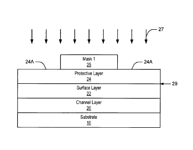
[0052] Referring still to Figure 1B, a mask 25 is formed on the
protective
layer 24. The mask 25 may include photoresist or any other suitable mask
material,
such as SiN and/or Si02. The mask may have a thickness selected to block
implanted
ions. For example, when the protective layer 24 comprises SiN, the mask 25 may
include an oxide such as Si02, and vice-versa.
[0053] Windows are opened in the mask 25 to expose surface portions 24A
of
the protective layer 24, and impurity ions 27 are implanted through the
windows into
the protective layer 24 such that at least a portion of the implanted ions are
implanted
through the protective layer 24 and come to rest within the surface layer 22.
In
addition, some of the implanted ions may come to rest within the channel layer
20.
The implanted ions may form a distribution profile having a peak dopant
concentration in the surface layer 22 between the protective layer 24 and the
channel
layer 20. However, the implant peak may also be formed away from (i.e., above
or
below) the interface 29 between the protective layer 24 and the surface layer
22.
Accordingly, as shown in Figure 1C, an implanted region 31 may be formed
extending through the surface layer 22 to contact the channel layer 20. In
addition, in
some embodiments, the implanted region 31 may extend at least partially into
the
protective layer 24 and/or the channel layer 20.
[0054] The implant conditions may be selected to provide an implanted
region
31 having a peak dopant concentration of lx1018 ions/cm3 or greater. For
example, in
some embodiments, the dose and energy of the implants may be selected to
provide a
peak dopant concentration of about 5x10² ions/cm3in the implanted region 31.
The
implant conditions may also be selected to provide a distribution of implanted
dopants
having a substantially uniform concentration throughout the implanted region
31 of
the surface layer 22. For instance, the implant process may include multiple
implant
steps to provide a relatively uniform profile of implanted dopants throughout
the
implanted region 31. As such, the number of implant steps may depend on the
thickness of the protection layer 24 and/or the surface layer 22 so that the
implanted
16
CA 02666519 2009-04-15
WO 2008/057392
PCT/US2007/023095
region 31 may contact the channel layer 20. For example, the implant process
may
include a first implant step performed under a first set of implant
conditions, and a
subsequent implant step performed under a second set of implant conditions.
However, more than two implant steps may be performed to provide an implanted
region 31 having a substantially uniform dopant concentration, as will be
discussed
below with reference to Figure 2.
[0055] In some embodiments, the implantation may be performed at room
temperature. The implant energies and/or doses may be selected to provide an
implant profile that achieves a desired sheet resistivity and/or permits
fabrication of
low resistivity ohmic contacts to the surface layer 22, as discussed below. In
order to
form n-type implanted regions 31 in a nitride-based layer, the implanted ions
27 may
include (Si), sulfur (S), and/or oxygen (0) ions.
[0056] After formation of the implanted regions 31, the implants may be
activated by an activation anneal. As shown in Figure 1C, the mask 25 may be
removed prior to the implant activation anneal, for example, by means of a
photoresist
strip and/or an etch process. However, the activation anneal may be performed
with
the protective layer 24 in place. In particular, the protective layer 24 may
protect the
surface layer 22 during the anneal. In some embodiments, the protective layer
24 may
further remain on the surface layer 22 to act as a passivation layer for the
surface
layer 22 in the completed device.
[0057] The activation anneal may be performed in an inert atmosphere
including, for example, N2 and/or Ar. When the protective layer 24 includes
SiN, the
anneal atmosphere may include a partial pressure of NH3 in the range of about
0.1mbar to 1000mbar. More particularly, the NH3 may have a pressure of about
10 -
100 mbar. In particular, the NH3 may have a pressure of about 90mbar. The NH3
may help to reduce decomposition of the SiN protective layer 24. The
activation
anneal may be performed at a temperature sufficient to activate the implanted
dopant
ions but less than a temperature at which the underlying semiconductor layer,
i.e., the
surface layer 22, deteriorates. The presence of the protective layer 24 during
the high
temperature process steps may inhibit damage to the underlying epitaxial
layers,
including the surface layer 22, that may otherwise result from high
temperature
annealing. For example, where the surface layer 22 includes AlGaN, the
activation
anneal may be performed at a temperature greater than 1000 C. In addition,
where
the surface layer 22 includes GaN, the protective layer 24 may include an
AlGaN
17
CA 02666519 2009-04-15
WO 2008/057392
PCT/US2007/023095
layer on the surface layer 22 and a HPN layer on the A1GaN layer. Thus, in
some
embodiments of the present invention, the protective layer 24 may be a multi-
layer
structure.
[0058] In some embodiments, the activation anneal may be performed at a
temperature of about 1000 C to about 1300 C. The activation anneal may be
performed in-situ and/or in a separate annealing chamber. The activation
anneal may
be performed for at least about 30 seconds or more, depending on the anneal
temperature. For example, a rapid thermal anneal (RTA) at about 1300 C may be
performed for about 30 seconds, while a furnace anneal at about 1000 C may be
performed for about 30 minutes. The particular selection of activation times
and
temperatures may vary depending on the type of materials involved and the
particular
implant conditions employed. In particular embodiments, the anneal time may be
in
the range of about 30 seconds to about 30 minutes.
[0059] Referring now to Figure 1D, a second mask 35 is formed on the
protective layer, and windows are opened in the protective layer 24 for the
formation
of electrodes on the implanted regions 31. The windows may be formed utilizing
a
low damage etch with respect to the surface layer 22 to expose the underlying
implanted regions 31 of the surface layer 22. Examples of low damage etch
techniques include etching techniques other than reactive ion etching, such as
inductively coupled plasma or electron cyclotron resonance (ECR) or downstream
plasma etching with no DC component to the plasma. For an Si02 protective
layer
24, a low damage etch may be a wet etch with buffered hydrofluoric acid. A
selective
etch of SiN and/or Si02 to an etch stop layer, followed by a low damage
removal of
the etch stop layer may also be performed. For a SiN protective layer 24, Si02
may
be used as an etch stop layer. In such embodiments, the protective layer 24
may
include the SiN and/or Si02 layer as well as the etch stop layer. Thus, as
mentioned
above, the protective layer 24 may include multiple layers.
[0060] Metal may be deposited on the exposed implanted regions 31 of the
surface layer 22, for example by evaporation, to provide the electrodes, which
are
illustrated in Figure 1D as ohmic contacts 30. As used herein, the term "ohmic
contact" refers to a non-rectifying contact that has a contact resistance of
about 1 SI-
mm or less. Suitable metals for the ohmic contacts 30 may include Ti, Si, Ni,
Au, Al,
Ta, Mo, TiN, WSiN, and/or Pt. If it is desired to anneal the deposited metal
to form
ohmic contacts, a separate lithography step may be performed such that the
ohmic
18
CA 02666519 2009-04-15
WO 2008/057392
PCT/US2007/023095
contacts 30 are patterned so as to be smaller than the window in the
protective layer
24 (as shown in Figure 1E). The edges of the ohmic contacts 30 may thereby be
spaced apart from the protective layer 24. For example, the edges of the ohmic
contacts 30 may be spaced apart from the protective layer 24 by a distance in
the
range of about 0.1 to about 0.2 gm. The ohmic contacts 30 may be spaced apart
from
the protective layer 24 by a distance sufficiently large to allow for
misalignment
tolerances in the formation and patterning of the ohmic contact metal. If the
ohmic
contact metal contacts the protective layer 24, the metal may diffuse into the
protective layer 24 during subsequent heating steps, which may result in a
short
between a subsequently formed electrode 32 and the ohmic contact(s) 30. The
gap
between the ohmic contacts 30 and the protective layer 24 should not be so
large as to
defeat the protective purpose of the protective layer 24 (and thereby
substantially
degrade the performance of the device), but should not be so small as to risk
random
contact of ohmic material to the protective layer 24. Thus, for example, in
certain
embodiments of the present invention, the gap between the edges of the ohmic
contacts 30 and the protective layer 24 may be from about 0.1 gm to about 0.5
gm.
[0061] In some embodiments, the deposited metal may be annealed at a
relatively high temperature to provide the ohmic contacts 30. For example, the
anneal
may be an anneal at a temperature of greater than about 900 C in an
atmosphere of
an inert gas such as N2 or Ar. Through the use of an ohmic contact anneal, the
resistance of the ohmic contacts 30 may be reduced from a relatively high
resistance
to about 1 a-mm or less. As with the implant activation anneal, the presence
of the
protective layer 24 during the high temperature process steps may inhibit
damage to
the surface layer 22 that may otherwise be caused by such steps. Thus, for
example,
the sheet resistance of a region 21 where an electrode 32 may be formed after
the high
temperature ohmic contact anneal may be substantially the same as the sheet
resistance of the region 21 as-grown (i.e., before the contact anneal).
[0062] It will be appreciated, however, that due to the presence of the
implanted regions 31 in the surface layer 22 as provided above, it may not be
necessary to anneal the deposited metal in order to form an ohmic contact
thereto.
That is, the metal may be ohmic as deposited. Since a contact anneal may not
be
required, it may be acceptable for the metal of the ohmic contacts 30 to
contact the
protective layer 24. Thus, in some embodiments of the invention, a lithography
step
that may otherwise be required in order to ensure that the ohmic contacts 30
are
19
CA 02666519 2009-04-15
WO 2008/057392
PCT/US2007/023095
spaced away from the protective layer 24 may be avoided as a result of the
implantation of impurities into the surface layer 22.
[0063] In addition, since the ohmic contacts 30 are formed on the
implanted
regions 31, the ohmic contacts 30 may have a lower resistivity than ohmic
contacts
formed on non-implanted regions. Thus, the on-resistance of devices formed
according to some embodiments of the invention may be reduced.
[0064] Figure 1E illustrates the formation of an electrode 32 on a region
21 of
the surface layer 22. A mask (not shown) is formed on the ohmic contacts 30
and the
protective layer 24, and is patterned to form a window that exposes a portion
of the
protective layer 24. A recess or opening is then formed through the protective
layer
24 to expose a portion 21 of the surface layer 22. The recess is formed using
a low
damage etch process as described above. In particular embodiments where the
ohmic
contacts 30 provide source/drain contacts, the recess may be offset between
the source
and drain contacts such that the recess, and thus the gate contact 32 to be
formed in
the recess, is closer to the source contact than the drain contact.
[0065] As shown in Figure 1E, the electrode 32 is formed in the recess
and
contacts the exposed portion 21 of the surface layer 22. For example, where
the
ohmic contacts 30 are source/drain regions, the electrode 32 may be a "T" gate
to
provide a HEMT device, and may be fabricated using conventional fabrication
techniques. Alternatively, where the ohmic contacts 30 are cathode contacts,
the
electrode 32 may be an anode contact to provide a Schottky diode. Suitable
electrode
materials may depend on the composition of the surface layer 22; however, in
certain
embodiments, conventional materials capable of making a Schottky contact to a
nitride based semiconductor material may be used, such as Ni, Pt, NiSix, Cu,
Pd, Cr,
W and/or WSiN. Although it may be undesirable, it is possible that a small gap
between the protective layer 24 and the electrode 32 may arise as a result of,
for
example, anisotropy of the low-damage etch, which may result in an exposed
portion
of the surface layer 22 between the protective layer 24 and the electrode 32.
[0066] In some embodiments where the ohmic contacts 30 are cathode
contacts, the electrode 32 may be formed as an anode contact on a non-
implanted
portion of the surface layer 22 such that a lateral distance A1 between the
anode
contact 32 and the implanted regions 31 of the surface layer 22 is less than a
lateral
distance Ac between the anode contact 32 and the cathode contacts 30. For
example,
the lateral distance A1 between the anode contact 32 and the implanted regions
31 may
CA 02666519 2009-04-15
WO 2008/057392
PCT/US2007/023095
be less than about 1 micron (pm). Accordingly, by providing the implanted
regions
31 closer to the anode 32, the series resistance of a metal-semiconductor
diode may be
reduced. In addition, due to the reduced contact resistance provided by the
implanted
regions 31, the cathodes 30 may be formed further away from the anode 32
without
increasing the series resistance of the diode.
[0067] Similarly, where the ohmic contacts 30 are source/drain contacts
in a
HEMT device, the reduced contact resistance may permit an increase in the
drain-
source spacing without increasing the on-resistance of the device. This may
help
improve the performance of power amplifiers at mm-wave frequencies, as well as
other applications that require low on-resistance, including, for example, RF
power
switches, limiters, and cascode cells.
[0068] In some embodiments, since the ohmic contacts 30 may not need to
be
annealed, it may be possible to form the ohmic contacts 30 and the electrode
32 using
the same metal in a single metallization step. For example, Ti, Si, Ni, Au,
Al, Ta, Mo,
TiN, WSiN, and/or Pt may form an ohmic contact as-deposited on the implanted
regions 31 of the surface layer 22 while forming a non-ohmic contact 32 on a
non-
implanted region 21 of the surface layer 22 spaced apart from the implanted
regions
31.
[0069] Figure 1F illustrates the formation of a passivation layer 34. The
passivation layer may be blanket deposited on the structure of Figure 1E. In
particular embodiments, the passivation layer 34 is deposited so as to
substantially fill
a gap between the protective layer 24 and the ohmic contacts 30, and also gaps
between the protective layer 24 and the gate contact 32, if such gaps exist.
In certain
embodiments of the present invention, the passivation layer 34 may be silicon
nitride,
aluminum nitride, silicon dioxide and/or an oxynitride. Furthermore, the
passivation
layer 34 may be a single or multiple layers of uniform and/or non-uniform
composition.
[0070] Figure 2 is a graph illustrating simulation results for a possible
impurity profile of silicon ions implanted into a structure including a HPN
protective
layer on a n- GaN surface layer and a n+ GaN channel layer. As shown in the
simulation results of Figure 2, silicon ions were implanted into the structure
in three
implant steps under differing sets of implant conditions to provide a
substantially
uniform dopant concentration. More particularly, the simulation results
illustrate
silicon ions implanted in the first implant step at a dose of about 0.5x10's
to about
21
CA 02666519 2015-04-08
2.5x10¹⁵ ions/cm2 and at an implantation energy of about 160 keV, in the
second
implant step at a dose of about 0.8x10¹⁵to about 5x10¹⁵ ions/cm2 and at an
implantation energy of about 260keV, and in the third implant step at a dose
of about
0.5x10¹⁵to about 3.7x10¹⁵ ions/cm2 and at an implantation energy of about
360keV.
According to the simulation results, the three-step implant process described
above
may result in an implanted region having a substantially uniform dopant
concentration
with a peak concentration of about 5x10²⁰ ions/cm3, which may be desirable for
some
applications. However, the number of implant steps may depend on the thickness
of
the protective layer and/or the surface layer, in order to provide the
implanted region
in contact with the channel layer. As such, the combinations of energy, dose,
and/or
other implant conditions may be optimized for a given structure, and are not
limited to
those combinations described herein.
[0071] While embodiments of the present invention have been described
herein with reference to particular diode and HEMT structures, the present
invention
should not be construed as limited to such structures. For example, additional
layers
may be included in a HEMT device while still benefiting from the teachings of
the
present invention. Such additional layers may include GaN cap layers, as for
example, described in Yu et al., "Schottky barrier engineering in III¨V
nitrides via the
piezoelectric effect," Applied Physics Letters, Vol. 73, No. 13, 1998, or in
U.S. Patent
Publication No. 2002/0066908A1 for "ALUMINUM GALLIUM
NITRIDE/GALLIUM NITRIDE HIGH ELECTRON MOBILITY TRANSISTORS
HAVING A GATE CONTACT ON A GALLIUM NITRIDE BASED CAP
SEGMENT AND METHODS OF FABRICATING SAME". In some embodiments,
insulating layers such as SiN, or relatively high quality MN may be deposited
for
making a MISHEMT and/or passivating the surface. The additional layers may
also
include a compositionally graded transition layer or layers.
[0072] Furthermore, the surface layer 22 may also be provided with
multiple
layers as described in United States Patent Publication No. 2002/0167023A1, to
Smorchkova etal., entitled "GROUP-III NITRIDE BASED HIGH ELECTRON
MOBILITY TRANSISTOR (HEMT) WITH BARRIER/SPACER LAYER". Thus,
embodiments of the present invention should not be construed as limiting the
surface/barrier layer to a single layer but may include, for example,
insulating layers
22
CA 02666519 2015-04-08
having combinations of GaN, AlGaN and/or AIN layers. For example, a GaN, AIN
structure may be utilized to reduce or prevent alloy scattering. Thus,
embodiments of
the present invention may include nitride based surface layers, such as AlGaN-
based
barrier layers, A1N-based barrier layers, and/or combinations thereof.
[0073] Although described herein primarily with reference to lateral
Schottky
diode and HEMT structures, embodiments of the present invention may also be
employed in connection with other types of devices and/or materials. For
example,
embodiments of the invention may be particularly suited for use in silicon
carbide
MESFET devices, such as the devices described in U.S. Patent No. 6,686,616
entitled
"SILICON CARBIDE METAL-SEMICONDUCTOR FIELD EFFECT
TRANSISTORS". Likewise, some embodiments of the invention may be
advantageously employed in GaN-based light emitting devices (LEDs), GaAs-based
devices such as GaAs/AlGaAs pHEMT devices, GaN JFET devices, GaN HJFET
devices, heterojunction bipolar transistors (HBTs) including an implanted base
contact through the emitter, and/or other opto-electronic or electronic Group
III-
nitride devices where preservation of as-grown surface properties may be
desired.
[0074] In the drawings and specification, there have been disclosed
typical
embodiments of the invention, and, although specific terms have been employed,
they
have been used in a generic and descriptive sense only and not for purposes of
limitation.
23