Note: Descriptions are shown in the official language in which they were submitted.
CA 02666687 2009-04-17
WO 2008/063255 PCT/US2007/018361
TITLE OF THE INVENTION
FRONT ELECTRODE FOR USE IN PHOTOVOLTAIC DEVICE AND
METHOD OF MAKING SAME
[0001] This application is a continuation-in-part (CIP) of U.S. Serial No.
11/591,668, filed November 2, 2006, the entire disclosure of which is hereby
incorporated herein by reference.
[0002] This invention relates to a photovoltaic device including an electrode
such as a front electrode/contact. In certain example embodiments, the front
electrode
of the photovoltaic device includes a multi-layer coating having at least one
infrared
(IR) reflecting and conductive substantially metallic layer of or including
silver, gold,
or the like, and- possibly at least one transparent conductive oxide (TCO)
layer (e.g.,
of or including a material such as tin oxide, zinc oxide, or the like). In
certain
example embodiments, the multilayer front electrode coating is designed to
realize
one or more of the following advantageous features: (a) reduced sheet
resistance and
thus increased conductivity and improved overall photovoltaic module output
power;
(b) increased reflection of infrared (IR) radiation thereby reducing the
operating
temperature of the photovoltaic module so as to increase module output power;
(c)
reduced reflection and increased transmission of light in the region of from
about 450-
700 nm, and/or 450-600 nm, which leads to increased photovoltaic module output
power; (d) reduced total thickness of the front electrode coating which can
reduce
fabrication costs and/or time; and/or (e) improved or enlarged process window
in
forming the TCO layer(s) because of the reduced impact of the TCO's
conductivity
on the overall electric properties of the module given the presence of the
highly
conductive substantially metallic IR reflecting layer(s).
BACKGROUND AND SUMMARY OF EXAMPLE EMBODIMENTS OF
INVENTION
[0003] Photovoltaic devices are known in the art (e.g., see U.S. Patent Nos.
.6,784,361, 6,288,325, 6,613,603, and 6,123,824, the disclosures of which are
hereby
incorporated herein by reference). Amorphous silicon photovoltaic devices, for
example, include a front electrode or contact. Typically, the transparent
front
1
CA 02666687 2009-04-17
WO 2008/063255 PCT/US2007/018361
electrode is made of a pyrolytic transparent conductive oxide (TCO) such as
zinc
oxide or tin oxide formed on a substrate such as a glass substrate. In many
instances,
the transparent front electrode is formed of a single layer using a method of
chemical
pyrolysis where precursors are sprayed onto the glass substrate at
approximately 400
to 600 degrees C. Typical pyrolitic fluorine-doped tin oxide TCOs as front
electrodes
may be about 400 nm thick, which provides for a sheet resistance (Rs) of about
15
ohms/square. To achieve high output power, a front electrode having a low
sheet
resistance and good ohm-contact to the cell top layer, and allowing maximum
solar
energy in certain desirable ranges into the absorbing semiconductor film, are
desired.
[0004] Unfortunately, photovoltaic devices (e.g., solar cells) with only such
conventional TCO front electrodes suffer from the following problems. -
[0005] First, a pyrolitic fluorine-doped tin oxide TCO about 400 nm thick as
the entire front electrode has a sheet resistance (R5) of about 15 ohms/square
which is
rather high for the entire front electrode. A lower sheet resistance (and thus
better
conductivity) would be desired for the front electrode of a photovoltaic
device. A
lower sheet resistance may be achieved by increasing the thickness of such a
TCO,
but this will cause transmission of light through the TCO to drop thereby
reducing
output power of the photovoltaic device.
[0006] Second, conventional TCO front electrodes such as pyrolytic tin oxide
allow a significant amount of infrared (IR) radiation to pass therethrough
thereby
allowing it to reach the semiconductor or absorbing layer(s) of the
photovoltaic
device. This IR radiation causes heat which increases the operating
temperature of
the photovoltaic device thereby decreasing the output power thereof.
[0007] Third, conventional TCO front electrodes such as pyrolytic tin oxide
tend to reflect a significant amount of light in the region of from about 450-
700 nm so
that less than about 80% of useful solar energy reaches the semiconductor
absorbing
layer; this significant reflection of visible light is a waste of energy and
leads to
reduced photovoltaic module output power. Due to the TCO absorption and
reflections of light which occur between the TCO (n about 1.8 to 2.0 at 550
nm) and
the thin film semiconductor (n about 3.0 to 4.5), and between the TCO and the
glass
substrate (n about 1.5), the TCO coated glass at the front of the photovoltaic
device
2
CA 02666687 2009-04-17
WO 2008/063255 PCT/US2007/018361
typically allows less than 80% of the useful solar energy impinging upon the
device to
reach the semiconductor film which converts the light into electric energy.
[0008] Fourth, the rather high total thickness (e.g., 400 nm) of the front
electrode in the case of a 400 nm thick tin oxide TCO, leads to high
fabrication costs.
[0009] Fifl.h, the process window for forming a zinc oxide or tin oxide TCO
for a front electrode is both small and important. In this respect, even small
changes
in the process window can adversely affect conductivity of the TCO. When the
TCO
is the sole conductive layer of the front electrode, such adverse affects can
be highly
detrimental.
[0010] Thus, it will be appreciated that there exists a need in the art for an
improved front electrode for a photovoltaic device that can solve or address
one or
more of the aforesaid five problems.
100111 In certain example embodiments of this invention, the front electrode
of a photovoltaic device is comprised of a multilayer coating including at
least one
conductive substantially metallic IR reflecting layer (e.g., based on silver,
gold, or the
like), and optionally at least one transparent conductive oxide (TCO) layer
(e.g., of or
including a material such as tin oxide, zinc oxide, or the like). In certain
example
instances, the multilayer front electrode coating may include a plurality of
TCO layers
and/or a plurality of conductive substantially metallic IR reflecting layers
arranged in
an alternating manner in order to provide for reduced visible light
reflections,
increased conductivity, increased IR reflection capability, and so forth.
[0012] In certain example embodiments of this invention, the multilayer front
electrode coating is designed to realize one or more of the following
advantageous
features: (a) reduced sheet resistance (RS) and thus increased conductivity
and
improved overall photovoltaic module output power; (b) increased reflection of
infrared (IR) radiation thereby reducing the operating temperature of the
photovoltaic
module so as to increase module output power; (c) reduced reflection and
increased
transmission of light in the region(s) of from about 450-700 nm and/or 450-600
nm
which leads to increased photovoltaic module output power; (d) reduced total
thickness of the front electrode coating which can reduce fabrication costs
and/or
time; and/or (e) an improved or enlarged process window in forming the TCO
layer(s)
3
CA 02666687 2009-04-17
WO 2008/063255 PCT/US2007/018361
because of the reduced impact of the TCO's conductivity on the overall
electric
properties of the module given the presence of the highly conductive
substantially
metallic layer(s).
j00131 In certain example embodiments of this invention, there is provided a
photovoltaic device comprising: a front glass substrate; a semiconductor film;
a
substantially transparent front electrode located between at least the front
glass
substrate and the semiconductor film; wherein the substantially transparent
front
electrode comprises, moving away from the front glass substrate toward the
semiconductor film, at least a first substantially transparent conductive
substantially
metallic infrared (IR) reflecting layer comprising silver and/or gold, and a
first
transparent conductive oxide (TCO) film located between at least the IR
reflecting
layer and the semiconductor film.
[0014] In other example embodiments of this invention, there is provided an
electrode adapted for use in an electronic device such as a photovoltaic
device
including a semiconductor film, the electrode comprising: an electrically
conductive
and substantially transparent multilayer electrode supported by a glass
substrate;
wherein the substantially transparent multilayer electrode comprises, moving
away
from the glass substrate, at least a first substantially transparent
conductive
substantially metallic infrared (IR) reflecting layer comprising silver and/or
gold, and
a first transparent conductive oxide (TCO) film.
BRIEF DESCRIPTION OF THE DRAWINGS
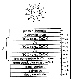
[0015] FIGURE 1 is a cross sectional view of an example photovoltaic device
according to an example embodiment of this invention.
[0016] FIGURE 2 is a refractive index (n) versus wavelength (nm) graph
illustrating refractive indices (n) of glass, a TCO film, silver thin film,
and
hydrogenated silicon (in amorphous, micro- or poly-crystalline phase).
[0017] FIGURE 3 is a percent transmission (T%) versus wavelength (nm)
graph illustrating transmission spectra into a hydrogenated Si thin film of a
photovoltaic device comparing examples of this invention versus a comparative
4
CA 02666687 2009-04-17
WO 2008/063255 PCT/US2007/018361
example (TCO reference); this shows that the examples of this invention
(Examples 1,
2 and 3) have increased transmission in the approximately 450-700 nm
wavelength
range and thus increased photovoltaic module output power, compared to the
comparative example (TCO reference).
[0018] FIGURE 4 is a percent reflection (R %) versus wavelength (nm) graph
illustrating reflection spectra from a hydrogenated Si thin film of a
photovoltaic
device comparing the examples of tliis invention (Examples 1, 2 and 3 referred
to in
Fig. 3) versus a comparative example (TCO reference referred to in Fig. 3);
this
shows that the example embodiment of this invention have increased reflection
in the
IR range, thereby reducing the operating temperature of the photovoltaic
module so as
to increase module output power, compared to the comparative example. Because
the
same Examples 1-3 and comparative example (TCO reference) are being referred
to
in Figs. 3 and 4, the same curve identifiers used in Fig. 3 are also used in
Fig. 4.
[0019] FIGURE 5 is a cross sectional view of the photovoltaic device
according to Example I of this invention.
[0020] FIGURE 6 is a cross sectional view of the photovoltaic device
according to Example 2 of this invention.
100211 FIGURE 7 is a cross sectional view of the photovoltaic device
according to Example 3 of this invention.
[0022] FIGURE 8 is a cross sectional view of the photovoltaic device
according to another example embodiment of this invention.
DETAILED DESCRIPTION OF EXAMPLE EMBODIMENTS OF THE
INVENTION
[0023] Referring now more particularly to the figures in which like reference
numerals refer to like parts/layers in the several views.
[0024] Photovoltaic devices such as solar cells convert solar radiation into
usable electrical energy. The energy conversion occurs typically as the result
of the
photovoltaic effect. Solar radiation (e.g., sunlight) -impinging on a
photovoltaic
device and absorbed by an active region of semiconductor material (e.g., a
CA 02666687 2009-04-17
WO 2008/063255 PCT/US2007/018361
semiconductor film including one or more semiconductor layers such as a-Si
layers,
the semiconductor sometimes being called an absorbing layer or film) generates
electron-hole pairs in the active region. The electrons and holes may be
separated by
an electric field of a junction in the photovoltaic device. The separation of
the
electrons and holes by the junction results in the generation of an electric
current and
voltage. In certain example embodiments, the electrons flow toward the region
of the
semiconductor material having n-type conductivity, and holes flow toward the
region
of the semiconductor having p-type conductivity. Current can flow through an
external circuit connecting the n-type region to the p-type region as light
continues to
generate electron-hole pairs in the photovoltaic device.
[0025] In certain example embodiments, single junction amorphous silicon (a-
Si) photovoltaic devices include three semiconductor layers. In particular, a
p-layer,
an n-layer and an i-layer which is intrinsic. The amorphous silicon film
(which may
include one or more layers such as p, n and i type layers) may be of
hydrogenated
amorphous silicon in certain instances, but may also be of or include
hydrogenated
amorphous silicon carbon or hydrogenated amorphous silicon germanium, or the
like,
in certain example embodiments of this invention. For example and without
limitation, when a photon of light is absorbed in the i-layer it gives rise to
a unit of
electrical current (an electron-hole pair). The p and n-layers, which contain
charged
dopant ions, set up an electric field across the i-layer which draws the
electric charge
out of the i-layer and sends it to an optional external circuit where it can
provide
power for electrical components. It is noted that while certain example
embodiments
of this invention are directed toward amorphous-silicon based photovoltaic
devices,
this invention is not so limited and may be used in conjunction with other
types of
photovoltaic devices in certain instances including but not limited to devices
including other types of semiconductor material, single or tandem thin-film
solar
cells, CdS and/or CdTe photovoltaic devices, polysilicon and/or
microcrystalline Si
photovoltaic devices, and the like.
[0026] Fig. I is a cross sectional view of a photovoltaic device according to
an
example embodiment of this invention. The photovoltaic device includes
transparent
front glass substrate 1, optional dielectric layer(s) 2, multilayer front
electrode 3,
6
CA 02666687 2009-04-17
WO 2008/063255 PCT/US2007/018361
active semiconductor film 5 of or including one or more semiconductor layers
(such
as pin, pn, pinpin tandem layer stacks, or the like), back electrode/contact 7
which
may be of a TCO or a metal, an optional encapsulant 9 or adhesive of a
material such
as ethyl vinyl acetate (EVA) or the like, and an optional superstrate 11 of a
material
such as glass. Of course, other layer(s) which are not shown may also be
provided in
the device. Front glass substrate 1 and/or rear superstrate (substrate) 11 may
be made
of soda-lime-silica based glass in certain example embodiments of this
invention; and
it may have low iron content and/or an antireflection coating thereon to
optimize
transmission in certain example instances. While substrates 1, 11 may be of
glass in
certain example embodiments of this invention, other materials such as quartz
or the
like may instead be used for substrate(s) I and/or 11. Moreover, superstrate
11 is
optional in certain instances. Glass I and/or 11 may or may not be thermally
tempered and/or patterned in certain example embodiments of this invention.
Additionally, it will be appreciated that the word "on" as used herein covers
both a
layer being directly on and indirectly on something, with other layers
possibly being
located therebetween.
[0027] Dielectric layer 2 may be of any substantially transparent material
such
as a metal oxide and/or nitride which has a refractive index of from about 1.5
to 2.5,
more preferably from about 1.6 to 2.5, more preferably from about 1.6 to 2.2,
more
preferably from about 1.6 to 2.0, and most preferably from about 1.6 to 1.8.
However, in certain situations, the dielectric layer 2 may have a refractive
index (n) of
from about 2.3 to 2.5. Example materials for dielectric layer 2 include
silicon oxide,
silicon nitride, silicon oxynitride, zinc oxide, tin oxide, titanium oxide
(e.g., Ti02),
aluminum oxynitride, aluminum oxide, or mixtures thereof. Dielectric layer 2
functions as a barrier layer in certain example embodiments of this invention,
to
reduce materials such as sodium from migrating outwardly from the glass
substrate 1
and reaching the IR reflecting layer(s) and/or semiconductor. Moreover,
dielectric
layer 2 is material having a refractive index (n) in the range discussed
above, in order
to reduce visible light reflection and thus increase transmission of visible
light (e.g.,
light from about 450-700 nm and/or 450-600 nm) through the coating and into
the
semiconductor 5 which leads to increased photovoltaic module output power.
7
CA 02666687 2009-04-17
WO 2008/063255 PCT/US2007/018361
[0028] Still referring to Fig. 1, multilayer front electrode 3 in the.example
embodiment shown in Fig. 1, which is provided for purposes of example only and
is
not intended to be limiting, includes from the glass substrate 1 outwardly
first
transparent conductive oxide (TCO) or dielectric layer 3a, first conductive
substantially metallic IR reflecting layer 3b, second TCO or dielectric layer
3c,
second conductive substantially metallic IR reflecting layer 3d, third TCO or
dielectric layer 33, and optional buffer layer 3f. Optionally, layer 3a may be
a
dielectric layer instead of a TCO in certain example instances and serve as a
seed
layer for the layer 3b. This multilayer film 3 makes up the front electrode in
certain
example embodiments of this invention. Of course, it is possible for certain
layers of
electrode 3 to be removed in certain alternative embodiments of this invention
(e.g.,
one or more of layers 3a, 3c, 3d and/or 3e may be removed), and it is also
possible for
additional layers to be provided in the multilayer electrode 3. Front
electrode 3 may
be continuous across all or a substantial portion of glass substrate 1, or
altematively
maybe patterned into a desired design (e.g., stripes), in different example
embodiments of this invention. Each of layers/films 1-3 is substantially
transparent in
certain example embodiments of this invention.
[0029] First and second conductive substantially metallic- IR reflecting
layers
3b and 3d may be of or based on any suitable IR reflecting material such as
silver,
gold, or the like. These materials reflect significant amounts of IR
radiation, thereby
reducing the amount of IR which reaches the semiconductor film 5. Since IR
increases the-temperature of the device, the reduction of the amount of IR
radiation
reaching the semiconductor film 5 is advantageous in that it reduces the
operating
temperature of the photovoltaic module so as to increase module output power.
Moreover, the highly conductive nature of these substantially metallic layers
3b
and/or 3d permits the conductivity of the overall electrode 3 to be increased.
In
certain example embodiments of this invention, the multilayer electrode 3 has
a sheet
resistance of less than or equal to about 12 ohms/square, more preferably less
than or
equal to about 9 ohms/square, and even more preferably less than or equal to
about 6
ohms/square. Again, the increased conductivity (same as reduced sheet
resistance)
increases the overall photovoltaic module output power, by reducing resistive
losses
in the lateral direction in which current flows to be collected at the edge of
cell
8
CA 02666687 2009-04-17
WO 2008/063255 PCT/US2007/018361
segments. It is noted that first and second conductive substantially metallic
IR
reflecting layers 3b and 3d (as well as the other layers of the electrode 3)
are thin
enough so as to be substantially transparent to visible light. In certain
example
embodiments of this invention, first and/or second conductive substantially
metallic
IR reflecting layers 3b and/or 3d are each from about 3 to 12 nm thick, more
preferably from about 5 to 10 nm thick, and most preferably from about 5 to 8
nm
thick. In embodiments where one of the layers 3b or 3d is not used, then the
remaining conductive substantially metallic IR reflecting layer may be from
about 3
to 18 nrn thick, more preferably from about 5 to 12 nm thick, and most
preferably
from about 6 to 11 nm thick in certain example embodiments of this invention.
These
thicknesses are desirable in that they permit the layers 3b and/or 3d to
reflect
significant amounts of IR radiation, while at the same time being
substantially
transparent to visible radiation which is permitted to reach the semiconductor
5 to be
transformed by the photovoltaic device into electrical energy. The highly
conductive
IR reflecting layers 3b and 3d attribute to the overall conductivity of the
electrode 3
much more than the TCO layers; this allows for expansion of the process
window(s)
of the TCO layer(s) which has a limited window area to achieve both high
conductivity and transparency.
[0030] First, second, and third TCO layers 3a, 3c and 3e, respectively, may be
of any suitable TCO material including but not limited to conducive forms of
zinc
oxide, zinc aluminum oxide, tin oxide, indium-tin-oxide, indium zinc oxide
(which
may or may not be doped with silver), or the like. These layers are typically
substoichiometric so as to render them conductive as is known in the art. For
example, these layers are made of material(s) which gives them a sheet
resistance of
no more than about 30 ohms/square (more preferably no more than about 25, and
most preferably no more than about 20 ohms/square) when at a non-limiting
reference
thickness of about 400 nm. One or more of these layers may be doped with other
materials such as nitrogen, fluorine, aluminum or the like in certain example
instances, so long as they remain conductive and substantially transparent to
visible
light. In certain example embodiments of this invention, TCO layers 3c and/or
3e are
thicker than layer 3a (e.g., at least about 5 nm, more preferably at least
about 10, and
most preferably at least about 20 or 30 nm thicker). In certain example
embodiments
9
CA 02666687 2009-04-17
WO 2008/063255 PCT/US2007/018361
of this invention, TCO layer 3a is from about 3 to 80 nm thick, more
preferably from
about 5-30 nm thick, with an example thickness being about 10 nm.
Optionallayer 3a
is provided mainly as a seeding layer for layer 3b and/or for antireflection
purposes,
and its conductivity is not as important as that of layers 3b-3e (thus, layer
3a may.be a
dielectric instead of a TCO in certain example embodiments). In certain
example
embodiments of this invention, TCO layer 3c is from about 20 to 150 nm thick,
more
preferably from about 40 to 120 nm thick, with an example thickness being
about 74-
75 nm. In certain example embodiments of this invention, TCO layer 3e is from
about 20 to 180 nm thick, more preferably from about 40 to 130 nm thick, with
an
example thickness being about 94 or 115 nm. In certain example embodiments,
part
of layer 3e, e.g., from about 1-25 nm or 5-25 nm thick portion, at the
interface
between layers 3e and 5 may be replaced with a low conductivity high
refractive
index (n) film 3f such as titanium oxide to enhance transmission of light as
well as to
reduce back diffusion of generated electrical carriers; in this way
performance may be
further improved. It is noted that one or more of layers 3a, 3c and/or 3e may
be
dielectric instead of TCO in certain alternative example embodiments of this
invention. Accordingly, all layers of the front electrode 3 need not be
conductive,
since some of the layer(s) of the front electrode 3 may be dielectric in
certain example
embodiments of this invention.
[0031] In certain example embodiments of this invention, the photovoltaic
device may be made by providing glass substrate 1, and then depositing (e.g.,
via
sputtering or any other suitable technique) multilayer electrode 3 on the
substrate 1.
Thereafter the structure including substrate I and front electrode 3 is
coupled with the
rest of the device in order to form the photovoltaic device shown in Fig. 1.
For
example, the semiconductor layer 5 may then be formed over the front electrode
on
substrate 1. Alternatively, the back contact 7 and semiconductor 5 may be
fabricated/formed on substrate I 1(e.g., of glass or other suitable material)
first; then
the electrode 3 and dielectric 2 may be formed on semiconductor 5 and
encapsulated
by the substrate 1 via an adhesive such as EVA.
[0032] The alternating nature of the TCO layers 3a, 3c and/or 3e, and the
conductive substantially metallic IR reflecting layers 3b and/or 3d, is also
CA 02666687 2009-04-17
WO 2008/063255 PCT/US2007/018361
advantageous in that it also one, two, three, four or all of the following
advantages to
be realized: (a) reduced sheet resistance (RS) of the overall electrode 3 and
thus
increased conductivity and improved overall photovoltaic module output power;
(b)
increased reflection of infrared (IR) radiation by the electrode 3 thereby
reducing the
operating temperature of the semiconductor 5 portion of the photovoltaic
module so
as to increase inodule output power; (c) reduced reflection and increased
transrriission
of light in the visible region of from about 450-700 nm (and/or 450-600 nm) by
the
front electrode 3 which leads to increased photovoltaic module output power;
(d)
reduced total thickness of the front electrode coating 3 which can reduce
fabrication
costs and/or time; and/or (e) an improved or enlarged process window in
forming the
TCO layer(s) because of the reduced impact of the TCO's conductivity on the
overall
electric properties of the module given the presence of the highly conductive
substantially metallic layer(s).
[0033] The active semiconductor region or film 5 may include one or more
layers, and may be of any suitable material. For example, the active
semiconductor
film 5 of one type of single junction amorphous silicon (a-Si) photovoltaic
device
includes three semiconductor layers, namely a p-layer, an n-layer and an i-
layer. The
p-type a-Si layer of the semiconductor film 5 may be the uppermost portion of
the
semiconductor film 5 in certain example embodiments of this invention; and the
i-
layer is typically located between the p and n-type layers. These amorphous
silicon
based layers of film 5 may be of hydrogenated amorphous silicon in certain
instances,
but may also be of or include hydrogenated amorphous silicon carbon or
hydrogenated amorphous silicon germanium, hydrogenated microcrystalline
silicon,
or other suitable material(s) in certain example embodiments of this
invention. It is
possible for the active region 5 to be of a double-junction or triple-junction
type in
alternative embodiments of this invention. CdTe and/or CdS may also be used
for
semiconductor film 5 in alternative embodiments of this invention.
100341 Back contact, reflector and/or electrode 7 may be of any suitable
electrically conductive material. For example and without limitation, the back
contact
or electrode 7 may be of a TCO and/or a metal in certain instances. Example
TCO
materials for use as back contact or electrode 7 include indium zinc oxide,
indium-tin-
11
CA 02666687 2009-04-17
WO 2008/063255 PCT/US2007/018361
oxide (ITO), tin oxide, and/or zinc oxide which may be doped with aluminum
(which
may or may not be doped with silver). The TCO of the back contact 7 may be of
the
single layer type or a multi-layer type in different instances. Moreover, the
back
contact 7 may include both a TCO portion and a metal portion in certain
instances.
For example, in an example multi-layer embodiment, the TCO portion of the back
contact 7 may include a layer of a material such as indium zinc oxide (which
may or
may not be doped with silver), indium-tin-oxide (ITO), tin oxide, and/or zinc
oxide
closest to the active region 5, and the back contact may include another
conductive
and possibly reflective layer of a material such as silver, molybdenum,
platinum,
steel, iron, niobium, titanium, chromium, bismuth, antimony, or aluminum
further
from the active region 5 and closer to the superstrate 11. The metal portion
may be
closer to superstrate 11 compared to the TCO portion of the back contact 7.
[0035) The photovoltaic module may be encapsulated or partially covered
with an encapsulating material such as encapsulant 9 in certain example
embodiments. An example encapsulant or adhesive for layer 9 is EVA or PVB.
However, other materials such as Tedlar type plastic, Nuvasil type plastic,
Tefzel type
plastic or the like may instead be used for layer 9 in different instances.
[0036] Utilizing the highly conductive substantially metallic IR reflecting
layers 3b and 3d, and TCO layers 3a, 3c and 3d, to form a multilayer front
electrode
3, permits the thin film photovoltaic device performance to be improved by
reduced
sheet resistance (increased conductivity) and tailored reflection and
transmission
spectra which best fit photovoltaic device response. Refractive indices of
glass 1,
hydrogenated a-Si as an example semiconductor 5, Ag as an example for layers
3b
and 3d, and an example TCO are shown in Fig. 2. Based on these refractive
indices
(n), predicted transmission spectra impinging into the semiconductor 5 from
the
incident surface of substrate I are shown in Fig. 3. In particular, Fig. 3 is
a percent
transmission (T%) versus wavelength (nm) graph illustrating transmission
spectra into
a hydrogenated Si thin film 5 of a photovoltaic device comparing Examples 1-3
of
this invention (see Examples 1-3 in Figs. 5-7) versus a comparative example
(TCO
reference). The TCO reference was made up of 3 mm thick glass substrate I and
from the glass outwardly 30 nm of tin oxide, 20 nm of silicon oxide and 350 nm
of
12
CA 02666687 2009-04-17
WO 2008/063255 PCT/US2007/018361
TCO. Fig. 3 thus shows that the examples of this invention (Examples 1-3 shown
in
Figs. 5-7) has increased transmission in the approximately 450-600 and 450-700
nm
wavelength ranges and thus increased photovoltaic module output power,
compared
to the comparative example (TCO reference).
[00371 Example 1 shown in Fig. 5 and charted in Figs. 3-4 was made up of 3
mm thick glass substrate 1, 16nm thick TiO2 dielectric layer 2, 10 nm thick
zinc_oxide
TCO doped with A] 3a, 8 nm thick Ag IR reflecting layer 3b, and 115 nm thick
zinc
oxide TCO doped with Al 3e. Layers 3c, 3d and 3f were not present in Example
1.
Example 2 shown in Fig. 6 and charted in Figs. 3-4 was made up of 3 mm thick
glass
substrate 1, 16nm thick Ti02 dielectric layer 2, 10 nm thick zinc oxide TCO
doped
with Al 3a, 8 mn thick Ag IR reflecting layer 3b, 100 nm thick zinc oxide TCO
doped
with A] 3e, and 20 nm thick titanium suboxide layer 3f. Example 3 shown in
Fig. 7
and charted in Figs. 3-4 was made up of 3 mm thick glass substrate 1, 45 nm
thick
dielectric layer 2, 10 nm thick zinc oxide TCO doped with Al 3a, 5 nrn thick
Ag IR
reflecting layer 3b, 75 nm thick zinc oxide TCO doped with Al 3c, 7 nm thick
Ag IR
reflecting layer 3d, 95 nm thick zinc oxide TCO doped with Al 3e, and 20 nm
thick
titanium suboxide layer 3f. These single and double-silver layered coatings of
Examples 1-3 had a sheet resistance less than 10 ohms/square and 6
ohms/square,
respectively, and total thicknesses much less than the 400 nm thickness of the
prior
art. Examples 1-3 had tailored transmission spectra, as shown in Fig. 3,
having more
than 80% transmission into the semiconductor 5 in part or all of the
wavelength range
of from about 450-600 nm and/or 450-700 nm, where AM1.5 has the strongest
intensity.
[00381 Meanwhile, Fig. 4 is a percent reflection (R %) versus wavelength
(nm) graph illustrating reflection spectra from a hydrogenated Si thin film of
a
photovoltaic device comparing Examples 1-3 versus the above mentioned
comparative example; this shows that Exarnples 1-3 had increased reflection in
the IR
range thereby reducing the operating temperature of the photovoltaic modules
so as to
increase module output power, compared to the comparative example. In Fig. 4,
the
low reflection in the visible range of from about 450-600 nm and/or 450-700 nm
(the
cell's high efficiency range) is advantageously coupled with high reflection
in the
13
CA 02666687 2009-04-17
WO 2008/063255 PCT/US2007/018361
near and short IR range beyond about 1000 nm; the high reflection in the near
and
short IR range reduces the absorption of solar thermal energy that will result
in a
better cell output due to the reduced cell temperature and series resistance
in the
module. As shown in Fig. 4, the front glass substrate 1 and front electrode 3
taken
together have a reflectance of at least about 45% (more preferably at least
about 55%)
in a substantial part or majority of a near to short IR wavelength range of
from about
1000-2500 nm and/or 1000 to 2300 nm. In certain example embodiments, it
refelects
at least 50% of solar energy in the range of from 1000-2500 nm and/or 1200-
2300
nm. In certain example embodiments, the front glass substrate and front
electrode 3
taken together have an IR reflectance of at least about 45% and/or 55% in a
substantial part or a majority of an IR wavelength range of from about 1000-
2500 nm,
possibly from 1200-2300 nm. In certain example embodiments, it may block at
least
50% of solar energy in the range of 1000-2500 nm.
[0039] While the electrode 3 is used as a front electrode in a photovoltaic
device in certain embodiments of this invention described and illustrated
herein, it is
also possible to use the electrode 3 as another electrode in the context of a
photovoltaic device or otherwise.
100401 Fig. 8 is a cross sectional view of a photovoltaic device according to
another exampl,e embodiment of this invention. An optional antireflective (AR)
film
may be provided on the incident side of the glass substrate I in any
enibodiment of
this invention, as indicated for example by AR film 1 a' shown in Fig. 8. The
photovoltaic device in Fig. 8 includes glass substrate 1, dielectric layer 2
(e.g., of or
including silicon oxide, silicon oxynitride, silicon nitride, or the like)
which may
function as a sodium barrier for blocking sodium from migrating out of the
glass
substrate 1, AR transition layer 4a (e.g., of or including a dielectric such
as titanium
oxide, niobium oxide, or the like) which in preferred example embodiments may
have
a refractive index (n) of from about 2.2 to 2.6 (more preferably n is from
about 2.3 to
2.5) that is provided for AR purposes in order to decrease reflections off of
the device,
seed layer 4b (e.g., of or including zinc oxide, zinc aluminum oxide, tin
oxide, tin
antimony oxide, indium zinc oxide, or the like) which may be a TCO or
dielectric in
different example embodiments, silver based IR reflecting layer 4c, optional
overcoat
14
CA 02666687 2009-04-17
WO 2008/063255 PCT/US2007/018361
or contact layer 4d (e.g., of or including an oxide of Ni and/or Cr, zinc
oxide, zinc
aluminum oxide, or the like) which may be a TCO or dielectric, TCO 4e (e.g.,
of or
including zinc oxide, zinc aluminum oxide, tin oxide, tin antimony oxide, zinc
tin
oxide, indium tin oxide, indium zinc oxide, or the like), optional buffer
layer 4f (e.g.,
of or including zinc oxide, zinc aluminum oxide, tin oxide, tin antimony
oxide, zinc
tin oxide, indium tin oxide, indium zinc oxide, or the like) which may be
conductive
to some extent, semiconductor 5 (e.g., CdS/CdTe, a-Si, or the like), optional
back
contact, reflector and/or electrode 7, optional adhesive 9, and optional back
glass
substrate 11. It is noted that in certain example embodiments, layer 4b may be
the
same as layer 3a described above, layer 4c may be the same as layer 3b or 3d
described above, layer 4e may be the same as layer 3e described above, and
layer 4f
may be the same as layer 3f described above (see descriptions above as to
other
embodiments in this respect). Likewise, layers 5, 7, 9 and 11 are also
discussed above
in connection with other embodiments.
[0041] For purposes of example only, an example of the Fig. 8 embodiment is
as follows (note that certain optional layers shown in Fig. 8 are not used in
this
example). For example, referring to Fig. 8, glass substrate 1(e.g., about 3.2
mm
thick), dielectric layer 2 (e.g., silicon oxynitride about 20 nm thick), AR
transition
layer 4a (e.g., dielectric TiOx about 20 nm thick), Ag seed layer 4b (e.g.,
dielectric or
TCO zinc oxide or zinc aluminum oxide about 10 nm thick), IR reflecting Iayer
4c
(silver about 5-8 nm thick), TCO 4e (e.g., conductive zinc oxide or zinc
aluminum
oxide about 10 nm thick), and possibly conductive buffer layer 4f (TCO zinc
oxide,
tin oxide, zinc aluminum oxide, ITO, or the like from about 50-250 nm thick,
more
preferably from about 100-150 run thick). In certain example embodiments, the
buffer layer 4f (or 3f) is designed to have a refractive index (n) of from
about 2.1 to
2.4, more preferably from about 2.15 to 2.35, for substantial index matching
to the
semiconductor 5 (e.g., CdS or the like) in order tb improve efficiency of the
device.
100421 The photovoltaic device of Fig. 8 may have a sheet resistance of no
greater than about 18 ohms/square, more preferably no grater than about 15
ohms/square, even more preferably no greater than about 13 ohms/square in
certain
example embodiments of this invention. Moreover, the Fig. 8 embodiment may
have
CA 02666687 2009-04-17
WO 2008/063255 PCT/US2007/018361
tailored transmission spectra having more than 80% transmission into the
semiconductor 5 in part or all of the wavelength range of from about 450-600
nm
and/or 450-700 nm, where AMl.5 may have the strongest intensity.
[0043] While the invention has been described in connection with what is
presently considered to be the most practical and preferred embodiment, it is
to be
understood that the invention is not to be limited to the disclosed
embodiment, but on
the contrary, is intended to cover various modifications and equivalent
arrangements
included within the spirit and scope of the appended claims.
16