Note: Descriptions are shown in the official language in which they were submitted.
CA 02666872 2009-04-17
WO 2008/115205 PCT/US2007/020774
SYSTEM AND METHOD FOR OBJECT ORIENTED HARDWARE
1. FIELD OF THE INVENTION
The present invention relates generally to systems and methods for object-
oriented
hardware.
II. BACKGROUND OF THE INVENTION
A complicated task is usually tackled by breaking it down into smaller tasks.
In
software this is referred to as object oriented design. Objects are defined as
self
contained modules of functionality.
Today's approach to digital product design (such as, e.g., the design of
digital
televisions) is focused on maximizing integration with the ideal of a system
on a chip.
As recognized herein, this hardware complexity results in a long lead time
which may
sacrifice flexibility for unit cost savings. By the time a chip is ready, it
may lack some
desired features and yet include unused capabilities. Additional parts thus
may be
required achieve the desired feature set while at the same time building up
the amount of
obsolete or at least no longer desired capabilities of the chip. Software is
then given the
task of making all the components work together.
As further recognized herein, a digital product need not always require a
general
purpose computer. Moreover, timesharing generic busses may not be the best way
to
move dedicated data.
1
CA 02666872 2009-04-17
WO 2008/115205 PCT/US2007/020774
As still further recognized herein, most consumer electronics have a specific
task
to perform and any changes to the task are paced by slow human input. Task
breakdown
usually entails a series of steps or functions that are performed as a serial
pipeline, with
specific products varying by details of specific functions and the performance
order.
Thus, such CE products including digital televisions are, as understood
herein, candidates
for object-oriented hardware architecture.
SUMMARY OF THE INVENTION
An object-oriented hardware system includes one or more hardware-implemented
signal processing modules each configured to execute a single function and one
or more
input and/or output modules configured to send data to or receive data from
the signal
processing module. The signal processing module is more than a single
electronic
component and is less than an entire separately-vended CE device.
For example, the signal processing module can be a filter module, a decryption
module, an encryption module, a transcode module, a multiplexer module, a
demultiplexer module, a scaler module, or a high definition media interface
(HDMI)
receiver module. In contrast, the input and/or output module can be a first in
first out
(FIFO) buffer module, a P_O_D_ ("POD") module, a removable memory
medium, a video delivery module, an iLink interface module, a personal
computer
interface (PCI) interface module, and an integrated drive electronics (IDE)
interface. A
universal pipeline switch may be used to connect the modules to, e.g., an
image
2
CA 02666872 2009-04-17
WO 2008/115205 PCT/US2007/020774
compositer module, or an image mirror module, with video information from the
HDMI
receiver being sent to a display driver module for display of video on a
visual display.
In another aspect, a method for architecting a consumer electronic (CE) device
includes establishing plural object-oriented hardware modules with common
communication capabilities. The method also includes selecting a subset of the
modules
and configuring the subset of modules in a design to achieve the CE device.
In yet another aspect, an object-oriented hardware system includes one or more
hardware-implemented signal processing modules and one or more input and/or
output
modules configured to send data to or receive data from the signal processing
module.
The signal processing module is more than a single electronic component and is
less than
an entire separately-vended CE device.
The details of the present invention, both as to its structure and operation,
can best
be understood in reference to the accompanying drawings, in which like
reference
numerals refer to like parts, and in which:
BRIEF DESCRIPTION OF THE DRAWINGS
Figure 1 is a block diagram of a first example object-oriented hardware
system;
Figure 2 is a block diagram of a second example object-oriented hardware
system;
and
Figure 3 is a block diagram of an example module (a scaler) that can be used
in an
object-oriented hardware system.
3
CA 02666872 2009-04-17
WO 2008/115205 PCT/US2007/020774
DETAILED DESCRIPTION OF THE PREFERRED EMBODIMENT
In general overview, the present invention recognizes that the architecture
for a
CE product can be designed using a library of hardware objects connected
together using
a common interface structure. As understood herein, this hardware modularity
maximizes product feature flexibility and permits commoditization at the
module level
rather than at the product level. Object-oriented hardware architecture
implicates three
issues addressed below: objects, interfaces, and data routing.
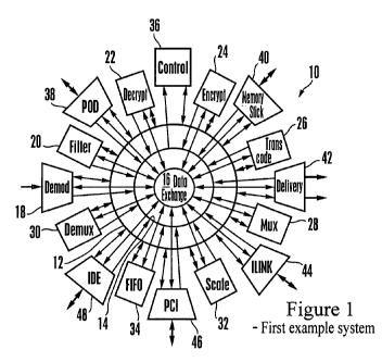
Referring initially to Figure 1, a first non-limiting object-oriented hardware
system is shown, generally designated 10, in which various hardware-
implemented
modules (also referred to herein as "objects") follow desired functions. That
is, any
function performed in a system is a candidate as a hardware module. This
breakdown
permits easy use and substitution of function as needed.
By "hardware module" or "hardware object" is meant more than a single
electronic component such as a single resistor, capacitor, or transistor and
less than an
entire separately-vended CE component such as an entire TV, disk player, PVR,
etc.
Among the hardware objects that are contemplated herein are NTSC tuners,
ATSC tuners, analog input modules for composite, S-Video, and component input,
an IP
network communication module, a HDMI (or DVI) input module, a VGA input
module,
a decoder (MPEG, AVC, DV, etc.) module, a scaler module, an image enhancement
module (e.g., a de-interlace module), a graphics generator module for
generating user
interfaces, and a display driver module.
4
CA 02666872 2009-04-17
WO 2008/115205 PCT/US2007/020774
Accordingly, it may be appreciated that an object oriented hardware approach
establishes a library of modules that can be pipelined together or switched
in/out of the
data path to achieve the desired functionality.
Figure 1 shows a first example system 10 using present object-oriented
hardware
principles that may be employed as a video processing system for a TV. Each of
the
elements shown in Figure 1 may be implemented by a respective hardware module,
and
all the hardware modules may be located on the same substrate if desired. The
modules
communicate by means of three switches 12, 14, 16 to effect data exchange. The
switches 12, 14, 16 may be cross point switches that permit any input to be
routed to any
output, as more fully disclosed below.
Among the modules shown in the non-limiting example of Figure 1 are a
demodulator module 18 that receives information from, e.g., an audio-video
source. A
filter module 20 may be provided to filter the signal and a decryption module
22 may
likewise be provided to decrypt an encrypted data stream. Likewise, an
encryption
module 24 may be provided to encrypt data that is output by the system 10.
Transcoding
of video can be undertaken by a transcode module 26.
Multiplexing of outgoing data and demultiplexing of incoming data can be
provided.by a multiplexer module 28 and a demultiplexer module 30,
respectively.
Video scaling may be provided by a scaler module 32, and data input and/or
output
handled by a first in first out (FIFO) buffer module 34. A control module 36
that may be
implemented by a field programmable gate array (FPGA) may control/coordinate
various
activities of the above signal processing modules.
CA 02666872 2009-04-17
WO 2008/115205 PCT/US2007/020774
In addition to the above signal processing modules each of which in general is
configured to execute one and only one function, Figure 1 shows that the
system 10 may
also include various input/output modules for communicating with components
external
to the system 10. By way of non-limiting example, the system 10 may include a
P_O_D_ ("POD") module 38, a removable memory medium 40 such as a Sony
Memory Stick (which is a trademark of Sony Corp.), a video delivery module 42,
an
iLink interface module 44, a personal computer interface (PCI) interface
module 46, and
an integrated drive electronics (IDE) interface 48.
Figure 2 shows another example object-oriented hardware module system 50 that
can be used to drive a TV display. As shown, the system 10 can receive video
information from first through third source interface modules 52, 54, 56, each
of which
can send video stream protected by digital rights management to a respective
high
definition media interface (HDMI) receiver module 58, 60, 62. The streams from
the
HDMI receiver modules can be switched through a universal pipeline switch 64
to
appropriate signal processing modules such as an image compositer module 66
(for, e.g.,
rendering a composite image from the three data streams) and an image mirror
module
68. Outputs of the signal processing modules can be sent through the switch 64
as shown
to a display driver 70 for presenting video images on a TV display 72.
A more detailed example of a module used in a digital TV can be seen in Figure
3, which illustrates a scaler module. The illustrated scaler module receives
frames of
video at an input FIFO 74, demultiplexes it at a demultiplexer 76, and then
processes it
through an input canvas 78, clipper 80, and scaler processor 82 to resize the
video to meet
6
CA 02666872 2009-04-17
WO 2008/115205 PCT/US2007/020774
needs of subsequent modules. The resized video is sent through an output
canvas 84 and
output to subsequent modules through an output FIFO buffer 86. Control
parameters can
describe the input format and the desired output format. Microcode can be
loaded or
selected if there are options for the scaler algorithm.
As understood by the present invention, the above-described hardware
modularity
is most versatile when a common interface is used to interconnect modules.
While
specialized modules interface to outside components, internal interconnections
are
interchangeable because of the shared interface.
An important interface carries the pipelined data from module to module.
Serial
multi-gigabit technologies such as those used for PCI express and gigabit
Ethernet can be
used. These communication methods transfer data over a simple pair of wires
traversing
tens of centimeters, easily accommodating distribution within, e.g., a TV
chassis. Data
rates for each module in a pipeline can be common to the system or
be.programmed to
match the fixed or dynamic needs of each point-to-point connection. Digital
rights
management support may also be included to protect data.
Other components of a common interface can include a means to exchange
control and status information. This could be serviced by 12C or similar low
bit rate bus
to avoid royalty issues. A common reference clock source can be distributed to
all
modules. An internal phase-locked loop (PLL) or similar clock multiplier could
use, e.g.,
25MHz to generate the required internal clocks. A low speed metronome-like
strobe (i.e.,
a frame clock) can be used for system synchronization.
7
CA 02666872 2009-04-17
WO 2008/115205 PCT/US2007/020774
Turning now to data routing, dedicated simple connections can exist between
modules that always feed each other, but as mentioned above greater
flexibility can be
achieved by using switches. These can also facilitate clustering modules in
different
areas on the chassis. Switches can range from low tech selectors to much more
versatile
cross points.
A cross point switch permits any input to be routed to any output (even more
than
one output simultaneously). Dynamic configuration can be used to change
modules in
and out of the logical pipeline. Even the sequence order can be changed. FIFOs
can be
implemented at the junction points to smooth out data and match clock rates.
In addition to the above description, as contemplated herein the object-
oriented
hardware modules of the present invention can be unit tested then verified as
an addition
to a known working system. New modules can be phased into active production
lines.
The most versatile form of integration is to connect each module to a single
cross point.
Or, modules may be combined into sub-systems that appear as a single module
with a superset of capability. An example might be for an analog input
interface that
could be used across multiple products. Common packaging for modules that
frequently
are used in the same product can result in cost savings. Other modules can be
configured
as physical plug-ins that encourage field upgrades.
For system setup and control a simple microprocessor or a state machine may be
used, as mentioned above in relation to Figure 1. Control can include object
initialization
and data routing specification.
8
CA 02666872 2009-04-17
WO 2008/115205 PCT/US2007/020774
Operation of a module pipeline can start with selection of an operational
mode.
This will cause any necessary microcode to be loaded (via the pipeline bus)
and switches
to be set matching the desired topology. Specifics can be described in a table
to make
mode changes easy.
With the above disclosure in mind, it may now be appreciated that object
oriented
hardware is an advantageous systems approach to design and build digital
consumer
electronics. It splits the product into separate functional tasks that can be
perfected in
isolation and be swapped in and out to meet the needs of the customer. It is
very agile
and permits rapid response to changes and demands in the marketplace.
Additional Non-Limiting Implementation Details
Data can be transmitted serially with a sync line asserted when the first bit
of a
serial burst or buffer is sent. The sync signal may be removed immediately
after the first
data bit or any time before the gap time between bursts. Receiving modules may
use the
asserting edge of the sync signal to indicate the start of a new buffer. The
format of a
buffer can be anything agreed to by both the sending and receiving modules. A
typical
format might be that of a serial MPEG2 transport stream.
"Push" mode may be implemented by having the sending module drive the clock
line. "Pull" mode can be implemented by having the receive module drive the
clock line.
An optional ready line can be driven by the side not driving the clock for
flow control. A
fifth line can be used to flag buffers with errors but generally transmission
and content
errors can be handled with "in band" bits or by using the control/notification
busses.
9
CA 02666872 2009-04-17
WO 2008/115205 PCT/US2007/020774
Push/pull mode can be a configuration register option for all serial data
stream
connections.
Each serial port connection can be configurable as to direction and stream
type.
Four or five pins may be used for each port. The primary four signals may be
used for
serial transport streams and the fifth provides a mechanism for the external
device to
provide a stream address.
* Serial data (input/output)
* Data clock (input/output)
* Data sync (input/output- same as data)
* Valid/ready (not valid asserted by source, not ready asserted by receiver)
* Address (input indicates stream being transferred)
The cross point switch mentioned above can have addressable ports when the
clock is supplied externally. This means an additional input line that
provides the cross
point with an asynchronous address value to further specify the port address.
The port
subaddress may be supplied by first asserting a start bit and then a four bit
address value
and check bit for a total of six bits. Bit transitions can be synchronized by
the system
generic clock value. The sub address may remain in effect until explicitly
replaced by
another sub address. This feature is useful when connecting to devices that
have time
multiplexed streams such as 1394, USB, Ethernet, etc.
The interface used to pass data between modules may be standardized to
facilitate
easy interconnection.
CA 02666872 2009-04-17
WO 2008/115205 PCT/US2007/020774
In addition to a connection to the control bus, modules can have input data
streams, output data streams, a connection to the notification bus, and even a
connection
to an outside bus or device.
Inter-module communication summary
Communication between the modules can use three common mechanisms -
control, notification, and data. All three can be serial implementations to
minimize the
number of connections.
Traits that may be common to all modules
* System clock
* Software reset
* Power save mode
Several characteristics may be common to all modules. A system clock is
supplied to all modules to be used for timing purposes. (This clock may be
used for
serial data bus clocking, but it is not required.) A control register can be
used to reset a
module to the same state as power-up. Another register can be used to put the
module
into power save mode. When in power save mode, the module uses the least
amount of
power possible by only being receptive to a command to leave power save mode.
Control/Status Bus
Control can be performed via an 12C bus. This provides access to configuration
registers, command delivery and status retrieval.
Notification Bus
11
CA 02666872 2009-04-17
WO 2008/115205 PCT/US2007/020774
One of the buses above may be a notification bus that can be used for special
completion or contingency type messages typically implemented in an interrupt
structure.
Each module that can produce a notification can have a configuration register
for each
possible use. Notifications may be queued for processing by the control
module(s). Any
type of module can send a notification, but only a control module is expected
to process
it.
Each notification may be 32 bits long and in a format defined by the control
module. (Recall that the control module is responsible for initializing the
configuration
registers in each module.) A value of zero is assumed to be inactive and is
the power up
or reset condition. Bits within the notification may be assigned to indicate
the ID of the
servicing control module, the notification priority and the notification
description.
Notifications may either be self regenerative or require re-arming to be
resent.
Self regenerating notifications may be sent automatically every time an event
happens to
trigger the notification. This would usually apply to aperiodic and unexpected
events.
State sensitive notifications such as buffer starvation may be sent only on
the state change
and not repeatedly sent with each system clock. Re-armed notifications may
require a
command to acknowledge the notification before can be resent.
The notification bus may be a single line with open collector drivers and the
system clock used for edge synchronization. Any module can drive the bus low
at any
time. Before sending a notification, a module listens to the notification bus
for sixteen
clock periods (notification length) to assure that the bus is quiescent. Each
notification
can be initiated by asserting a start bit followed by the data bits MSB first.
As a module
12
CA 02666872 2009-04-17
WO 2008/115205 PCT/US2007/020774
is asserting logical one bits of its notification, it checks to see if another
module is
asserting a logical zero at the same time. If such a collision is detected,
the module
asserting a logical one suspends its assertion and waits for the bus to be
quiescent again.
This collision management scheme causes the lowest value notification to have
the
highest priority and introduces no delay to the higher priority notification.
A special circuit may be used to receive the notifications. It can act as a
prioritizing pre filter for the servicing CPU or other control device.
Notifications can be
queued in FIFO like list in priority order. A level type interrupt can be
asserted whenever
any notifications are queued. Reads of the device (it looks like a location of
memory) can
produce the highest priority (lowest numeric value) pending notification.
Reading an
empty notification can produce a value of "all ones" indicating a null
notification. A
special notification can be self generated by the device if the queue
overflows. (High
order bits a zero, n low order bits indicating the number of discards.)
Examples of modules that can be used include:
* QAM demodulator
* 8VSB demodulator
* Cross point switch
* NTSC to MPEG2 transcoder
* MPEG to NTSC transcoder
* DV to MPEG2 transcoder
* PID filter and translator
* Serial data stream to CPU buffer (via PCI initiator)
* CPU buffer to Serial data stream (via PCI initiator)
* Decryption module
* Encryption module
* Video demultiplexor (output component video)
* Audio demultiplexor (right/left outputs)
* Audio demultiplexor (5.1 outputs)
* Audio demultiplexor(other outputs)
13
CA 02666872 2009-04-17
WO 2008/115205 PCT/US2007/020774
* Generic FPGA (with dynamically downloadable program)
* System controller (CPU with RAM, ROM, flash)
* Data stream FIFO
* Voice over IP
'k Point of Deployment (POD)
'k DAVIC
* DOCSIS
* i.LINK (1394)
* Memory Stick
* IDE
FIFO module
The FIFO modules can be memory elements used to buffer data on a First
In/First
Out basis. They can also be used as a store and forward element, a delay line,
rescan
buffer mode, or even flow control based upon time stamps.
As a FIFO, data can be pushed in (or pulled in when data is available) from
the
upstream element and pulled out by the downstream element. Data bits are
normally
stored individually but a run length encoding scheme could be used for
compressible
data. For stream types with long data blocks, sync bits from the input stream
may be
preserved within the FIFO by counter registers organized as a subFIFO within
the main
FIFO. A counter register can be incremented as data bits are clocked in. When
a sync bit
is encountered, the register can be pushed onto the subFIFO and a new counter
started.
As data bits are pulled out of the FIFO, the oldest counter is decremented
with each bit
until the counter reaches zero. At this point the output sync signal is
asserted and the
next counter pulled from the subFIFO. For short data block stream types, the
sync bits
can be stored as a parallel bit stream to the main data stream.
Store and forward feature may be used to move status information from the end
of
a data buffer to the beginning. Data may be pushed into the FIFO in the normal
manner
14
CA 02666872 2009-04-17
WO 2008/115205 PCT/US2007/020774
but output availability is held off until the entire buffer has been received.
A
programmable counter may be used to specify the length of the buffer. The
final trailing
bits received may be preserved as buffer status and the output side of the
FIFO is enabled.
The status bits can be transmitted (stream location TBD) first before the main
data. This
feature permits a source module (without its own storage) to build a buffer on
the fly and
flag a flaw after the fact. The destination module (also without its own
storage) learns of
the flaw up front.
The FIFO can be used as a delay line by programming a minimum buffer depth.
Data is pushed in as with a normal FIFO but output availability is not
asserted unless the
required amount of data is queued. This eases the job of synchronizing
multiple streams
(i.e. audio lip sync).
Rescan buffer mode permits the same data to be pulled from the buffer
repeatedly
until replaced by a fresh push. This can be used for insertion packets that
are injected
periodically into a stream but are updated only occasionally. Random writes
are
permitted.
Flow control FIFOs can be implemented by prepending a time stamp to the
beginning of each buffer. This time stamp may have been done by an upstream
process
or as part of the FIFO input hardware. Data out of the FIFO can be held up
until the
internal time reference reaches the time stamp value attached to the buffer on
the head of
the queue or the next buffer is discarded if its time stamp is "stale".
CA 02666872 2009-04-17
WO 2008/115205 PCT/US2007/020774
The input ready line can be programmed to range in meaning from actually full
to
a water mark, and the same is true for the output ready line. Read and write
pointers can
be under program control.
PCI support requires one of the more complicated modules. Module features may
include PCI interface configuration registers, memory mapped access to the 12C
control/status bus, and DMA like support for multiple stream transfers.
Eight simultaneous serial data stream transfers can be active at one time.
Each
stream has a double ranked set of address/counter registers and several
operating modes.
The counter specifies the number of bytes to transfer and the address points
to the transfer
location on the PCI memory bus. A stream specific control register specifies
the transfer
direction, if double stacking is active, if the same buffer is to be used as a
continuous
loop, how to report transfer complete, if the transfer is push/pull, etc.
Additionally, a system may include any number of CPU modules. If CPU support
is provided outside the module, there not need be any internal CPU. At the
other end of
the spectrum can be systems with multiple CPU modules. One CPU might handle
security issues such as key handling and generation. Another CPU might turn
front end
modules that tune, FEC, and demodulate a signal into a self standing tuner
subsystem.
The cross point switch referred to above can be used as a generic and flexible
means to exchange data between modules Any input can be routed to any output.
Inputs
can be routed to more than one output simultaneously. Cross point switches can
be
cascaded to form larger switches that can handle more streams.
16
CA 02666872 2009-04-17
WO 2008/115205 PCT/US2007/020774
The cross point ports can be programmed to operate in either push or pull mode
and could even include a small amount of buffering to eliminate the need for a
full FIFO.
Accordingly, modules in accordance with present principles may fall into five
basic categories, namely, control, data exchange, internal processing,
storage, and edge or
external interface. Control modules are responsible for conscious decision
making and
orchestrating the data flow between the processing modules. Data exchange
modules
serve as an autonomous nervous system to keep the data flowing with a minimum
of
control intervention. A combination of physical and logical "plumbing" routes
the data
streams between modules. Processing modules combine, split, and transform data
to
achieve their design function. One or more data streams may be input and one
or more
data streams may be output. Programmed registers control the value added
features.
Storage modules preserve data between processes and are usually implemented as
FIFOs.
Edge pieces interface with the outside world. This might be an electrical
transformation
such as analog to digital.
While the particular SYSTEM AND METHOD FOR OBJECT ORIENTED
HARDWARE is herein shown and described in detail, it is to be understood that
the
subject matter which is encompassed by the present invention is limited only
by the
claims.
17