Note: Descriptions are shown in the official language in which they were submitted.
CA 02667145 2009-04-20
WO 2008/032048 PCT/GB2007/003431
- 1 -
ELECTRO-OPTIC WAVEGUIDE POLARISATION MODULATOR
The present invention relates to an electro-optic waveguide polarisation
modulator and
to a method of operating the same. The invention relates specifically, but not
exclusively, to an electro-optic waveguide polarisation modulator for use in
an
integrated optical system.
Electra-optic waveguide polarisation modulators are of interest for a variety
of optical
communications applications including Dense Wavelength Division Multiplexing
(DWDM), polarisation modulation transmission schemes for telecommunications
applications, and secure quantum key distribution (QKD) for quantum
cryptography
(QC) applications.
By way of background to the present invention, electro-optic waveguide
polarisation
modulators are known which utilise the linear electro-optic effect (the
Pockels effect) to
control the polarisation state of light within an optical waveguide. The
simplest of these
devices consists of a single electro-optic waveguide with an electrode on the
top
surface and a conducting region underneath allowing the application of a
vertical
electric field to the electro-optic waveguide (for example see D. Hall, A.
Yariv, and E.
Garmire, "Optical Guiding and Electro-Optic Modulation in GaAs Epitaxial
Layers," Opt.
Commun., vol. 1, pp. 403-405, 1970; N. Y. Gordeev, K. J. Gordon, and G. S.
Buller,
"Tunable Electra-Optic Polarization Modulator for Quantum Key Distribution
Applications," Optics Communications 234 (2004), pp. 203 - 210.
Although the abovementioned modulators are capable of controlling the
polarisation
state of light within the optical waveguide, devices of this kind require an
input
polarisation state that contains equal horizontal and vertical components. The
linear
electro-optic effect is used within these devices to modulate the phase of the
horizontal
component only, resulting in output polarisation states that are limited to
+45 , -45 ,
right hand circular, left hand circular, and intermediate elliptical states.
These states
form a subset of the polarisation states represented on the Poincare sphere.
The
Poincare sphere is a mathematical representation that maps all possible
polarisation
states, including the variations of linear, circular and elliptical
polarisation states, onto a
spherical surface. Linear horizontal or vertical output states may not be
obtained using
these devices.
CA 02667145 2009-04-20
WO 2008/032048 PCT/GB2007/003431
- 2 -
An alternative form of electro-optic waveguide polarisation modulator,
normally used
with a horizontal polarisation input state, is also known. For example, see F.
Rahmatian, N. A. F. Jaeger, R. James, and E. Berolo, "An Ultrahigh-Speed
Polarization
Converter Using Slow-Wave Coplanar Electrodes," IEEE Photon. TechnoL Lett.,
vol.
10, pp. 675-677, 1998; M. Schlak, C. M. Weinert, P. Albrecht, and H. P.
Nolting,
"Tunable TE/TM-Mode Converter on (001)-InP-Substrate," IEEE Photon. TechnoL
Lett., vol. 3, pp. 15-16, 1991; and N. Grossard, H. Porte, J. P. Vilcot, Bruno
Beche and
J. P. Goedgebuer, "AlGaAs-GaAs Polarization Converter with Phase Mismatch
Control," IEEE Photon. TechnoL Lett., vol. 13, pp. 830-832, 2001.
This type of device is based on a shallow-etched waveguide with an electrode
placed
on either side of the waveguide ridge in order to provide a horizontal
electric field within
the waveguide core. The horizontal electric field enables coupling between
horizontal
and vertical polarisation components by altering the refractive index
ellipsoid (the
optical indicatrix) of the semiconductor crystal in such a way that the
principal dielectric
axes exist at angles of +45 and -45 to those directions. However, in general
the
polarised modes of the waveguide device are not orientated at the +45 and -45
angles of the crystal birefringence because of the waveguide birefringence
introduced
by the waveguide boundaries. For complete conversion from the horizontal input
polarisation to a vertical output polarisation to occur, it is necessary to
eliminate or
allow for the waveguide birefringence (also called the phase mismatch).
The devices referenced above suffer from shortcomings such as limited
polarisation
conversion efficiency or the requirement for specialised fabrication processes
which
prevent integration with other waveguide devices. For example, the device
proposed by
Rahmatian et al. uses low-birefringence waveguides without independent electro-
optic
control of the phase mismatch. The device reported by Schlak et al. allows for
the
presence of the phase mismatch by using a periodic reversal of the horizontal
electric
field direction with a longitudinal period matched to the phase-reversal
length. This
requires complex drive circuitry and a specialised fabrication process. The
polarisation
converter proposed by Grossard et al. does provide independent electro-optic
control
of the phase mismatch by the application of a vertical electric field
component.
However, there are drawbacks resulting from the specific configuration of the
electrodes, whereby an electrode to the side of the optical region is used as
the ground
CA 02667145 2009-04-20
WO 2008/032048 PCT/GB2007/003431
- 3 -
for an electrode on top of the waveguide and for an electrode on the opposite
side of
the waveguide, without a separate ground plane underneath the waveguide. This
results in poor overlap of the vertical and horizontal electric field
components with the
optical field, with consequent large switching voltages. Because of the
horizontal offset
of the ground electrode, a voltage signal applied between the top electrode
and ground
results in both vertical and horizontal electric field components being
produced. This
prevents the integration of devices which require only a vertical electric
field, such as
phase modulators and Mach-Zehnder interferometers. Additionally, to allow
placement
of the lateral electrodes in the same plane as the optical field the waveguide
must be
formed by shallow etching, which limits the scope for control of the waveguide
birefringence in the waveguide design, and precludes the possibility of
integration of
waveguide components which require deep etching, such as small-radius bends.
These limitations arise from the absence of a ground plane underneath the
waveguide
and the fact that the electrodes on the top surface of the device are not co-
planar. Co-
planar electrodes are not used in the device proposed by Grossard et al. since
it was
not hitherto thought possible to create a horizontal electric field of
requisite field
strength within the waveguide core using co-planar electrodes arranged over
the top of
the waveguide.
Another alternative form of electro-optic polarisation modulator is described
in S.
Thaniyavarn, "Wavelength-Independent Polarization Converter," United States
Patent
4,691,984, 1987. This type of device consists of a lithium niobate optical
waveguide,
featuring a co-planar electrode configuration without a separate ground plane.
The
configuration features three co-planar electrodes positioned above the plane
of the
optical waveguide, the central electrode being placed directly above the
waveguide and
the two further electrodes being displaced laterally from the waveguide to
each side.
One of the side electrodes provides the ground for both of the other
electrodes. This
configuration permits the application and independent control of substantially
horizontal
and vertical applied electric field components.
The use of this configuration, in which at least one of the co-planar
electrodes is not
positioned directly above the waveguide, is limited to waveguides that are
formed in a
substrate that has a flat upper surface that extends beyond the lateral extent
of the
waveguide. This is typically the case in lithium niobate waveguides in which
the lateral
CA 02667145 2009-04-20
WO 2008/032048 PCT/GB2007/003431
- 4 -
extent of the waveguiding region is defined by titanium diffused into the
material, not by
etching of the surface. This co-planar configuration cannot be realised with
etched
waveguides. Consequently, the structure cannot be integrated with waveguide
components which require deep etching, such as small-radius bends. The
configuration
also suffers from the shortcomings associated with the use of a lateral ground
electrode, namely a poor overlap of the horizontal and vertical field
components with
the optical field, and a difficulty applying a vertical field component
without also
inducing a horizontal field component.
Notwithstanding the foregoing, new research undertaken by the applicant has
revealed
that co-planar electrodes arranged directly above an electro-optic waveguide
having an
underlying common electrode can provide the requisite vertical and horizontal
electric
fields within the waveguide core to alter the refractive index ellipsoid
therein without the
need for additional electrodes disposed at the sides of the waveguide. Indeed,
this
research has unexpectedly shown that such configuration of co-planar upper
electrodes is capable of providing a useable overlap between the vertical and
horizontal electric fields and the optical field within the waveguide core.
This
configuration permits the application and independent control of substantially
horizontal
and vertical applied electric field components.
Hence, contrary to accepted wisdom, co-planar electrodes positioned directly
above a
waveguide have been shown to provide a suitable means for creating both
vertical and
horizontal electric fields within the core of an electro-optic waveguide
polarisation
modulator and hence, in this respect, the present invention overcomes a
technical
prejudice in the prior art.
The only known prior art to demonstrate the application of the abovementioned
prior art
device to quantum cryptography, was described in N.Y.Gordeev, K.J.Gordon,
G.S.Buller, "Tunable Electro-Optic Polarization Modulator for Quantum Key
Distribution
Applications," Optics Communications 234 (2004), p203-210. This prior art
describes
how to operate the prior art polarisation modulator at 850nm wavelength for
fibre-optic
applications, and only for two pairs of relative polarisation states -450 and
45 , and left-
circular and right-circular. In addition it only describes how to use the
device for
transmitting a signal in quantum cryptography applications. This prior art
describes how
to use the device for particular quantum cryptography protocols B92 and BB84
that
CA 02667145 2012-09-27
31158-51
- 5 -
require either two or four discrete polarisation states respectively. The B92
protocol
is described in C.H. Bennett, "Quantum Cryptography Using Any Two
Nonorthogonal
States", Phys Rev Lett (1992), p 3121-3124, and the BB84 protocol in C.H.
Bennett,
G. Brassard, 'Quantum cryptography: Public key distribution and coin tossing',
Proc
IEEE International Conference on Computers, Systems and Signal Processing,
Bangalore, India, p 175-179 (1984).
Some embodiments of the invention may provide an electro-optic waveguide
polarisation modulator which mitigates at least some of the disadvantages of
the
conventional devices described above.
Some embodiments of the invention may describe how an improved modulator
design can enable the generation of any polarisation state on the Poincare
sphere.
This will enable compensation for polarisation distortion through an optical
transmission path over a communications network.
Some embodiments of the invention may describe how an improved modulator
design can enable the application to the quantum protocols B92, BB84 and also
other
protocols such as Six-state and new emerging protocols that require more than
six
different polarisation states.
Some embodiments of the invention may describe how to use an electro-optic
waveguide polarisation modulator in the receiver of a quantum cryptography
system.
CA 02667145 2016-01-14
31158-51
- 6 -
According to a first aspect of the present invention, there is now proposed an
electro-optic
waveguide polarisation modulator comprising a waveguide core having first and
second planar
faces defining the waveguide core, a plurality of primary electrodes arranged
at a first side of
the waveguide core, and at least one secondary electrode arranged at a second
side of the
waveguide core, wherein the electrodes are adapted in use to provide an
electric field having
field components in two substantially perpendicular directions within the
waveguide core so as
to modulate the refractive index thereof such that the angles of the polarised
modes of the
waveguide and the difference between the effective refractive indices of those
modes are
controlled independently, and such that electromagnetic radiation propagating
through the core
is convertible from any first polarisation state to any second polarisation
state.
For the purposes of this specification, a horizontal direction shall be
defined as being parallel
to the surface of the substrate and the interfaces between the epitaxial
layers grown thereon,
and perpendicular to the direction of propagation within the waveguide core. A
positive sign
is defined as the left to right direction when viewed along the direction of
propagation within
the waveguide core, with the substrate below the epitaxial layers. For the
purpose of defining
polarisation azimuth, angles are measured anticlockwise from the horizontal
direction. An
angle of 90 gives the vertical direction.
Preferably, the first polarisation state comprises any polarisation state.
Specifically, the first
polarisation state may comprise a linear polarisation state having an azimuth
angle in the
range -Tr/2 to Tr/2, both right-hand circular and left-hand circular
polarisation states and an
elliptical polarisation state with any combination of azimuth angle in the
range -1r/2 to Tr/2 and
ellipticity in the range -1 to 1.
Advantageously, the second polarisation state comprises any polarisation
state.
In a preferred embodiment, the plurality of primary electrodes are arranged in
a substantially
planar first electrode layer, and the at least one secondary electrode is
arranged in a
substantially planar second electrode layer, the first and second electrode
layers being
substantially parallel.
Preferably, the first electrode layer is substantially parallel with a first
face of the waveguide
core and the second electrode layer is substantially parallel with an opposing
face of the
waveguide core.
CA 02667145 2009-04-20
WO 2008/032048 PCT/GB2007/003431
- 7 -
Conveniently, the waveguide core is disposed between the primary electrodes
and the
at least one secondary electrode.
Preferably, the primary electrodes are arranged on the first cladding layer in
an area
defined substantially by the horizontal extent of the electromagnetic field of
electromagnetic waves travelling within the waveguide core. By way of example,
the
primary electrodes may be arranged on a top surface of the first cladding
layer directly
above the region of the waveguide core within which the electromagnetic waves
are
guided.
In another embodiment, the electro-optic waveguide polarisation modulator
comprises
a plurality of the secondary electrodes within the second electrode layer.
Where the first and second electrode layers are substantially parallel, the
electrodes
= are preferably adapted in use to provide an electric field having a first
component
arranged in a direction substantially perpendicular to the first and second
electrode
layers and a second component arranged in an direction substantially parallel
with the
first and second electrode layers.
In another preferred embodiment, the primary electrodes comprise coplanar
stripline
electrodes adapted in use to provide an electric field which propagates in a
longitudinal
direction within the waveguide core at substantially the same speed as that of
optical
electromagnetic radiation propagating therein and being matched thereto.
According to a second aspect of the present invention, there is now proposed
an
integrated optical waveguide system comprising a polarisation modulator
according to
the first aspect of the invention.
According to a third aspect of the present invention, there is now proposed an
optical
communication network comprising a polarisation modulator according to the
first
aspect of the invention, wherein the modulator is adapted in use to compensate
for
polarisation distortion arising within said network.
CA 02667145 2009-04-20
WO 2008/032048 PCT/GB2007/003431
- 8 -
The polarisation modulator is preferably adapted in use within said optical
communication network to apply a polarisation compensation at at least one of
a
transmitter in the network, a receiver in the network, and at any position
along which an
optical signal is transmitted through the network.
According to a fourth aspect of the present invention, there is now proposed a
quantum
cryptography system comprising a polarisation modulator according to the first
aspect
of the invention.
The polarisation modulator is preferably adapted in use within said quantum
cryptography system to modulate an optical signal transmitted there-from.
Alternatively,
or in addition, the polarisation modulator is adapted in use within the
quantum
cryptography system to modulate an optical signal received there-by.
According to a fifth aspect of the present invention, there is now proposed a
method of
modulating the polarisation of electromagnetic radiation using a polarisation
modulator
according to the first aspect of the invention comprising the steps of:
(i) inputting electromagnetic radiation having a first polarisation state
into the
polarisation modulator,
(ii) applying a first voltage V1 between a first primary electrode and at
least one
secondary electrode and applying a second voltage V2 between a second
primary electrode and at least one secondary electrode, so as to provide an
electric field component in a first direction within the waveguide core
substantially perpendicular to the waveguide core plane so as to modulate the
refractive index of the waveguide core in a direction substantially
perpendicular
to the first direction.
Preferably, the method comprises the further step of:
(iii) outputting electromagnetic radiation having a second polarisation
state from the
polarisation modulator.
Advantageously, the method comprises the additional step of:
CA 02667145 2012-09-27
31158-51
- 9 -
(iv)
applying a first voltage V1 between a first primary electrode and at least one
secondary electrode, and applying a second voltage V2 between a second
primary electrode and at least one secondary electrode so as to provide an
electric field component in a second direction within the waveguide core
substantially parallel with the waveguide core plane so as to modulate the
refractive index of the waveguide core in directions inclined at angles 45
to
the first direction.
In a preferred embodiment, the magnitude of the modulation of the refractive
index in
the direction substantially perpendicular to the first direction within the
waveguide core
is proportional to the mean value of the first voltage V1 and the second
voltage V2.
In another embodiment, the magnitude of the modulation of the refractive index
in
directions inclined at angles 45 to the first direction within the waveguide
core is
proportional to the modulus of the difference between the first voltage V1 and
the
second voltage V2.
Thepresent method is beneficial in that it permits the application and
independent
control of substantially horizontal and vertical electric field components
applied to the
polarisation modulator.
CA 02667145 2016-01-14
31158-51
- 9a -
According to another aspect of the present invention, there is now proposed a
method of modulating the polarisation of electromagnetic radiation using a
polarisation modulator according to the first aspect of the invention,
comprising the
steps of: (i) inputting electromagnetic radiation having a first polarisation
state into the
polarisation modulator, (ii) applying a first voltage V1 between a first
primary electrode
and at least one secondary electrode and applying a second voltage V2 between
a
second primary electrode and at least one secondary electrode, so as to
provide an
electric field component in a first direction within the waveguide core
substantially
perpendicular to the waveguide core plane so as to modulate the refractive
index of
the waveguide core in a direction substantially perpendicular to the first
direction, and
an electric field component in a second direction within the waveguide core
substantially parallel with the waveguide core plane so as to modulate the
refractive
index of the waveguide core in directions inclined at angles 45 to the first
direction,
such that electromagnetic radiation propagating through the core is
convertible from
any first polarisation state to any second polarisation state.
According to another aspect of the present invention, there is now proposed a
method of modulating the polarisation state of electromagnetic radiation
propagating
in an electro-optic waveguide core having first and second planar faces
defining the
waveguide core, comprising the step of providing within the waveguide core
from a
first position adjacent the first face and a second position adjacent the
second face
an electric field having field components in a first direction and in a second
direction
substantially perpendicular to the first direction such that the
electromagnetic
radiation propagating through the core is convertible from any first
polarisation state
to any second polarisation state.
Preferably, the first direction is substantially perpendicular to the
waveguide core
plane. Even more preferably, the second direction is substantially parallel
with the
waveguide core plane.
CA 02667145 2009-04-20
WO 2008/032048 PCT/GB2007/003431
- 10 -
According to another aspect of the present invention, there is now proposed a
method
of fabricating an electro-optic waveguide polarisation modulator according to
the first
aspect of the invention comprising the steps of:
(1) forming an electro-optic structure comprising a plurality of layers
of
semiconductor material arranged in a series of substantially parallel planes
on a
substrate, and
(ii)
applying a plurality of primary electrodes within a substantially planar first
electrode layer to a surface of the electrode structure distal to the
substrate.
In a preferred embodiment, the electro-optic structure comprises III-V
semiconductor
materials. For example, the electro-optic structure may comprise at least one
of indium
gallium arsenide (InGaAs) alloys, indium gallium aluminium arsenide phosphide
(InAlGaAsP) alloys, indium phosphide (InP), indium antimonide (InSb) and
gallium
nitride (GaN).
Alternatively, the electro-optic structure comprises II-VI semiconductor
materials. In this
case, the electro-optic structure may comprise at least one of lithium
niobate, strained
silicon and an electro-optic polymer material.
CA 02667145 2009-04-20
WO 2008/032048 . PCT/GB2007/003431
- 11 -
The invention will now be described, by example only, with reference to the
accompanying drawings in which;
Figure 1 shows a schematic cross-sectional view of a conventional electro-
optic
waveguide polarisation modulator described in the prior art.
Figure 2 shows a schematic cross-sectional illustration of an electro-optic
waveguide
polarisation modulator according to one embodiment of the present invention.
Figure 3 shows a cross-sectional view of an electro-optic waveguide
polarisation
modulator according to another embodiment of the present invention.
Figure 4 shows sections through the refractive index ellipsoid for the electro-
optic
waveguide polarisation modulator of figure 3.
Figure 5 illustrates one example of the response of the electro-optic
waveguide
polarisation modulator of figure 3. Specifically, figure 5 is an oscilloscope
trace showing
the output optical signal from the polarisation modulator of figure 3 in
response to time
varying modulation voltages applied to the electrodes of the device.
Figure 6 shows a schematic cross-sectional illustration of an electro-optic
waveguide
polarisation modulator according to another embodiment of the present
invention
having a plurality of electrodes in the vicinity of the lower cladding layer.
Figure 7 shows a schematic block representation of a multiple-stage electro-
optic
waveguide polarisation modulator according to another embodiment of the
present
invention. In this embodiment, the electro-optic waveguide polarisation
modulator
comprises a two-stage device.
Figure 8 shows a schematic block representation of a multiple-stage electro-
optic
waveguide polarisation modulator according to another embodiment of the
present
invention. In this embodiment, the electro-optic waveguide polarisation
modulator
comprises a three-stage device.
CA 02667145 2009-04-20
WO 2008/032048 PCT/GB2007/003431
- 12 -
Referring now to the drawings wherein like reference numerals identify
corresponding
or similar elements throughout the several views, figure 1 shows a schematic
cross-
sectional view of a conventional electro-optic waveguide polarisation
modulator
described in the prior art.
The waveguide polarisation modulator 2 comprises a deep-etched waveguide
having a
waveguide core 4 arranged between a first cladding layer 6 and a second
cladding
layer 8, the device being supported on a substrate 14. The first and second
cladding
layers 6, 8 are arranged to have a lower refractive index than the waveguide
core 4 so
as to provide optical confinement within the waveguide core 4. The waveguide
modulator 2 is typically fabricated from III-V semiconductor materials using
metallorganic vapour phase epitaxy (MOVPE) or molecular beam epitaxy (MBE)
processes. Etch regions and metal-deposition regions are typically defined
using ultra-
violet photolithography. Specifically, the first cladding layer 6 and the
second cladding
layer 8 typically comprise gallium aluminium arsenide (AlGaAs) alloy whereas
the
waveguide core 4 and the substrate typically comprise gallium arsenide (GaAs).
The
waveguide polarisation modulator 2 has a first electrode 10 arranged on the
first
cladding layer 6 and a second electrode 12 arranged on the second cladding
layer 8. In
the embodiment shown in figure 1 the region of the substrate in the vicinity
of the
second cladding layer is arranged to be substantially conductive (for example,
this
region of the substrate may be arranged to be n-type by introducing dopants
therein)
and therefore operates as the second electrode 12.
The waveguide polarisation modulator 2 utilises the linear electro-optic
effect (the
Pockels effect) to control the polarisation state of light within the
waveguide core 4.
Specifically, application of a voltage between the first electrode 10 and
second
electrode 12 creates a vertical electric field 13 within the waveguide core 4
altering the
refractive index thereof and inducing birefringence within the waveguide core
4. In this
manner, the waveguide behaves as a variable optical retarder, changing the
polarisation of electromagnetic waves travelling within the core 4.
Specifically, the
applied electric field 13 is used to modulate the magnitude of the refractive
index of the
waveguide core 4 for the horizontal polarisation component as depicted in
Figure 1.
However, the orientation of the index ellipsoid within the core cannot be
altered by the
applied electric field 13 alone.
CA 02667145 2014-12-05
31158-51
- 13 -
In general, the output polarisation states of this type of modulator are
restricted to
states containing horizontal and vertical components in the same ratio as the
input
polarisation state. In order that two orthogonal linear output polarisation
states may be
obtained, this type of modulator is normally operated using an input
polarisation state
containing equal horizontal and vertical components, for example +45 linear.
Accordingly, output polarisation states are limited to +45 linear, -45
linear, right hand
circular, left hand circular, and intermediate elliptical states since the
modulator 2 only
alters the phase of the horizontal component of electromagnetic waves
travelling within
the waveguide core 4. Hence, linear horizontal or vertical output states may
not be
obtained using this device.
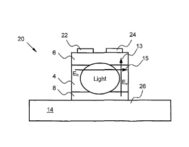
Figure 2 shows a schematic cross-sectional illustration of an electro-optic
waveguide
polarisation modulator according to one embodiment of the present invention.
The
waveguide polarisation modulator 20 according to the present embodiment
comprises a
deep-etched waveguide having a waveguide core 4 arranged between a first
cladding
layer 6 and a second cladding layer 8, the device being supported on a
substrate 14.
Without limitation, the modulator 20 is fabricated from III-V semiconductor
materials
using conventional metallorganic vapour phase epitaxy (MOVPE) and molecular
beam
epitaxy (MBE) processes. Specifically, the first cladding layer 6 and the
second
cladding layer 8 comprise gallium aluminium arsenide (AlGaAs) alloy whereas
the
waveguide core 4 and the substrate typically comprise gallium arsenide (GaAs).
Whereas the conventional waveguide polarisation modulator 2 merely comprises
first
and second electrodes 10, 12 for establishing a vertical electric field 13
within the
waveguide core 4, the waveguide polarisation modulator of the present
embodiment
has first and second electrodes 22, 24 arranged on the first cladding layer 6
and a third
electrode 26 arranged on the second cladding layer 8. The first and second
electrodes
22, 24 are arranged on the first cladding layer 6 in an area defined
substantially by the
horizontal extent of the electromagnetic field of electromagnetic waves
travelling within
= 30 the underlying electro-optic waveguide core 4. For example, in this
embodiment the
first and second electrodes 22, 24 are arranged on the top surface of the deep-
etched
waveguide and directly above the region of the electro-optic waveguide core 4
within
which the electromagnetic waves travel. The region of the substrate 14 in the
vicinity of
the second cladding layer 8 is arranged to be substantially conductive (for
example,
this region of the substrate may be arranged to be n-type by introducing
dopants
CA 02667145 2009-04-20
WO 2008/032048 PCT/GB2007/003431
- 14 -
therein) and therefore operates as the third electrode 26. Alternatively, the
second
cladding layer 8 may be substantially conductive so as to act as the third
electrode.
In this embodiment, inclusion of first and second electrodes 22, 24 on the
first cladding
layer 6 enables an electric field having field components 13, 15 in two
mutually
orthogonal directions (e.g. substantially vertical and horizontal directions)
to be created
within the waveguide core 4.
Application of a first modulation voltage Vi to the first electrode 22 and a
second
modulation voltage V2 to the second electrode 24, with respect to the third
common
electrode 26, enables independent control of the vertical and horizontal
electric field
components 13, 15 within the waveguide core 4.
The creation of such an electric field within the waveguide core 4 using
substantially
coplanar electrodes arranged in spaced relation to the waveguide core 4 has
not
hitherto been thought feasible. Rather, waveguide polarisation modulators
described in
the prior art have traditionally made use of drive electrodes arranged in a
plane which
includes the waveguide core 4 to ensure that the electric field extends fully
into the
waveguide core 4, and to maintain sufficient field strength therein to
modulate the
phase of electromagnetic radiation propagating through the core 4 (see N.
Grossard,
H. Porte, J. P. Vilcot, Bruno Beche and J. P. Goedgebuer, "AlGaAs-GaAs
Polarization
Converter with Phase Mismatch Control," IEEE Photon. TechnoL Lett., vol. 13,
pp. 830-
832, 2001).
By way of further explanation of the operation of the present modulator 20,
the vertical
component (E,) 13 of the applied electric field enables the refractive index
of the
waveguide core 4 to be modulated in the horizontal direction, while leaving
the
refractive index for vertically polarised light unchanged. The horizontal
component (Eh)
15 of the electric field enables the refractive index of the crystal in the
waveguide core
4 to be modulated such that a simultaneous change for the directions +450 and -
45
occurs with opposite sign, while there is no change for the horizontal and
vertical
directions. Consequently, the radius of the refractive index ellipsoid of the
waveguide
core 4 in the x, y, and z directions, and the alignment of the optical
electric fields of the
polarised modes within the waveguide are both variable in response to the
applied
modulation voltages V1 and V2.
CA 02667145 2009-04-20
WO 2008/032048 PCT/GB2007/003431
- 15 -
Note, the presence of metallic electrodes 22, 24 deposited on top of the
waveguide
forms a Schottky barrier diode at each electrode, which must be reverse-biased
if the
applied voltage is to be dropped across the optical region. It is therefore
only possible
to apply electric fields in the single vertical direction v, and horizontal
directions h, and
minus h.
Accordingly, the configuration of the electrodes in the polarisation modulator
20 of
figure 2 enables independent control of the angles of the polarised modes of
the
waveguides and the difference between the effective indices of those modes.
Accurate
polarisation control from a horizontal polarisation input state is therefore
possible.
Indeed, the modulator is capable of converting any input polarisation state to
any
output polarisation state. This means that the modulator is capable of
changing the
polarisation state from any start point to any end point on the Poincare
sphere.
By way of an example, a simple function that the waveguide polarisation
modulator 20
can perform is to convert a horizontal linearly polarised input state to a
vertical linear
output state. To do this, an offset voltage Voffset is applied between the
first and second
electrodes 22, 24 and the third electrode 26 to create a substantially
vertical electric
field which alters the effective index of the horizontal polarisation mode to
match it to
that of the vertical polarisation mode. This value of the offset voltage
Voffset is also
referred to herein as the phase-matching voltage. The phase matching voltage
eliminates any waveguide birefringence inherent in the polarisation modulator
20. The
modes of the waveguide may now be considered to be polarised at angles of +45
and
-45 .
The polarisation modulator 20 is designed such that any inherent waveguide
birefringence may be eliminated by applying a phase-matching voltage below the
Schottky barrier diode reverse bias breakdown voltage, which is typically in
the range
60 V to 80 V. Mindful that the electric fields can only be applied in a single
vertical
direction due to the Schottky barrier diode at each electrode 22, 24, the
waveguide
birefringence inherent in the polarisation modulator must be arranged to have
the
correct sign. The orientation of the polarisation modulator on the substrate
14 wafer
also affects whether the horizontal refractive index reduces, remains
unchanged, or
increases with applied electric field. Factors affecting the waveguide
birefringence
include the depth of the waveguide core 4, the refractive index step between
the
CA 02667145 2009-04-20
WO 2008/032048 PCT/GB2007/003431
- 16 -
cladding 6, 8 and the waveguide core 4, waveguide width and etch depth. The
invention permits the variation of all of these parameters, which may
therefore be
optimised so that the required phase-matching voltage has a specified value.
In
practice this may be required to meet the constraints imposed by electronic
drive
circuits.
A differential signal voltage Vsignal is also applied between the first and
second
electrodes 22, 24, while maintaining the mean of the voltages applied to first
and
second electrodes 22, 24 at the phase-matching voltage. This creates an
electric field
component 15 in a substantially horizontal direction which induces a
difference
between the effective refractive indices of the 45 modes, resulting in a
relative phase
shift. Given a horizontal input polarisation, these modes contain equal
amounts of
power so accurate conversion to a vertical output state occurs. The
differential signal
voltage Vsignal is chosen to produce such a conversion in the available length
of
waveguide. Alternatively, the differential signal voltage Vsignal is adjusted
to give a
circular or elliptical output polarisation. Possible output polarisations
include states
containing both horizontal and vertical components in any ratio.
The above function of the waveguide polarisation modulator 20 of the present
invention
may also be considered in terms of coupled-mode theory, where horizontal and
vertical
modes are assumed, but coupling between them is permitted in the presence of a
coupling mechanism. The maximum conversion efficiency is dependent on the
difference between the horizontal and vertical effective refractive indices,
which is
controlled by the vertical electric field component 13 provided by the offset
voltage
Voffset= The rate of coupling is controlled by the strength of the coupling
mechanism
which is controlled by the horizontal electric field component 15 provided by
the
differential signal voltage, Vsignal= Similar control is available with a
linear vertical input
state.
The present polarisation modulator 20 has the advantage that it may be
fabricated
using a standard process without any additional processing stages.
Accordingly, it may
be integrated with other waveguide structures including devices which require
a
horizontal polarisation state, such as a Mach-Zehnder interferometer intensity
modulator. Because of the enhanced degree of control offered by the present
electrode
arrangement, the fabrication tolerances are no more demanding than those for
other
CA 02667145 2009-04-20
WO 2008/032048 PCT/GB2007/003431
- 17 -
waveguide devices which have been fabricated successfully and repeatably. For
the
same reason, one device design may be used with a range of wavelengths.
..
Another embodiment of the present electro-optic waveguide polarisation
modulator is
shown in cross-section in figure 3. The structure of the device is similar to
that of figure
2, however an additional cap layer 30 is provided between the electrodes 22,
24 and
the first cladding layer 6. The embodiment of figure 3 also incorporates a
plurality of
second cladding layers 8a, 8b, 8c and a buffer layer 32 to decouple the device
from the
substrate 14. In this embodiment, the silicon doped layers 8a, 8b, 8c of the
lower
cladding provide third electrode 26. The design of the multiple lower cladding
layer
structure is optimised to allow only the fundamental spatial modes to
propagate with
low loss, while higher order modes leak into the substrate. Accurate control
of the
output state requires that only the fundamental modes are present at the
output.
The dimensions of the polarisation modulator are as follows; waveguide width
5.00 pm,
electrode width 1.0 pm, electrode separation (denoted in the figures by
numeral 34) 3.0
pm, etch depth (denoted in the figures by numeral 36) 4.4 pm, waveguide length
3.0
cm, wavelength of operation 1550 nm.
The composition of the semiconductor material comprising each of the various
layers
within the polarisation modulator is shown in Table 1.0 below.
Layer name Thickness AlGaAs Doping
(pm) composition
(% Al)
Cap 30 0.1 0 n- (minimised)
Upper cladding 6 1.2 20 n- (minimised)
Core 4 2.4 0 n- (minimised)
Lower cladding 8a 0.3 20 n- (minimised)
Lower cladding 8b 0.4 30 ¨1.0 x 10¹⁸/ cm3 silicon
doped
Lower cladding 8c 3.6 5.5 ¨5.0 x 10¹⁷ / cm3 silicon
doped
Buffer 32 0.2 0 ¨5.0 x 10¹⁷ / cm3 silicon
doped
Substrate 14 650 0 None
Table 1.0
CA 02667145 2009-04-20
WO 2008/032048 PCT/GB2007/003431
- 18 -
The polarisation modulator 20 was designed to operate at a wavelength of 1.55
ilm,
although it is potentially applicable to a wide range of other wavelengths,
for example
including 0.61.1m ¨ 17 ilm in GaAs.
The waveguide birefringence inherent in the present polarisation modulator was
arranged so that the refractive index for the horizontal polarisation
component was
larger than that of the vertical polarisation component. Hence, the
propagation direction
was selected to coincide with the [011] crystallographic direction on the
substrate 14,
while the vertical direction corresponded with the [100] crystallographic
direction. This
configuration enables the refractive index for the horizontal polarisation
component to
be reduced upon application of the phase-matching voltage. A phase-matching
voltage
of 39 V was found to be sufficient to eliminate the waveguide birefringence
inherent in
experimental polarisation modulators according to the present invention.
However, this
can be reduced by configuring the epitaxy to have a smaller horizontal /
vertical index
difference at the chosen waveguide width.
A differential signal voltage Vsignal of 8 V was required to switch the output
polarisation
state between linear horizontal and vertical in the experimental polarisation
modulator
according to the present invention. The operation of the device with Vsignal
greater than
V was demonstrated without electrical breakdown occurring.
The effect of applied fields on the refractive index of the material is
illustrated
diagrammatically in figure 4 which shows sections through the refractive index
ellipsoid
25 for the electro-optic waveguide polarisation modulator of figure 3.
Figure 4 illustrates
the refractive index ellipses for the waveguide core 4 resulting from applying
electric
fields in the vertical direction v, and horizontal directions h and minus h.
The ellipses
are shown for propagation along the crystallographic direction [011], while
the vertical
direction corresponds with the [100] crystallographic direction. The zero
birefringence
ellipse is denoted by a circle. Note, the ellipticity is greatly exaggerated
in the figure to
assist visualisation of the refractive index ellipsoid.
Figure 5 illustrates the response of the electro-optic waveguide polarisation
modulator
of figure 3. Specifically, figure 5 is an oscilloscope trace showing the
output optical
signal 46, 48 from the polarisation modulator with a horizontal input
polarisation at a
CA 02667145 2009-04-20
WO 2008/032048 PCT/GB2007/003431
- 19 -
wavelength of 1550 nm. Linear ramp voltages 40, 42 with opposite gradients
were
applied to the first and second electrodes 22, 24 respectively such that their
mean 41
was constantly equal to the phase-matching voltage. The differential signal
voltage
Vsignal is given by the difference between the two. The device output was
analysed
using a Glan-Taylor polariser and a detector. The horizontal 46 and vertical
48
polarisation output signal levels are shown, indicating the switch in the
output from
horizontal 46 to vertical 48 polarisation state, which requires an 8V change
in the signal
voltage. At the horizontal state peak, the horizontal / vertical polarisation
extinction ratio
was 20 dB. At the vertical state peak the horizontal / vertical polarisation
extinction ratio
was 13 dB. The voltage signals are plotted on a scale of 10 V per division.
Another embodiment of the present electro-optic waveguide polarisation
modulator is
show in cross-section in figure 6. The structure of the device is similar to
that of figure
2, however an additional lower electrode 28 is provided on the second cladding
layer 8.
The provision of fourth electrode 28 facilitates control of the vertical and
horizontal
electric fields within the device.
The foregoing embodiments may be used for switching speeds up to about 1 GHz,
however for faster switching frequencies the voltage applied to the electrodes
22, 24,
26, 28 must be treated as a radio frequency (RF) signal, as its wavelength is
less than
one order of magnitude longer than the electrode. A simple lumped electrode
will not
respond quickly enough in this case, so the electrical aspects of the
polarisation
modulator must be designed for microwave operation. Travelling-wave electrode
structures are well-proven in similar GaAs devices such as Mach-Zehnder
interferometer intensity modulators. These involve an RF transmission line
which is
designed to carry the signal at a group velocity which is matched to that of
the light, so
that the optical group is subject to the same refractive index distribution
throughout its
transit along the waveguide. Additionally the transmission line is designed
with a
characteristic impedance which matches that of the RF signal source and
termination.
This is often 50 a These proven designs are compatible with the present
waveguide
polarisation modulator described herein.
Accordingly, the present waveguide polarisation modulator may be configured as
a
travelling-wave device with coplanar strip line (CPS) electrodes, allowing
switching
speeds of 40 GHz or more. Hence, the present polarisation modulator may be
integrated with other waveguide structures including devices that require a
horizontal
CA 02667145 2009-04-20
WO 2008/032048 PCT/GB2007/003431
- 20 -
polarisation state, such as a Mach-Zehnder interferometer intensity modulator.
This is
not possible with the conventional single-electrode polarisation modulator of
figure 1 on
its own, because it is not compatible with a horizontal input polarisation
state.
Alternative configurations of the polarisation modulator are envisaged in
which the twin-
electrode polarisation modulator 20 is operated in a restricted mode,
requiring the
application of only one time-varying voltage signal. Such operation may be
convenient
in certain circumstances, including operation at RF switching speeds. Many
applications of these types of devices do not require full functionality, for
example fast
horizontal-vertical polarisation conversion has applications in optical
telecommunications, and this would only require the application of one RF
signal. Other
applications would use a fixed input polarisation. Accordingly, the present
polarisation
modulator may be configured in a number of different ways to enable different
degrees
of functionality.
Figure 7 shows a schematic block representation of a multiple-stage electro-
optic
waveguide polarisation modulator according to another embodiment of the
present
invention. In this embodiment, the electro-optic waveguide polarisation
modulator
comprises a twin-electrode polarisation modulator 20 followed by a
conventional single-
electrode device 2. The multiple stage device is capable of providing any
output
polarisation state on the Poincare sphere from a fixed input state. In this
case the twin
electrode stage 20 is not required to have full functionality. For the example
of a
horizontal linear input polarisation, the twin electrode stage 20 is operated
with a fixed
vertical electric field Ev to provide horizontal ¨ vertical phase matching,
while the
horizontal electric field Eh within the device is varied to convert any
proportion of the
light to vertical polarisation. This could be carried out at RF switching
speeds. The
single electrode stage 2 would then be used to alter the phase of the
horizontal
component relative to the vertical component. This could also be carried out
at RF
switching speeds. This example is of relevance to applications where the
device is to
be used immediately after a laser source.
If the input polarisation state is not fixed, and the twin-electrode stage 20
is to be
operated in restricted mode, then an additional single-electrode stage 2 is
required
before the twin-electrode stage 20 for all output states to be available. This
modulator
can change any input polarisation state on the Poincare sphere to any other
state on
the sphere. Figure 8 illustrates such a configuration comprising a
conventional single-
CA 02667145 2009-04-20
WO 2008/032048 PCT/GB2007/003431
- 21 -
electrode device 2, followed by a twin-electrode polarisation modulator 20 and
a further
a conventional single-electrode device 2. In this embodiment, the first single-
electrode
stage 2 shifts the phase of the horizontal component to n/2 relative to the
vertical
component. The second and third stages 20, 2 then operate as for the two-stage
device of figure 7 described above.
The electro-optic polarisation modulator according to the present invention
can be
configured in different ways (see figures 2, 6, 7, and 8) to enable the
modulation of the
polarisation state to any point on the Poincare sphere. This enables the
present
electro-optic polarisation modulator to operate as a transmitter within an
optical
communication system by modulating the polarisation state of an optical signal
transmitted thereby. Similarly, the present electro-optic polarisation
modulator can
operate as a receiver within such an optical communication system, enabling
the
polarisation state of a received optical signal to be determined.
When a polarised signal is transmitted between a transmitter and receiver part
of a
system either through optical fibre, or other waveguide medium or through a
gas or
vacuum or a combination of media, it is possible for the polarisation state to
be
distorted by rotation around the Poincare sphere. The modulator in this
invention
enables the correction of this distortion by applying either a compensating
pre-change
at the transmitter or a post-change at the receiver following measurement of
the
change.
By way of a further example application, the present polarisation modulator 20
finds
application in quantum cryptography (QC) applications where it offers a unique
combination of properties that enhance the performance of a QC system; namely
the
ability to modulate the polarisation over a range of states, ability to
modulate
polarisation at very high repetition rates and compact design with a single
laser source.
In addition it inherently provides more security than previously known QC
designs that
use multiple independent light sources for each polarisation state. Insecurity
arises with
the prior art QC designs that use multiple sources because it might be
possible to find
small differences in amplitude profile, the spatial profile, wavelength or
spectral
features and temporal characteristics such as pulse width, relative time
delays or
frequency chirping. By using a single light source in combination with the
present
polarisation modulator these potential differences are prevented.
CA 02667145 2009-04-20
WO 2008/032048 PCT/GB2007/003431
- 22 -
Some of the particular unique QC applications are outlined below. Note, only
some of
the QC protocols are mentioned below but in principle the present waveguide
polarisation modulator is beneficial to be used for any protocol requiring
more than two
polarisation states.
With regard to the wavelength of operation, the waveguide polarisation
modulator can
be designed to operate within a wavelength range 0.6 1.1171 - 17.0 i_tm. The
polarisation
modulator can be used in free space systems or fibre-optic systems.
The present polarisation modulator can potentially modulate the polarisation
of an input
light source with four different output polarisation states suitable for
application to the
BB84 protocol used in quantum cryptography. The four polarisation states
required for
BB84 could be a combination from any of the three pairs of polarisation states
commonly used in QC applications; namely 0 and 90 , 45 and -45 , and left
and right
circular. Each pair is called a basis, and while the two states in each basis
are
orthogonal, the relative polarisations between different basis are non-
orthogonal.
Therefore it is possible that some implementations of QC protocols may use
other non-
orthogonal pairs.
Since the polarisation modulator is capable of providing six polarisation
states (0 and
90 , 45 and -45 , and left and right circular) it is suitable for the six-
state polarisation
protocol (see for example D.Bruss, 'Optimal eavesdropping in quantum
cryptography
with six states', Phys Rev Lett 81, p3018-3021 (1998); and H.Bechmann-
Pasquinucci,
N.Gisin, 'Incoherent and coherent eavesdropping in the 6-state protocol of
quantum
cryptography', Phys Rev A 59, p4238-4248 (1999)).
The present polarisation modulator is also suitable for continuously variable
state
polarisation modulation. This is a relatively new protocol that requires the
ability to vary
the number of polarisation states of a light source. Security is based on the
measurable
difference in intensities between each polarisation state being less than the
quantum
noise in the channel. A polarisation based scheme has not yet been knowingly
implemented but could be enabled by application of the current modulator of
figures 2,
6,7, or 8.
CA 02667145 2009-04-20
WO 2008/032048 PCT/GB2007/003431
- 23 -
The modulator of figures 2, 6, 7, and 8 can also be used in a QC receiver. For
example, part of the BB84 protocol requires that the receiver randomly select
the
measurement basis and then deterministically measure the polarisation state.
The
modulator can be used in a receiver by applying a random signal to switch
between
any two polarisation basis, for example to select either the -45 and 45
basis, or left-
circular and right-circular basis. This is achieved by selecting a single
voltage for each
basis, for example -45 or left-circular. In this way if either -45 and 45
polarisation is
incident on the modulator then the output is either -45 and 45 . Similarly if
left-circular
and right-circular is incident then -45 and 45 is also output. The output
polarisation
states can then be detected by a pair of detectors after a polarisation
beamsplitter
arrangement (not shown). The six-state protocol would operate in a similar way
but by
using one of three voltages to select each basis.
Implementation of QC in optical fibre has a well known problem that
polarisation
distortion causes problems for effective operation. The use of an additional
polarisation
modulator according to the present invention as described earlier either at
the
transmitter or receiver could be used to compensate for the distortions. This
could be
implemented with devices as shown in figures 2, 6, 7, and 8.
The present polarisation modulator 20 can also be used in a Light Detection
and
Ranging (LIDAR) system. A coherent LIDAR transceiver typically contains an
optical
source emitting linearly polarised light, followed by a series of optical
components that
permit the transmission of light, the collection of received light,
interference between
the received light and a local oscillator component of the light, and
detection of the
resulting optical signal. In order that the output aperture can also be used
as a receiver
aperture, a set of optical components is used to direct the received light
along a path to
interfere with the local oscillator light. This process requires several
polarisation
transformations, which are typically performed using a quarter-wave plate and
a half-
wave plate. In an integrated optical form of this system, the functions
performed by the
quarter-wave plate and a half-wave plate may be performed by two polarisation
modulators 20, with an appropriate choice of fixed voltages. This application
of the
polarisation modulator invention is enabled by the feature of the component
that it may
be fabricated using the same process as a range of other integrated optical
components.
CA 02667145 2009-04-20
WO 2008/032048 PCT/GB2007/003431
- 24 -
Although specific embodiments of the present electro-optic waveguide
polarisation
modulator have been described in terms of a gallium arsenide / gallium
aluminium
arsenide architecture, the modulator may be fabricated from other III-V
materials e.g.
indium gallium arsenide (InGaAs) alloys, indium gallium aluminium arsenide
phosphide
(InAlGaAsP) alloys, indium phosphide (InP), indium antimonide (InSb), gallium
nitride
(GaN); II-VI materials, lithium niobate, strained silicon or an electro-optic
polymer
material.
In view of the foregoing description it will be evident to a person skilled in
the art that
various modifications may be made within the scope of the invention.
The scope of the present disclosure includes any novel feature or combination
of
features disclosed therein either explicitly or implicitly or any
generalisation thereof
irrespective of whether or not it relates to the claimed invention or
mitigates any or all of
the problems addressed by the present invention. The applicant hereby gives
notice
that new claims may be formulated to such features during the prosecution of
this
application or of any such further application derived there from. In
particular, with
reference to the appended claims, features from dependent claims may be
combined
with those of the independent claims and features from respective independent
claims
may be combined in any appropriate manner and not merely in the specific
combinations enumerated in the claims.