Note: Descriptions are shown in the official language in which they were submitted.
CA 02668973 2009-05-05
-1-
WO 2008/055579 PCT/EP2007/008948
Description
Chip module for an RFID system
The invention relates to a chip module for an RFID
system, in particular for an RFID label, a coupling
label for use in an RFID label, an RFID inlay for an
RFID label, and an RFID label produced using an RFID
inlay (smart label).
In the production of RFID labels, use is made in a
known manner of chip modules having an RFID microchip
and electrical connection contacts by means of which
they are connected to the RFID antenna. WO 2005/076206
describes a continuous production method for RFID
labels in which the chip modules are applied by their
rear side remote from the connection coritacts to
adhesive film sections whose base area is in each case
significantly larger than a base area of each chip
module. The electrical connection contacts of the chip
modules are electrically contact-connected to the
antenna connections, the adhesive film sections being
connected to the antenna film sections in planar
fashion in such a way that the chip modules are
positionally fixed relative to the antenna connections.
RFID labels are produced in a known manner in such a
way that a so-called RFID inlay is arranged between the
web-type covering material, which is provided with a
pressure-sensitive adhesive layer on the underside, and
a likewise web-type carrier material that can be
stripped from the pressure-sensitive adhesive layer.
The RFID inlay contains an RFID chip that is fixed on a
flat antenna and is galvanically connected thereto, the
RFID antenna being arranged on an antenna film.
It is known to fix the chip modules for processing in a
series one behind another on strips and to supply them
CA 02668973 2009-05-05
WO 2008/055579 PCT/EP2007/008948
- 2 -
to the RFID antennas in this way during processing.
Each microchip with its two connection contacts is then
stripped from the strip and fixedly adhered on the RFID
antenna in such a way that its connection contacts have
galvanic contact with the contacts of the RFID antenna.
This step necessitates positioning the chip modules
very exactly on the RFID antenna in order that the
galvanic contact is produced.
Therefore, the invention is based on the object of
providing a chip module which can be brought into
contact with the RFID antenna in a simplified manner.
This object is achieved according to the invention by
virtue of the fact that an RFID chip and a coupling
antenna that is electrically, in particular
galvanically, connected to the RFID chip are arranged
on a web- or sheet-type carrier material, in particular
on a carrier film.
The coupling antenna makes it possible to produce an
inductive connection to the RFID antennas. An inductive
connection can be produced in a simplified manner
through corresponding configuration of the coupling
antenna and the RFID antenna without both of them
having to be positioned very exactly with respect to
one another, particularly if the coupling region of the
RFID antenna is wider than the coupling region of the
coupling antenna. The chip module can be adhesively
bonded onto the corresponding location of the RFID
antenna with a defined distance determined by the
thickness of the carrier film and of the pressure-
sensitive adhesive layer.
A further advantage afforded is that the RFID chip can
be arranged on the coupling antenna in a simplified
=t
CA 02668973 2009-05-05
WO 2008/055579 PCT/EP2007/008948
- 3 -
manner without the need for complicated connection
contacts for later connection to the RFID antenna.
The RFID antenna can advantageously be produced as a
flat, for example etched or printed antenna from the
customary antenna materials, and is advantageously
arranged on a carrier film, in particular an adhesive
material.
A so-called coupling label can advantageously be
produced from the chip module according to the
invention, said coupling label being used in the
subsequent production of RFID systems, in particular
RFID labels, tags or tickets. In the case of the
coupling label, the underside of the carrier film of a
chip module has an adhesive layer covered by a
strippable web- or sheet-type separating material.
In this case, the coupling labels can advantageously be
produced in strip form with a plurality of chip modules
arranged at a distance one behind another. During the
production of RFID systems, they are supplied in this
way on strips into respective RFID antennas and either
they are fixed in strip form on the antennas, which are
likewise arranged in strips, or they are separated from
the strip and individually bonded adhesively onto an
antenna.
If the coupling labels are used for producing RFID
labels, then preferably a so-called RFID inlay is
firstly produced. The RFID inlay comprises a flat RFID
antenna, which is preferably arranged on an antenna
film and onto which a chip module according to the
invention is adhesively bonded by its carrier film in a
manner positioned such that the coupling antenna and
the RFID antenna are inductively coupled. Preferably,
the antenna film has on its rear side a pressure-
sensitive adhesive layer covered by a separating
CA 02668973 2009-05-05
WO 2008/055579 PCT/EP2007/008948
- 4 -
material. The RFID label is then produced in such a way
that an RFID inlay according to the invention is
arranged between a web- or sheet-type covering
material, which is provided with a pressure-sensitive
adhesive layer on the underside, and a web- or sheet-
type separating material that can be stripped from the
pressure-sensitive adhesive layer in order to uncover
the latter for the adhesive bonding of the label. The
covering material can be printed or configured
graphically in some other way at its top side.
The chip module according to the invention can
advantageously also be used in other RFID systems.
Thus, the coupling label can be adhesively bonded onto
an RFID antenna that has been applied, for example
printed, onto the packaging means. The coupling antenna
is then inductively coupled to the RFID antenna (6) of
the packaging means (smart box).
The invention is explained in more detail below on the
basis of an exemplary embodiment illustrated in
simplified fashion.
Figure 1 shows an individual coupling label each
having a chip module and their positioning on
antennas for producing RFID inlays.
Figure 2 shows RFID inlays to which coupling labels in
strip form are supplied.
Figure 3 shows a section through an RFID inlay.
Figure 1 illustrates two coupling labels 1 each
containing a chip module2 having an RFID chip 3. The
RFID chip 3 is arranged on a coupling antenna 4 and is
electrically, in particular galvanically, connected
thereto. The coupling antenna 4 with the RFID chip 3 is
arranged on a web- or sheet-type carrier material, in
CA 02668973 2009-05-05
WO 2008/055579 PCT/EP2007/008948
- 5 -
particular a carrier film 5. Preferably, the RFID chip
3, as illustrated in figures 1 to 3, is directly fixed
on the coupling antenna 4 formed in planar fashion and
is galvanically connected thereto. In order to produce
a self-adhesive coupling label, the underside of the
carrier film 5 of a chip module 2 has an adhesive layer
9 covered by a strippable web- or sheet-type separating
material 11. After the separating material 11 has been
stripped off, the coupling label 1 can thus be
adhesively bonded onto an RFID antenna 6. In this case,
the coupling antenna 4 adhesively bonded on maintains a
precisely defined distance from the RFID antenna 6. The
distance is chosen such that the coupling antenna 4 and
the RFID antenna 6 are inductively coupled. It can be
set exactly by way of the thickness of the carrier film
5 and the adhesive layer 9 thereof. Preferably, each
RFID antenna 6 is arranged on an antenna film 7. As
illustrated in figures 1 and 2, a plurality of RFID
antennas 6 are advantageously arranged at a distance
from one another on a strip-type antenna film 7 in
order to produce RFID inlays which are connected to one
another and which can be supplied for further
processing in a simplified manner.
Preferably, the coupling region 6.1 of the RFID antenna
6 is wider than the coupling region 4.1 of the coupling
antenna 4. This provides a certain leeway for
positioning the coupling region 4.1 of the coupling
antenna 4 on the coupling region 6.1 of the RFID
antenna 6. Leeway for the positioning of the coupling
labels 1 on the antennas 6 is thus obtained in the
production of the RFID inlays.
In the case of the procedure illustrated in figure 1,
the coupling labels 1 with the chip modules 2 are
supplied individually in each case to the RFID antennas
6. After stripping off the respective separating film
on the underside, the adhesive layer 9 of the carrier
CA 02668973 2009-05-05
WO 2008/055579 PCT/EP2007/008948
- 6 -
film 5 is uncovered, and a respective chip module 2 is
adhesively bonded onto an RFID antenna 6.
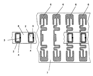
It is likewise possible - as illustrated in figure 2 -
to arrange a series of chip modules 2 on a strip-type
carrier film 8 at a distance from one another. In this
case, the distance between the chip modules 2
corresponds to the distance between the RFID antennas 6
on the carrier film 7 thereof. After stripping off the
separating material from the underside, the adhesive
layer is uncovered on the carrier film 8 and the chip
modules 2, still situated on a common carrier film 8,
are continuously bonded adhesively onto the antennas 6.
The division into individual RFID inlays is
subsequently effected by means of transverse cuts
between the individual antennas 6, only the antenna
film 7 being severed in the case of the procedure
according to figure 1. In the case of the procedure
according to figure 2, the antenna film 7 and the
carrier film 8 are each severed jointly.
The RFID antenna 6 can likewise be an antenna which is
applied, in particular printed, directly onto a
packaging means, for example a folding box, and onto
which the coupling label 1 is adhesively bonded (smart
box).
The construction of the RFID inlay according to the
invention is illustrated in clarified fashion in figure
3: the RFID chip 3 is fixed directly on the coupling
antenna 4. The coupling antenna 4 is situated on the
top side of a carrier material 5 having an adhesive
layer 9 on its underside. The carrier material 5 with
the coupling antenna situated thereon and with the chip
3 is fixedly adhered on the RFID antenna 6 by means of
the adhesive layer 9. Depending on the intended use,
the RFID antenna 6 is an HF or UHF antenna. The RFID
antenna 6 is fixed on the top side of the antenna film
CA 02668973 2009-05-05
WO 2008/055579 PCT/EP2007/008948
- 7 -
7, and the antenna film 7 has on its underside a
pressure-sensitive adhesive layer 10 covered by a
strippable separating material 11, for example a
silicone carrier.
In order to produce an RFID label, the RFID inlay
illustrated in figure 3 is arranged between a web- or
sheet-type covering material and a likewise web- or
sheet-type carrier material. The covering material,
which is usually printed on the top side, has on its
underside a pressure-sensitive adhesive layer, onto
which the carrier material is adhesively bonded in
strippable fashion. In order to introduce the RFID
inlay between the covering material and the carrier
material of the label, the carrier material is lifted
off and put down again after the RFID inlay has been
fixedly adhered on the pressure-sensitive adhesive
layer. The separating material 11 of the RFID inlay is
removed beforehand, such that a continuous adhesive
layer is present below the carrier material of the RFID
label, which is composed of silicone paper, for
example. The RFID label configured in this way can be
adhesively bonded onto an item of merchandise or a
packaging after the carrier material has been stripped
off.