Note: Descriptions are shown in the official language in which they were submitted.
CA 02669224 2009-05-11
WO 2008/127429 PCT/US2007/085199
SYSTEM FOR ASSEMBLING AND UTILIZING SENSORS IN CONTAINERS
Cross-Reference to Related A1212lications
This application claims priority to United States provisional patent
application
number 60/866,714 filed November 21, 2006; the entire disclosure of which is
incorporated herein by reference in its entirety.
Field of the Invention
This invention relates to a system for assembling and utilizing sensors in
containers.
Backaound of the Invention
In order to keep humans safe from solutions, such as liquid, gas and solid
that
may be toxic or harmful to them different devices are used to test the
solutions to
determine if they are harmful. These devices include chemical or biological
sensors
that attach an identification marker with an antibody. For example, some
chemical/biological sensors include a chip attached to an antibody, where the
chip
includes fluorescent markers identifying the specific antibody.
There are known chemical or biological sensors that include structural
elements that are formed from a material that selectively responds to a
specific
analyte as shown in U.S. Patent No. 6,359,444. Other known chemical or
biological
sensors include an electromagnetically active material that is located in a
specific
position on the sensors that may be altered by an external condition as
indicated in
U.S. Patent No. 6,025,725. Some known chemical or biological sensor systems
1
CA 02669224 2009-05-11
WO 2008/127429 PCT/US2007/085199
include components for measuring more than one electrical parameters as shown
in
U.S. Patent No. 6,586,946.
While the aforementioned sensors can be used to measure electrical
parameters, a single use disposable bio-processing system utilizing these
sensors has
not been developed. While the disposable bio-processing systems and
technologies
may be readily used, their acceptance is hindered by the absence of effective
single
use, non invasive monitoring technologies. Monitoring of key process
parameters is
crucial to secure safety, process documentation and efficacy of the produced
compounds as well as to keep the process in control. The utilization of in-
line non-
invasive disposable sensor technologies for multi-parameter in-line reading in
disposable bio-processing assemblies will enable safe and fast production
deployment
because it allows a flawless uptake of disposable purification strategies and
will
eliminate expensive and time wasting off-line analytics. Therefore, there is a
need for
a system that enables the user to simply and non-invasively test for chemical
and/or
biological material in a solution in a disposable bio-processing system where
the user
can safely obtain measurements for the material, then dispose of the bio-
processing
system.
Brief Summary of the Invention
The present invention has been accomplished in view of the above-mentioned
technical background, and it is an object of the present invention to provide
a system
and method for assembling and utilizing sensors in a container.
In a preferred embodiment of the invention, there is a system for measuring
multiple parameters. A container has a solution. A protective layer is
deposited over
at least one sensor and at least one wall of the container, where the
protective layer is
2
CA 02669224 2009-05-11
WO 2008/127429 PCT/US2007/085199
attached to the wall of the container to form a seal between the container and
the at
least one sensor. The at least one sensor is configured to have an operable
electromagnetic field based on a thickness of the container and the protective
layer.
The at least one sensor in conjunction with a digital identification tag is in
proximity
to an impedance analyzer and a reader that constitute a measurement device.
The at
least one sensor is configured to determine at least one parameter of the
solution. The
tag is configured to provide a digital ID associated with the at least one
sensor, where
the container is in proximity to the reader and an impedance analyzer. The
impedance
analyzer is configured to receive a given range of frequencies from the at
least one
sensor based on the parameter and calculate parameter changes based on the
measured
complex impedance over the given range of frequencies.
In another preferred embodiment of the invention, a method for assembling a
system for measuring parameters is disclosed. At least one sensor is provided,
where
the at least one sensor is placed in between a first layer of film and a
second layer of
film. The first layer of film and the second layer of film are provided with a
certain
thickness, where the at least one sensor is configured to have an operable
electromagnetic field. The second layer is formed over the at least one sensor
into the
first layer, where the second layer is formed over the at least one sensor
into the first
layer to embed the at least one sensor into the first layer. A third layer of
film is
provided, where the third of layer of film is formed into the first layer of
film that is
configured to form a container with the third layer of film. A solution is
provided into
the container, where the first layer of film and the at least one sensor are
configured to
measure at least one parameter of the solution.
3
CA 02669224 2009-05-11
WO 2008/127429 PCT/US2007/085199
Brief Description of the Drawings
These and other advantages of the present invention will become more
apparent as the following description is read in conjunction with the
accompanying
drawings, wherein:
FIG. 1 illustrates a block diagram of a system for assembling and utilizing
sensors in a container in accordance with an embodiment of the invention;
FIGs. 2A and 2B illustrate the sensor embedded into the container in
accordance with an embodiment of the invention;
FIG. 3 illustrates an exploded view of the radio frequency identification
(RFID)
tag of FIG. 1 in accordance with the invention;
FIGs. 4A, 4B, 4C and 4D are schematic diagrams of circuitry for RFID
systems constructed in accordance with the invention;
FIG. 5 depicts a flow chart of how the sensors are incorporated into the
container by employing ultrasound welding in accordance with the invention;
FIG. 6 depicts a flow chart of how the sensors are incorporated into the
container by employing radio frequency welding in accordance with the
invention;
FIG. 7 depicts a flow chart of how the sensors are incorporated into the
container by employing heat lamination in accordance with the invention;
FIG. 8 depicts a flow chart of how the sensors are incorporated into the
container by employing hot plate welding in accordance with the invention;
FIG. 9 depicts a flow chart of how the sensors are incorporated into the
container by employing injection mold thermoplastics in accordance with the
invention;
FIGs. l0A and l OB illustrate a sensor in silicon tubing in accordance with
the
invention;
4
CA 02669224 2009-05-11
WO 2008/127429 PCT/US2007/085199
FIG. 11 shows an example of sensors in accordance with the invention;
FIG. 12 illustrates an example of measuring the sensor in accordance with the
invention;
FIG. 13 is a graphical representation of a dynamic response and response
magnitude from FIG. 12 in accordance with the invention; and
FIG. 14 is a graphical illustration of a calibration curve of FIG. 12 in
accordance with the invention.
Detailed Description of the Invention
The presently preferred embodiments of the invention are described with
reference to the drawings, where like components are identified with the same
numerals. The descriptions of the preferred embodiments are exemplary and are
not
intended to limit the scope of the invention.
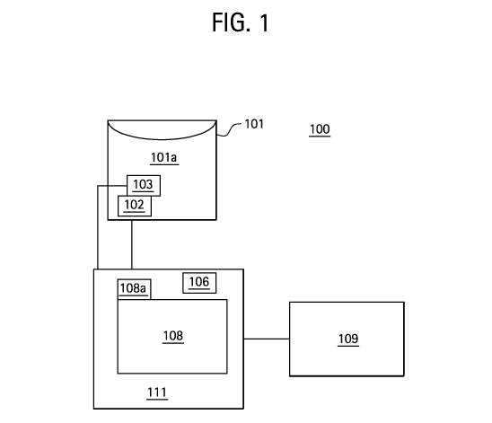
FIG. 1 illustrates a block diagram of a system for measuring parameters in a
container. The system 100 includes a container 101, a tag 102 and a sensor 103
on
the tag 102, a reader 106, an impedance analyzer 108, a standard computer 109
and a
measurement device 111. Measurement device 111 includes the reader 106 and the
impedance analyzer 108. Impedance analyzer 108 includes a pickup antenna 108a,
which excites the plurality of RFID sensors in the array 103 and the pickup
antenna
108a collects a reflected radio frequency signal from the plurality of RFID
sensors in
the arrays 103. The tag 102 and the sensor 103 are incorporated or integrated
into the
container 101. Several sensors 103 or a plurality of sensors 103 may be formed
on
the tag 102 in an array format. The sensor 103 or sensor array 103 is
incorporated
into container 101, which is connected by a wireless connection or an
electrical wire
connection to the impedance analyzer 108 and the computer 109. The sensor 103
or
5
CA 02669224 2009-05-11
WO 2008/127429 PCT/US2007/085199
sensor array 103, the tag 102 are connected by a wireless connection or an
electrical
wire to the measurement device 111 and the computer 109. Impedance analyzer
108
is connected by a wireless connection or an electrical wire connection to the
computer
109.
Referring to FIGs. 2A and 2B, container 101 may be a disposable bio-
processing container, a stainless steel container, a plastic container, a
polymeric
material container, a chromatography device, a filtration device, a
chromatography
device with any associated transfer conduits, a filtration device with any
associated
transfer conduits, centrifuge device, centrifuge device with any associated
transfer
conduits, a pre-sterilized polymeric material container or any type of
container
known to those of ordinary skill in the art. In one embodiment, the biological
container 101 is preferably made from but not limited to the following
materials,
alone or in any combination as a multi-layer film: ethylene vinyl acetate
(EVA) low
or very low-density polyethylene (LDPE or VLDPE) ethyl-vinyl-alcohol (EVOH)
polypropylene (PP), polyethylene, low-density polyethylene, ultra-low density
polyethylene, polyester, polyamid, polycarbontate, elastomeric materials all
of which
are well known in the art. RFID tags typically comprise front antennas and
microchip
with a plastic backing (e.g., polyester, polyimide etc).
Also, the container 101 may be made of a multilayer bio-processing film,
made from one manufacturer. For example, the manufacturer may be Hyclone
located in Logan, Utah, for example HyQ CX5-14 film and HYQ CX3-9 film.
The CX5-14 film is a 5-layer, 14 mil cast film. The outer layer of this film
is made of
a polyester elastomer coextruded with an EVOH barrier layer and an ultra-low
density
polyethylene product contact layer. The CX3-9 film is a 3-layer, 9mil cast
film. The
outer layer of this film is a polyester elastomer coextruded with an ultra-low
density
6
CA 02669224 2009-05-11
WO 2008/127429 PCT/US2007/085199
polyethylene product contact layer. The aforementioned films may be further
converted into disposable bio-processing components in a variety of geometries
and
configurations all of which can hold a solution 10 l a. In yet another
embodiment of
the invention, the container 101 may be a polymer material incorporated into a
filtration device. Further, the container 101 may include or contain a
chromatographic matrix.
Depending on the material of the container, the sensor 103 or sensor array
103,
the tag 102 are connected by a wireless connection or an electrical wire to
the
measurement device 111 and the computer 109. Container 101 may also be a
vessel
that contains a fluid such as liquid or gas, where the vessel can have an
input and an
output. Further, container 101 can have a liquid flow or no liquid flow.
Furthermore,
container 101 can be a bag or a tube, or pipe, or hose.
The solution 10 l a may also be referred to as a bio-processing fluid. Inside
the
container 101 is the solution 10 l a. Solution 10 l a in the container 101 may
be stored
or for transfer. The solution 10 l a may be a liquid, fluid or gas, a solid, a
paste or a
combination of liquid and solid. For example, the solution 10 l a may be
blood, water,
a biological buffer or gas. The solution 10 l a may contain toxic industrial
material,
chemical warfare agent, gas, vapors or explosives disease marker in exhaled
breath,
bio-pathogen in water, virus, bacteria and other pathogens. If the solution
l0l a is
blood it may contain various materials such as creatinine, urea, lactate
dehydrognease,
alkaline phosphate, potassium, total protein, sodium, uric acid, dissolved
gases and
vapors, such as C02, 02, NOX, ethanol, methanol, halothane, benzene,
chloroform,
toluene, chemical warfare agents, vapor, living tissue, fractionated from a
biological
fluid, vaccine or explosives and the like. On the other hand if the solution
10 l a is a
gas or vapor, it may be C02, 02, NOX, ethanol, methanol, halothane, benzene,
7
CA 02669224 2009-05-11
WO 2008/127429 PCT/US2007/085199
chloroform toluene or chemical warfare agent. If the solution 10 l a is a
toxic
industrial agent that can be inhaled and dissolved in blood then in may be
ammonia,
acetone cyanohydrin, arsenic tricholoride, chlorine, carbonyl sulfide or the
like. In
the case where the solution 101 a is a chemical war agent it may be Tabun,
Sarin,
Soman, Vx, blister agents, Mustard gas, choking agent or a blood agent. If the
solution 101 a is a disease marker in exhaled breath it may be acetaldehyde,
acetone,
carbon monoxide and the like. If the solution 10 l a includes a bio-pathogen
then it
may be anthrax, brucellosis, shigella, tularemia or the like. Further, the
solution 10 l a
in the container may include prokaryotic and eukaryotic cells to express
proteins,
recombinant proteins, virus, plasmids, vaccines, bacteria, virus, living
tissue and the
like. Container 101 may have many structures, for example, a single biological
cell,
a micro fluidic channel, a micro titer plate, a Petri dish, a glove box, a
hood, a walk-in
hood, a room in a building or a building. Thus, container 101 can be of any
size
where sensor 103 and tag 102 are incorporated into the container 101 where
they are
positioned to measure the environment in the container 101 or the solution 10
l a in the
container 101.
In close proximity to the solution 10 l a or in the solution 10 l a is the
plurality
of sensors in the array 103. The sensor array 103 is embedded, integrated or
incorporated to a wall 101b of the container 101 by any of the various
processes
described in FIGs. 5-9, such as ultrasonic welding, dielectric welding (also
known as
high frequency (HF) welding or radio frequency (RF) welding), laser welding,
hot
Plate welding, hot knife welding, induction/impulse, insert molding, in-mold
decoration and the other standard types of material welding and joining
methods
known to those of ordinary skill in the art.
8
CA 02669224 2009-05-11
WO 2008/127429 PCT/US2007/085199
The aforementioned processes are also utilized to deposit a protective layer
105 onto the sensor 103 as shown in FIGs. 2A and 2B. Protective layer 105 may
be a
barrier layer, a semi-permeable layer, or a perm-selective layer. This
protective layer
105 is used to prevent the components of the sensor 103 and optional sensor
coating
107, located in between the protective layer 105 and the sensor 103 (FIG. 2B)
from
discharging into the environment of the container 101 and keeps the solution
10 l a
from corroding the sensor 103 that allows for the proper chemical or
biological
recognition of the embedded sensor 103. Also, the protective layer 105
prevents the
bio-processing fluid (solution 10 l a) from contamination caused by any
leachable or
extractable that is present in the RFID sensor 103. The sensor coating 107 is
selected
for proper chemical or biological recognition. The typical sensor coating or
film 107
is a polymer, organic, inorganic, biological, composite, or nano-composite
film that
changes its electrical property based on the solution 10 1 a that it is placed
in. The
sensor film (or sensing coating) 107 may be a hydrogel such as (poly-(2-
hydroxyethyl)
methacrylate, a sulfonated polymer such as Nafion , , which is a registered
trademark
of DuPont located in Wilmington, DE, an adhesive polymer such as silicone
adhesive,
an inorganic film such as sol-gel film, a composite film such as carbon black-
polyisobutylene film, a nanocomposite film such as carbon nanotube-Nafion
film,
gold nanoparticle-hydrogel film, electrospun polymer nanofibers, metal
nanoparticle
hydrogen film electrospun inorganic nanofibers, electrospun composite
nanofibers,
and any other sensor material. These aforementioned materials for the sensor
film 107
may be deposited onto the sensor 103 by ink-jet printing, screen printing,
chemical
deposition, vapor deposition, spraying, draw coating, wet solvent coating,
roll-to-roll
coating, slot die, gravure coating, roll coating, dip coating etc. In order to
prevent the
material in the sensor film 107 from discharging into the container 101, the
sensor
9
CA 02669224 2009-05-11
WO 2008/127429 PCT/US2007/085199
materials are attached to the surface of the plurality of sensors array 103
using the
standard techniques, such as ion pairing, covalent bonding, electrostatic
bonding and
other standard techniques known to those of ordinary skill in the art. The
thickness of
the protective layer 105 is in a range of 1 nanometers to 300mm. The thickness
of the
wall 101b is in a range of 5 nanometers to 50 cm. Preferably, the wall 101b
has a
thickness of 10 cm. More preferably, the wall 101b has a thickness of 5cm or
even
more preferably, the wall 101b has a thickness of 1cm. However, if in-mold-
decoration/injection molding is used to make 3-D container with embedded
sensor,
the wall thickness could be significantly higher, for example up to 10cm.
This thickness for the protective layer 105 and the wall 101b is necessary for
the electro-magnetic field surrounding the sensor 103 to be operable and
retained
while it is within the container 101. A wireless integration of the sensor 103
with an
impedance analyzer 108 occurs when an electromagnetic field that is generated
around the sensor 103 when the impedance analyzer 108 is in proximity to the
sensor
103. Specifically, the electromagnetic field extends out of the plane of
sensor 103
into the direction of wall 101b and protective layer 105. Pickup antenna 108a
excites
the RFID sensor 103. In an embodiment, pickup antenna 108a is arranged on the
opposite side of wall 101b from sensor 103. In another embodiment, pickup
antenna
108a in proximity to the sensor 103 is arranged on the opposite side of
protective
layer 105 from sensor 103.
In order for the pickup antenna 108a to receive a signal from sensor 103 the
thickness and dielectric properties of the material of the protective layer
105, wall
101b and the optional sensing coating 107 between pickup antenna 108a and
sensor
103 must be adequate. In other embodiments of the invention, the pick-up
antenna
108a may be attached or connected to the container 101 in several ways: 1. the
pick-
CA 02669224 2009-05-11
WO 2008/127429 PCT/US2007/085199
up antenna is mechanically attached to the container 101, 2. the pick-up
antenna is
chemically attached to the container by any typical chemical means, such as an
adhesive, and 3. the pick-up antenna 108a is attached to the container 101 by
gravity.
In another embodiment of the invention, the pick-up antenna 108a is attached
to
container 101 without electrical contact with the sensor 103. The signal from
the
sensor 103 will be attenuated upon an increase of the distance between sensor
103 and
the pickup antenna 108a.
The signal from the sensor 103 will be changed, in general attenuated upon an
increase of the conductivity of material that is positioned between sensor 103
and
pickup antenna 108a. Thus, in general, under a constant realistic dielectric
property
of the wall l0lb or protective layer 105, the smaller the thickness of the
wall l0lb or
protective layer 105, the larger the signal will be from the sensor 103.
In order to provide a convenient way of positioning the pick-up antenna 108a
in proximity to the sensor 103, the pick-up antenna 108a is attached to the
container
101. In one embodiment, portions of the outer surface of the container 101 are
modified in the region where the RFID sensor 103 is embedded, so the pick-up
antenna 108a for the sensor 103 has a better stability control (position,
tilt, etc.). In
another embodiment, portions of the outer surface of the container 101 are
modified
in the region where the RFID sensor 103 is embedded, so the pick-up antenna
108a
for the sensor 103 has a better stability control by using mechanical
connections
(plastic nipples, clamps, etc.) at the corners, sides, etc. where the pickup
antenna 108a
snaps or connects otherwise into its appropriate position.
In yet another embodiment, portions of the outer surface of the container 101
are modified in the region where the RFID sensor 103 is embedded, so the pick-
up
antenna 108a for the sensor 103 has a better stability control by using an
adhesive
11
CA 02669224 2009-05-11
WO 2008/127429 PCT/US2007/085199
material so the pickup antenna 108a connects into its appropriate position on
the
container 101. In another embodiment, portions of the outer surface of the
container
101 are modified in the region where the RFID sensor 103 is embedded, so the
pick-
up antenna 108a for the sensor 103 has a better stability control by using the
gravity
force of the pick-up antenna 108a to better connect it into its appropriate
position on
the container 101. Other connection methods that do not use a galvanic or
direct
connection of wires between the pickup antenna 108a and sensor 103 can be used
by
those of ordinary skilled in the art.
Sensor 103 is covered by the protective layer 105 and the sensor coating 107.
If the aforementioned thicknesses of the protective layer 105 and the wall
101b are
not adhered to then the electromagnetic field surrounding the sensor 103 will
decay
and the sensor 103 will not be able to measure parameters of the solution 101.
The edges of the protective layer 105 are permanently attached, for example
by welding or lamination to the wall 101b of the container 101 to form a tight
seal.
The container 101 also known as the disposable bio-processing system with the
embedded sensor or sensor arrays 103 meet the requirements of
biocompatibility,
sterilizability, mechanical toughness, elasticity, and low leachability. This
protective
layer may also include dense plastic films, membranes, microporous layers,
mesoporous layers, such as expanded Polytetrafluoroethylene PTFE (e-PTFE),
nanofiltration and ultrafiltration membranes, can also be used as protective
layer or
perm-selective layer to reduce bio-fouling, concentrate the species to be
detected and
to provide corrosion resistance for the sensor 103 components. In another
embodiment of the invention, the protective layer 105 is a conductive polymer
film.
In yet another embodiment of the invention, the protective layer 105 may be a
composite film that may include a filled polymer, polymer blend and alloy.
This
12
CA 02669224 2009-05-11
WO 2008/127429 PCT/US2007/085199
composite film has the desired electric constant, electrical conductivity,
thermal
conductivity, permeability of dissolved gases such as oxygen and COz.
Reader 106 is located in the measurement device 111 outside of the container
101. An antenna 301 (FIG. 3) of tag 102 when covered by a polymer inorganic,
composite or other type of film nanofiber mesh or nanostructured coating is
the sensor
103 or the sensor array 103. Plurality of sensors in an array 103 can be a
typical
sensor or typical sensor array known to those of ordinary skill in the art or
the
plurality of sensors in an array may be radio frequency identification (RFID)
sensors
array 103. RFID sensors in the array 103 are devices that are responsible for
creating
a useful signal based on a parameter from the solution l0l a. The parameters
include
conductivity measurement, pH level, temperature, blood relevant measurement,
pressure measurement, ionic measurement, non ionic measurement, non-
conductivity,
material deposition such as biological deposition, protein deposition,
bacterial
deposition, cell deposition, virus deposition, inorganic deposition such as
calcium
deposition, electromagnetic radiation level measurement, pressure and other
types of
measurements that may be taken from a typical solution. Also, the parameters
include
measurements of physical, chemical, or biological properties of solutions as a
function of time are important for a variety of applications. These
measurements
provide the useful information about reaction kinetics, binding kinetics,
leaching
effects, aging effects, extractables effects, diffusion effects, recovery
effects, and
other kinetic effects. The plurality of sensors in the array 103 are covered
or wrapped
in a typical sensor film 107 discussed above that enables it to obtain
parameters of the
solution 10 l a. Each of the plurality of RFID sensors in the array 103 may
measure
the parameter individually or each sensor 103 may measure all of the
parameters in
the solution 10 l a. For example, a sensor array of RFID sensor array 103 may
only
13
CA 02669224 2009-05-11
WO 2008/127429 PCT/US2007/085199
measure temperature of solution 10 l a or the sensor array of the plurality of
RFID
sensor array 103 may measure the conductivity, the pH and the temperature of
the
solution 10 l a. In addition, the plurality of RFID sensors in the array 103
is
transponders that include a receiver to receive signals and a transmitter to
transmit
signals. The sensor 103 may act as a typical RFID sensor that is passive, semi-
active
or active. In another embodiment of the invention, the sensor 103 may be gamma-
radiated by the standard gamma radiation process.
FIG. 3 illustrates a radio frequency identification (RFID) tag. The RFID tag
102 may also be referred to as a wireless sensor. RFID tag 102 includes a
substrate
303 upon which are disposed on an antenna 301 and a identification chip 305. A
wide
variety of commercially available tags can be applied for the deposition of
sensor
structures. These tags operate at different frequencies ranging from about 125
kHz to
about 2.4 GHz. Suitable tags are available from different suppliers and
distributors,
such as Texas Instruments, TagSys, Digi Key, Amtel, Hitachi and others. Also,
the
tag may be one of the following class of sensor technology, Sensor Single
Parameter
Radio Frequency (SSP RF) and Sensor Multi-Parameter Radio Frequency (SMP RF)
Suitable tags can operate in passive, semi-passive and active modes. The
passive
RFID tag does not need a power source for operation, while the semi-passive
and
active RFID tags rely on the use of onboard power for their operation. RFID
tag 102
has a digital ID stored in a chip 305 and the frequency response of the
antenna circuit
of the RFID tag 102 can be measured as the complex impedance with real and
imaginary parts of the complex impedance. Also, the RFID tag 102 may be a
transponder, which is an automatic device that receives, amplifies and
retransmits a
signal on a different frequency. Further, the RFID tag 102 may be another type
of
transponder that transmits a predetermined message in response to a predefined
14
CA 02669224 2009-05-11
WO 2008/127429 PCT/US2007/085199
received signal. This RFID tag 102 is equivalent to the variety of RFID tags
disclosed
in "Chemical and Biological Sensors, Systems and Methods Based on Radio
Frequency Identification" filed on October 26, 2005 with a serial number US
11/259,710 and "Systems and Method for Monitoring Parameters in Containers"
filed
on September 28, 2006 with a serial number PCT/US2006/038198 and US
11/536,030 both claiming US 60/803,265 filed May 26, 2006, the disclosures of
which are hereby incorporated by reference.
Antenna 301 is an integrated part of the sensor 103. Plurality of RFID sensors
103 are located at approximately at a distance of 0.1-100 cm from the reader
105 and
impedance analyzer 107. In another embodiment of the invention, the RFID
antenna
301 includes chemical or biological sensitive materials 307 used as part of
the antenna
material to modulate antenna properties. These chemical and biological
materials are
conductive sensitive materials such as inorganic, polymeric, composite sensor
materials and the like. The composite sensor materials include a base material
that is
blended with conductive soluble or insoluble additive. This additive is in the
form of
particles, fibers, flakes, and other forms that provide electrical
conductance. In yet
another embodiment of the invention, the RFID antenna 301 includes chemical or
biological sensitive materials used as part of the antenna material to
modulate antenna
electrical properties. The chemical or biological sensitive materials are
deposited on
the RFID antenna 301 by arraying, ink-jet printing, screen printing, vapor
deposition,
spraying, draw coating, and other typical depositions known to those of
ordinary skill
in the art. In yet another embodiment of the invention, where the temperature
of
solution l0la (FIG. 1) is being measured the chemical or biological material
covering
the antenna 301 may be a material that is selected to shrink or swell upon
temperature
changes. This type of sensor material may contain an additive that is
electrically
CA 02669224 2009-05-11
WO 2008/127429 PCT/US2007/085199
conductive. The additive may be in the form of micro particles or nano-
particles, for
example carbon black powder, or carbon nano-tubes or metal nano-particles.
When
the temperature of the sensor film 307 changes these individual particles of
the
additive changes, which affects the overall electrical conductivity in the
sensor film
307.
In addition to coating the sensor 103 with the sensing film 307 or sensing
film
107, some physical parameters such as temperature, pressure, conductivity of
solution,
and others are measured without coating the sensor 103 with the sensing film
307.
These measurements rely on the changes of the antenna properties as a function
of
physical parameter without having the sensing film 307 applied onto the sensor
103.
While several embodiments of wireless sensors 103 are illustrated, it should
be
appreciated that other embodiments of the sensors 103 are within the scope of
the
invention. For example, circuitry contained on the wireless sensor may utilize
power
from the illuminating RF energy to drive a high Q resonant circuit, such as
the circuit
403 within the capacitance based sensor 401 illustrated in FIG. 4A. The high Q
resonant circuit 403 has a frequency of oscillation determined by the sensor
401 or
sensor 103 incorporates a capacitor whose capacitance varies with the sensed
quantity.
The illuminating RF energy may be varied in frequency, and the reflected
energy of
the sensor is observed. Upon maximizing the reflect energy, a resonant
frequency of
the circuit 403 is determined. The resonant frequency may then be converted
into a
parameter, discussed above, of the sensor 401 or 103.
In other embodiments, illuminating RF energy is pulsed at a certain repetitive
frequency close to the resonant frequency of a high Q oscillator. For example,
as
illustrated in FIG. 4B, the pulsed energy is rectified in a wireless sensor
401 or 103
(FIG. 1) and is used to drive a high Q resonant circuit 407 having a resonant
16
CA 02669224 2009-05-11
WO 2008/127429 PCT/US2007/085199
frequency of oscillation determined by the sensor 405 to which it is
connected. After
a period of time, the pulsed RF energy is stopped and a steady level of
illuminating
RF energy is transmitted. The high Q resonant circuit 407 is used to modulate
the
impedance of the antenna 409 using the energy stored in the high Q resonant
circuit
407. A reflected RF signal is received and examined for sidebands. The
frequency
difference between the sidebands and the illuminating frequency is the
resonant
frequency of the circuit 401. FIG. 4C illustrates another embodiment of
wireless
sensors used for driving high Q resonant circuits. FIG. 4D illustrates a
wireless
sensor that may include both a resonant antenna circuit and a sensor resonant
circuit,
which may include an LC tank circuit. The resonant frequency of the antenna
circuit
is a higher frequency than the resonant frequency of the sensor circuit, for
example, as
much as four to 1000 times higher. The sensor circuit has a resonant frequency
that
may vary with some sensed environmental condition. The two resonant circuits
may
be connected in such a way that when alternating current (AC) energy is
received by
the antenna resonant circuit, it applies direct current energy to the sensor
resonant
circuit. The AC energy may be supplied through the use of a diode and a
capacitor,
and the AC energy may be transmitted to the sensor resonant circuit through
the LC
tank circuit through either a tap within the L of the LC tank circuit or a tap
within the
C of the LC tank circuit. Further, the two resonant circuits may be connected
such
that voltage from the sensor resonant circuit may change the impedance of the
antenna resonant circuit. The modulation of the impedance of the antenna
circuit may
be accomplished through the use of a transistor, for example a FET (field-
effect
transistor).
Alternatively, illuminating radio frequency (RF) energy is pulsed at a certain
repetitive frequency. The pulsed energy is rectified in a wireless sensor
(FIGS. 4A-
17
CA 02669224 2009-05-11
WO 2008/127429 PCT/US2007/085199
4D) and is used to drive a high Q resonant circuit having a resonant frequency
of
oscillation determined by the sensor to which it is connected. After a period
of time,
the pulsed RF energy is stopped and a steady level of illuminating RF energy
is
transmitted.
The resonant circuit is used to modulate the impedance of the antenna using
the energy stored in the high Q resonant circuit. A reflected RF signal is
received and
examined for sidebands. The process is repeated for multiple different pulse
repetition frequencies. The pulse repetition frequency that maximizes the
amplitude
of the sidebands of the returned signal is determined to be the resonant
frequency of
the resonant circuit. The resonant frequency is then converted into a
parameter or
measurement on the resonant circuit.
Referring to FIG. 1, below the RFID tag 102 is an RFID reader 106 and
impedance analyzer 108 (measurement device 111) which provides information
about
real and complex impedance of the RFID tag 102 based on reading the
information
from the RFID antenna 301. The RFID reader 106 may be a Model M-l, Skyetek,
CO, which is operated under a computer control using the software LabVIEW.
Also,
the reader 106 reads the digital ID from the RFID tag 102. The reader 106 may
also
be referred to as a radio frequency identification (RFID) reader. RFID tag 102
is
connected by a wireless connection or an electrical wire to the RFID reader
106 and
the impedance analyzer 108. The RFID reader 106 and the impedance analyzer 108
(measurement device 111) are connected by a wireless or electrical wire
connection to
the standard computer 109. This system may operate in 3 ways that include: 1.
the
read system of the RFID reader 106, where the RFID reader 106 will read
information
from the plurality of RFID sensors array 103 to obtain chemical or biological
information and the RFID reader 106 that reads the digital ID of the RFID tag
102; 2.
18
CA 02669224 2009-05-11
WO 2008/127429 PCT/US2007/085199
the RFID reader 106 reads the digital ID of the RFID tag 102 and the impedance
analyzer 108 reads the antenna 301 to obtain the complex impedance; and 3. if
there
are a plurality of RFID sensors 103 with and without sensor films where the
RFID
reader 106 will read information from the plurality of RFID sensors array 103
to
obtain chemical or biological information and the RFID reader 106 reader reads
the
digital ID of the RFID tag 102 and the impedance analyzer 108 reads the
antenna 301
to obtain the complex impedance.
Measurement device 111 or computer 109 includes a pattern recognition
subcomponent (not shown). Pattern recognition techniques are included in the
pattern
recognition subcomponent. These pattern recognition techniques on collected
signals
from each of the sensor 103 or the plurality of RFID sensors in the array 103
may be
utilized to find similarities and differences between measured data points.
This
approach provides a technique for warning of the occurrence of abnormalities
in the
measured data. These techniques can reveal correlated patterns in large data
sets, can
determine the structural relationship among screening hits, and can
significantly
reduce data dimensionality to make it more manageable in the database. Methods
of
pattern recognition include principal component analysis (PCA), hierarchical
cluster
analysis (HCA), soft independent modeling of class analogies (SIMCA), neural
networks and other methods of pattern recognition known to those of ordinary
skill in
the art. The distance between the reader 106 and the plurality of RFID sensors
in the
array 103 or sensor 103 is kept constant or can be variable. The impedance
analyzer
108 or the measurement device 111 periodically measures the reflected radio
frequency (RF) signal from the plurality of RFID sensors in the array 103.
Periodic
measurements from the same sensor 103 or the plurality of RFID sensors in the
array
103 provide information about the rate of change of a sensor signal, which is
related
19
CA 02669224 2009-05-11
WO 2008/127429 PCT/US2007/085199
to the status of the chemical/biological/physical environment surrounding the
plurality
of RFID sensors in the array 103. In this embodiment, the measurement device
111 is
able to read and quantify the intensity of the signal from the plurality of
RFID sensors
in the array 103.
In proximity of the RFID reader 106 is the impedance analyzer 108, which is
an instrument used to analyze the frequency-dependent properties of electrical
networks, especially those properties associated with reflection and
transmission of
electrical signals. Also, the impedance analyzer 108 may be a laboratory
equipment
or a portable specially made device that scans across a given range of
frequencies to
measure both real and imaginary parts of the complex impedance of the resonant
antenna 301 circuit of the RFID tag 102. In addition, this impedance analyzer
108
includes database of frequencies for various materials associated with the
solution
101 a described above. Further, this impedance analyzer 108 can be a network
analyzer (for example Hewlett Packard 8751A or Agilent E5062A) or a precision
impedance analyzer (Agilent 4249A).
Computer 109 is a typical computer that includes: a processor, an input/output
(I/O) controller, a mass storage, a memory, a video adapter, a connection
interface
and a system bus that operatively, electrically or wirelessly, couples the
aforementioned systems components to the processor. Also, the system bus,
electrically or wirelessly, operatively couples typical computer system
components to
the processor. The processor may be referred to as a processing unit, a
central
processing unit (CPU), a plurality of processing units or a parallel
processing unit.
System bus may be a typical bus associated with a conventional computer.
Memory
includes a read only memory (ROM) and a random access memory (RAM). ROM
CA 02669224 2009-05-11
WO 2008/127429 PCT/US2007/085199
includes a typical input/output system including basic routines, which assists
in
transferring information between components of the computer during start-up.
Above the memory is the mass storage, which includes: l.a hard disk drive
component for reading from and writing to a hard disk and a hard disk drive
interface,
2. a magnetic disk drive and a hard disk drive interface and 3. an optical
disk drive for
reading from or writing to a removable optical disk such as a CD- ROM or other
optical media and an optical disk drive interface (not shown). The
aforementioned
drives and their associated computer readable media provide non-volatile
storage of
computer-readable instructions, data structures, program modules and other
data for
the computer 109. Also, the aforementioned drives may include the algorithm,
software or equation that has the technical innovation of obtaining the
parameters for
the solution l0la, which will be described in the flow charts of FIG. 5-9 that
works
with the processor of computer 109. The computer 109 also includes a LabVIEW
software that collects data from the complex impedance response from the tag
102.
Also, the computer 109 includes a KaliedaGraph software from Synergy Software
in
Reading PA and PLS_ Toolbox software from Eigenvector research, Inc., in
Manson,
WA operated with Matlab software from the Mathworks Inc., Natick, MA to
analyze
the data received. In another embodiment, the obtained parameters of the
solution
10 1 a algorithm, software or equation may be stored in the processor, memory
or any
other part of the computer 109 known to those of ordinary skill in the art.
FIG. 5 is a flow chart that depicts how the sensors are incorporated into the
container by employing an ultrasound welding method. At block 501, a layer or
film
of the container 101 (FIG. 1) is cut into a desired dimension. The layer, film
or wall
l0lb (FIG. 2) of the container 101 as described above may have multi-layers
and be
made of various types of materials. Wall l0lb may also be referred to as a
first layer
21
CA 02669224 2009-05-11
WO 2008/127429 PCT/US2007/085199
of film 101b. The film 101b of container 101 may be cut by any type of cutting
device such as a knife, pair or scissors or any standard cutting device or
automated
cutting device known to those of ordinary skill in the art. Container 101 may
have
many various structures, as stated above, such as a Petri dish or a micro
titer plate or
any other type of structure. For this example, the dimensions of this cut film
101b of
container may have a length and width in a range of lxlmm to 6x6 inches or
more
depending upon the end applications and size of the sensor 103 (FIG. 1). The
size of
the dimensions of this cut film 101b is approximately one wall size of the
container
101. Next, at block 503 the protective layer film 105 (FIG. 2) is cut by the
aforementioned typical cutting device. The protective layer film 105, as
described
above, may be made of different types of materials, such as PTFE. Protective
layer
film 105 is cut into dimensions smaller than the cut film of container 101,
and
preferably larger than the sensor 103. For example, the dimensions of the
protective
layer film 105 may have a range of .08x.08 mm to 3x3 inches or more depending
on
the size of the sensor 103 or the wall 101b. The protective layer film 105 may
be
referred to as a second layer of film 105.
At block 505, the sensor 103 is placed or stacked in between the wall l0lb and
the protective layer film 105. Preferably, the sensor 103 is placed in between
a
middle portion of wall l0lb and the protective layer film 105. In another
embodiment of the invention, an optional sensor coating 107 is pre-deposited
on the
sensor or cut by the aforementioned cutting methods where the dimensions are
smaller than the protective layer film 105. Then the optional sensor coating
107 is
placed in between the sensor 103 and the protective layer film 105. Optional
sensor
coating 107 may be considered a fourth layer of film. In another embodiment of
the
22
CA 02669224 2009-05-11
WO 2008/127429 PCT/US2007/085199
invention, the protective layer of film 105 or the sensor coating 107 may be
the only
layer film deposited over the sensor 103.
Next, at block 507 an ultrasonic welding process is utilized to compress the
protective layer 105, optional sensing coating 107 over the sensor 103 into
the wall
101b. The typical ultrasonic welding process utilizes a typical titanium or
aluminum
component called a horn or sonotrode that is brought into contact with the
protective
layer 105. A controlled pressure from the typical horn is applied to the
protective
layer 105, optional sensing coating 107, over the sensor 103 and the wall l0lb
clamping these components together. The horn vibrates vertically at a rate of
20,000
Hz (20 kHz) or 40,000 Hz (40 kHz) times per second, at distances measured in
thousands of an inch (microns), for a predetermined amount of time typically
called
weld time. The mechanical vibrations are transmitted through the protective
layer
105 to the joint surfaces between the protective layer 105, optional sensing
coating
107, sensor 103 and wall l0lb to create frictional heat. When the temperature
at the
joint interfaces reaches the melting point at the plastic of the protective
layer 105 and
wall l0lb then the vibration is stopped, which allows the melted plastic of
these
components to begin cooling. The clamping force of the typical horn is
maintained
for a predetermined amount of time, for example 30 seconds to 3 hours to allow
the
parts to fuse as the melted plastic of the protective layer 105and wall l0lb
cools and
solidifies, which is known as hold time. In another embodiment of the
invention, a
higher force of pressure may be applied during this hold time to further hold
the
components together. After the hold time, then the typical horn is retracted
from the
combined protective layer 105, sensing coating 107, sensor 103 and wall 101b.
Next, at block 509, another wall 10 1 c or a multi-layer film or a third layer
of
film is ultrasound-welded by the horn process forming the container 101, as
stated
23
CA 02669224 2009-05-11
WO 2008/127429 PCT/US2007/085199
above, onto the combination protective layer 105, optional sensing coating
107,
sensor 103 and wall 101b. Preferably, this wall 101c has the same dimensions
as wall
l0lb so peripheral edges of wall l0lc are hermetically sealed onto the
peripheral
edges of wall 101b. One tube or a plurality of tubes are inserted between
walls l0lb
and 101 c, and ultrasound-welded by using the typical horn process described
above to
join the plurality of tubes into the wall l0lb and l0lc, and then this process
ends.
These tubes represent a means for a solution 10 1 a to be inserted and removed
from
the container 101. The welding of the peripheral edges and the plurality of
tubes could
either occur at separate steps or in the same process step.
FIG. 6 is a flow chart that depicts how the sensors are incorporated into the
container by employing a radiofrequency (RF) welding method. The processes in
blocks 601, 603 and 605 are the same as in respective blocks 501, 503 and 505
so a
description of these processes will not be disclosed herein. At block 607, a
typical
plastic welder is utilized to melt the protective layer 105, optional sensor
coating 107
and sensor 103 onto the wall l0lb (FIG. 2). The typical plastic welder
includes a
radio frequency generator (which creates the radio frequency current), a
pneumatic
press, an electrode that transfers the radio frequency current to the
protective layer
105, optional sensor coating 107, sensor 103 and wall l0lb that is being
welded and a
welding bench that holds the aforementioned components in place. There are
also
different types of plastic welders that may be used for radiofrequency welding
such as
tarpaulin machines, garment machines and automated machines. The
aforementioned
machine's tuning can be regulated to adjust its field strength to the material
being
welded.
At block 609 another wall 101 c or multi-layer film is radiofrequency welded
forming container 101, as in block 607, onto the combination protective layer
105,
24
CA 02669224 2009-05-11
WO 2008/127429 PCT/US2007/085199
optional sensing coating 107, sensor 103 and wall 101b. Preferably, this wall
101c
has the same dimensions as wall l0lb so peripheral edges of wall l0lc are
hermetically sealed onto the peripheral edges of wall 101b. One tube or a
plurality of
tubes are inserted between walls l0lb and l0lc, and RF-welded to join the
plurality
of tubes into the wall l0lb and l0lc, and then this process ends. These tubes
represent a means for a solution 10 l a to be inserted and removed from the
container
101. The welding of the peripheral edges and the plurality of tubes could
either occur
at separate steps or in the same process step.
FIG. 7 is a flow chart that depicts how the sensors are incorporated into the
container by a heat lamination method. The processes in blocks 701, 703 and
705 are
the same as in respective blocks 501, 503 and 505 so a description of these
processes
will not be disclosed herein. At block 707, a user utilizes a typical
lamination device,
such as Carver Lamination Press manufactured by Carver Inc. in Wabash, IN, a
MaxiLam Heat Laminator manufactured by K-Sun in Scottsdale, AZ, or a heat
staking machine provided by PSA at Benthany, CT to melt the protective layer
105,
optional sensor coating 107 and sensor 103 onto the wall l0lb (FIG. 2). For
example,
the RFID tag 102 with a nominal frequency of 13.5 MHz of sensor 103 is
laminated
to the interior of the multi-layer wall l0lb of container 101, such as ULDPE
layer of
a 5-L LabtainerTM Bioprocess Container a HyQ CX5-14 film made by HyClone,
purchased from Aldrich. This CX5-14 film is a 5-layer, 14 mil cast film. The
outer
layer of the wall l0lb includes a polyester elastomer coextruded with an EVOH
barrier layer and an ultra-low density polyethylene layer. The protective
layer 105 is
a brown 4 mil thick ultra-low density polyethylene monolayer film (HyQ BMl
film
made by HyClone, purchased from Aldrich).
CA 02669224 2009-05-11
WO 2008/127429 PCT/US2007/085199
The actual laminating or embedding process occurs by laminating the
protective layer 105, optional sensor coating 107 and the wall 101b, with the
RFID
sensor 103 sandwiched in between container wall film 101b and protective film
105
in a typical Carver lamination press. The Carver press utilizes a frame that
is slightly
larger than the RFID sensor 103 to prevent the Carver press from providing
direct
pressure on the sensor 103. The frame is made of aluminum and coated with
Teflon
for easy release. The frame may have any shape, but for this example it has a
rectangular frame with any type of dimensions, for example a dimension of
50x70mm
with a hollow inside of the dimension of 40x50mm and a thickness of .7mm.
During
this lamination process, the Carver press kept a steady temperature of 140
degrees
Celsius. The sandwiched structure with the frame was then moved inside the
Carver
press with minimum pressure and kept for 1 minute, and then kept at 20001bs
force
for 30 seconds. The laminated structure of the protective layer 105, optional
sensor
coating 107 and the wall 101b are transferred to a cold press.
At block 709, another wall 10 1 c or multi-layer film is laminated and cold
pressed forming container 101, as in block 707, onto the combination
protective layer
105, sensing coating 107, sensor 103 and wall 101b. Preferably, this wall 101c
has
the same dimensions as wall l0lb so peripheral edges of wall l0lc are
hermetically
sealed onto the peripheral edges of wall 101b. At least one plastic tube or a
plurality
of plastic tubes is laminated to the walls l0lb and 10 1 c by utilizing the
aforementioned lamination device as in block 707. These plastic tubes serve as
inserts to insert solution 10 l a into the container 101 and outlets for
releasing solution
10 l a from the container 101. FIG. 11 depicts an example of three laminated
RFID
sensors and one RFID sensor without lamination. The three RFID sensors 1111,
1113
and 1115 are equivalent to sensor 103 so a description of sensors 1111, 1113
and
26
CA 02669224 2009-05-11
WO 2008/127429 PCT/US2007/085199
1115 will not be disclosed herein. RFID sensors 1111, 1113 and 1115 are
laminated
into a wall 101b made of polypropylene of the container 101. A RFID sensor
1117 is
not laminated into a container 101.
FIG. 8 is a flow chart that depicts how the sensors are incorporated into the
container by employing a hot plate welding method. The processes in blocks
801,
803 and 805 are the same as in respective blocks 501, 503 and 505 so a
description of
these processes will not be disclosed herein. At block 807, a user utilizes a
typical hot
plate welding device that has a heated platen to melt the joining surfaces of
the
protective layer 105, optional sensor coating 107, sensor 103 onto the wall
101b (FIG.
2). The part halves of the protective layer 105, optional sensor coating 107,
sensor
103 and the wall 101b are brought into contact with a precisely heated platen
for a
predetermined period, for example 5 seconds to 1 hour depending on the
thickness of
the materials of the protective layer 105, optional sensor coating 107, sensor
103 and
wall 101b. After the plastic interfaces of the protective layer 105, sensor
coating 107,
sensor 103 and the wall l0lb have melted, these parts are brought together to
form a
molecular, permanent, and often hermetic bond. A properly designed joint
welded
under precise process control often equals or exceeds the strength of any
other part
area.
At block 809, another wall 101c or multi-layer film is hot plated welded
forming container 101, as in block 807, onto the combination protective layer
105,
optional sensing coating 107, sensor 103 and wall 101b. Preferably, this wall
l0lc
has the same dimensions as wall l0lb so peripheral edges of wall l0lc are
hermetically sealed onto the peripheral edges of wall 101b. At least one
plastic tube or
a plurality of plastic tubes are inserted between walls 10 l b and 10 l c and
are hot plate
welded to the walls 10 l b and 10 l c by utilizing the aforementioned heated
platen as in
27
CA 02669224 2009-05-11
WO 2008/127429 PCT/US2007/085199
block 807, and then this process ends. These plastic tubes serve as inserts to
insert
solution 10 l a into the container 101 and outlets for releasing solution 10 l
a from the
container 101.
FIG. 9 is a flow chart that depicts how the sensors are incorporated into the
container by employing an injection molding/in-mold decoration method. The
processes in blocks 901 and 903 are the same as in respective blocks 503 and
505 so a
description of these processes will not be disclosed herein. However, at block
903 the
protective layer 105, optional sensing coating 107, sensor 103 is stacked
inside of a
typical mold instead of only being stacked. At block 905, a user utilizes a
typical
injection molding manufacturing technique to combine protective layer 105 with
the
optional sensor coating 107 and the wall 101b. Typically, injection molding is
a
manufacturing technique for making parts from thermoplastic materials. The
wall
l0lb materials are injected at high pressure into a mold, which is the inverse
of the
desired shape. The mold is made typically by a mold maker or a toolmaker from
metal, usually either steel or aluminum, and precision machined to form the
features
of the desired part. After solidification, the assembly of protective layer
105, optional
sensing coating 107, sensor 103, and a relative thick injection molded wall
l0lb are
made.
At block 907, another wall 10 l c and a plurality of tubes that acts as inlet
and
outlets for the solution 10 l a, as described above, are placed above the
protective layer
105, optional sensor coating 107, sensor 103 and wall l0lb, where heat is
applied to
melt the plurality of tubes and the wall l0lc onto the wall l0lb forming
container 101.
Preferably, the wall l0lc melts onto the periphery edges of the wall l0lb to
provide a
hermetic seal forming the container 101 or bio-container 101, and then this
process
ends. In another embodiment of the invention, a standard inductive heating
method
28
CA 02669224 2009-05-11
WO 2008/127429 PCT/US2007/085199
known to those of ordinary skill in the art may be used in place of conductive
heating
to melt the plurality of tubes onto the protective layer 105, optional sensor
coating
107, sensor 103 and wall 101b. The process depicted in Figure 9 is useful for
making
3-dimensional bio-processing containers with relative thick walls.
In other embodiments, various permutations of the processes depicted in
Figure 5 to 9 are used in making the container with embedded sensor. More than
one
material welding and joining methods can be used at various stages of a
container
fabrication process. For example, in another embodiment of a process of making
container with embedded sensors, the sensor to container attachment is
accomplished
by heat sealing of the sensor, while the sealing of the container material and
tubes is
accomplished by RF welding, In addition, various permutations of the container
manufacturing process steps depicted in Figures 5 to 9 could be used. For
example,
yet in another embodiment of the process of making container with embedded
sensors,
largely continuous webs can be used in making the container with embedded
sensor
first, and the cutting to separate the as-made container is performed at the
end of the
process steps.
FIG. l0a depicts a silicone tubing 1000 with differing diameters that produce
differential pressure as fluid flows through it. FIG. l0b shows an exploded
view of
the silicone tubing of FIG. l0a embedded with RFID pressure sensors 1001 and
1003.
RFID pressure sensors 1001 and 1003 operate in the same capacity as RFID
sensor
103, described above, so a description of sensors 1001 and 1003 will not be
disclosed
herein. However, pressure RFID pressure sensors 1001 and 1003 provide the
network
impedance analyzer 108 (FIG. 1) located closed to the RFID pressure sensors
1001
and 1003 with pressure related information, for example, Pa indicates a
pressure level
of l0psi, and Pb indicates a pressure level of 8psi. Thus, Pa-Pb=l0psi-
8psi=2psi or
29
CA 02669224 2009-05-11
WO 2008/127429 PCT/US2007/085199
change in pressure. Based on the standard Bernoulli principle and utilizing
the RFID
pressure sensors 1001 and 1003, the mass flow rate of the liquid flowing
through the
silicone tubing 1000 can be calculated.
A fluid passing through smoothly varying constrictions of the silicone tubing
1000 experience changes in velocity and pressure. These changes can be used to
measure the flow rate of the fluid. As long as the fluid speed is sufficiently
subsonic
(V<Mach 0.3), the incompressible Bernoulli's equation describes the flow by
applying this equation to a streamline of fluid traveling down the axis of the
horizontal tube provides the following equations:
a is the first point along the pipe
b is the second point along the pipe
P is static pressure in Newton's per meter squared
p is density in kilograms per meter cubed
v is velocity in meters per second
g is gravitational acceleration in meters per second squared
h is height in meters
Pa-Pb=AP=1/2pVb2-1/2 pVa2
(Equation 1)
From continuity, the throat velocity Vb can be substituted out of the above
equation to
give,
AP=1/2pVa2 [(Aa/Ab)2 -1]
(Equation 2)
CA 02669224 2009-05-11
WO 2008/127429 PCT/US2007/085199
Solving for the upstream velocity Va and multiplying by the cross-sectional
area Aa
gives the volumetric flow rate Q,
c
F-AAL
(Equation 3)
Ideal, in viscid fluids would obey the above equation. The small amounts of
energy
converted into heat within viscous boundary layers tend to lower the actual
velocity of
real fluids somewhat. A discharge coefficient C is typically introduced to
account for
the viscosity of fluids.
c Aa
p ~ 2
- -1
(Equation 4)
C is found to depend on the Reynolds Number of the flow, and usually lies
between
0.90 and 0.98 for smoothly tapering venturis.
The mass flow rate can be found by multiplying Q with the fluid density,
Qmass pQ (Equation 5)
For example the diameters of the silicone tube 1001 upstream tubing Da and
the down stream section Db are 20 cm and 4 cm respectively. The fluid density
of the
liquid flow inside the tubing is 1 kg/m3. Also, the diameter of an upstream
portion of
silicon tubing 1000 or Da =20cm, the diameter of the silicone tubing 1000 neck
or
31
CA 02669224 2009-05-11
WO 2008/127429 PCT/US2007/085199
Db=4 cm, fluid density or p=l kg/m3, Discharge coefficient C=0.98, and
velocity A or
V is 2.35 m/s. Pa indicates a pressure level of l Opsi and Pb indicates a
pressure level
of 8psi. Thus, Dp Pa-Pb=l0psi-8psi=2psi or change in pressure. Based on the
standard Bernoulli principle and utilizing the RFID pressure sensors 1001 and
1003,
the volume flow rate and the mass flow rate of the liquid flowing through the
silicone
tubing 1000 is calculated from equations 4 and 5 are .07m3/s and .07 kg/s,
respectively.
FIG. 12 shows an example of conductivity measurements being taken of the
sensor. A RFID sensor 103 is shown attached to a surface 1201 that contains a
fluidic
test chamber, while the surface is being held by a right stand 1205. The left
stand
1203 holds a pick-up antenna to pick up signal from the RFID sensor. Two
tubings
1207 and 1209 are used to bring water or solution into and from the test
chamber. The
pick-up antenna is connected to the impedance analyzer 107a or a measurement
device 111 (FIG. 1).
FIG. 13 is a graphical representation for the RFID sensor 103 shown in FIG.
12 where the complex impedance is measured in relation to time. This graph
shows a
graph of reproducibility of dynamic response and response magnitude of the
laminated RFID sensor 103 in the flow cell upon replicate exposures to water
samples
of different conductivity. Five different water samples have a conductivity
level of
0.49, 7.78, 14.34, 20.28, 44.06 mS/cm. where these water samples are
respectively
labeled as 1 -5. The sensor response (an example is response Zp in Figure 12)
was
very reproducible between the replicate exposures. FIG. 14 is a graphical
representation of the RFID sensor response shown in FIG. 12 where the complex
impedance is measured in relation to time (Fig. 13). Also, this figure depicts
a
calibration curve as a conductivity response that was constructed from the
responses
32
CA 02669224 2009-05-11
WO 2008/127429 PCT/US2007/085199
of the RFID sensor 103 to different water samples with conductivities of 0.49,
7.78,
14.34, 20.28, 44.06 mS/cm. Figure 14 shows the sensor response as a function
of
water conductivity. Another embodiment for incorporation of the RFID sensors
utilizes an adhesive layer that attaches sensors to the surface where the
physical,
chemical, or biological measurement should be made.
In another embodiment, a container (a disposable or reusable) 101 may be a
micro titer plate. Individual wells of the micro titer plate or micro titer
well plate
have RFID sensors. These sensors are incorporated into the micro titer plate
by any
of the methods discussed above. RFID sensors can be also arranged in
individual
wells by dispensing. Often, it is critical to observe, detect, and sense
effects of
perturbation of the sample with a chemical, physical or biological
perturbation.
Nonlimiting examples include reagent addition, solvent addition, component
addition,
heating, stirring, cooling, exposure to electromagnetic radiation, and many
others.
These observations are monitored in real time with an array of RFID sensors
103
arranged in a micro titer plate.
This invention provides a system for assembling a disposable bio-processing
system where the user can employ the bio-processing system to separately
measure
parameters in a solution, then the user can discard the disposable bio-
processing
system.
It is intended that the foregoing detailed description of the invention be
regarded as illustrative rather than limiting and that it be understood that
it is the
following claims, including all equivalents, which are intended to define the
scope of
the invention.
33