Note: Descriptions are shown in the official language in which they were submitted.
CA 02669540 2009-05-13
WO 2008/084332 PCT/IB2007/004462
IMPROVEMENTS TO PRINTING SUPERIMPOSED LAYERS
Cross-Reference
[0001] This application claims the benefit of priority to U.S. Provisional
Patent
Application No. 60/858,697, titled "Improvements to Printing Superimposed
Layers,"
filed on November 14, 2006, which is incorporated herein by reference.
BACKGROUND OF THE INVENTION
1. Field of the Invention
[0002] The present invention relates generally to products and methods of
partially
printing products comprising superimposed layers of inarlcing material in
substantially
exact registration.
2. Description of Related Art
[0003] GB 2 118 096, US RE37,186, US 4,925,705, US 6,267,052, US 6,899,775, US
6,824,639, PCT/GB2003/004216 and PCT/IB2007/002324 disclose methods of
partially printing substrates with superimposed layers of ink or other
marlcing material
in substantially exact registration. One of the disclosed methods in GB 2 118
096, US
RE37,186, US 4,925,705 and PCT/IB2007/002324 is the application of a stencil
or
mask to parts of a substrate, followed by a plurality of layers of marlcing
material,
followed by removal of the phirality of layers of marking material over the
parts of the
substrate covered by the stencil and optionally the stencil itself, to leave
the layers of
marking material remaining on the substrate in substantially exact
registration. Such
methods have been used in the manufacture of vision control panels, for
exainple
according to US RE37,186, which discloses the iuse of a"part processed
substrate",
~
CA 02669540 2009-05-13
WO 2008/084332 PCT/IB2007/004462
comprising a pre-printed stencil layer and typically layers of black and white
ink for
subsequent conversion into a finished product by the printing of a design and
removal
of unwanted inlc. Patent Application PCT/IB2007/002324 discloses metallisation
as a
layer of marking material in such a method, for example disposed between a
black
layer and a white layer of a vision control panel, for example as a one-way
vision
panel according to US RE37,186. The metallised layer is disclosed to perform a
number of possible fiuictions within such products and methods of malcing such
products. When located interinediate black and white layers, a silver colored
metallised layer assists the creation of a relatively bright white surface on
which to
superiinpose and act as a suitable white background to design color layers,
for
example four color process colors of cyan (C), magenta (M), yellow (Y) and
process
black (K). Also disclosed is the potential of the metallised layer to act as a
barrier to
solvents, for exainple from design color inks, from attacking the stencil
layer, which
may be vulnerable to such solvents, as might underlying layers of the
substrate and/ or
any adhesive on the other side of the substrate, for example in a self-
adhesive film
asseinbly. However, such metallisation, for example of aluininium, typically
comprises a very thin layer and is only partially effective in acting as a
barrier layer to
certain solvents commonly used in digital inkjet printing inks. Also, for
vision control
panels to be applied to the inside of a window and other products in which a
design is
reverse printed on one side of a transparent substrate, to be visible througli
the
substrate from the other side of the substrate, a metallised layer between the
stencil
material and the design color layer or layers would obsctue or partially
obscure
visibility of the design, depending on the thickness of metallic deposition.
2
CA 02669540 2009-05-13
WO 2008/084332 PCT/IB2007/004462
[0004] Prior art stencil materials, for example as disclosed in US RE37,186,
are
printable but do not adhere strongly to the substrate, being required to be
easily
removed. They are also typically friable, easily damaged by even light
abrasion.
SUMMARY OF THE INVENTION
[0005] One or more embodiments of the present invention provide a method of
printing vision control panels and other partially printed products.
[0006] One or more embodiinents of the present iilvention provide an assembly
that
includes a substantially imperforate substrate, a transparent coating, and a
stencil
layer. The stencil layer includes a release surface disposed between the
substrate and
the coating. A cross-section through the asseinbly includes the substrate
having two
outer edges, the coating having two outer edges, and a plurality of alternate
stencil
layer portions and portions devoid of the stencil layer. Each stencil layer
portion has
two outer edges. The coating is located on the surface of the stencil layer
remote from
the substrate and is finnly adhered to the substrate within each of the
plurality of
portions devoid of the stencil layer.
[0007] According to a further aspect of one or more of these embodiments, the
substrate is transparent, optically transparent, or translucent.
[0008] According to a further aspect of one or more of these embodiments, the
asseinbly includes a design layer printed reverse-reading onto the assembly on
a side
of the coating remote from the substrate, the design layer being right-reading
visible
through the substrate. A background layer may be printed over the design
layer.
[0009] According various of these embodiments, the asseinbly is rolled into a
roll or
is cut iuito a sheet.
3
CA 02669540 2009-05-13
WO 2008/084332 PCT/IB2007/004462
[0010] According to a further aspect of one or more of these embodiments, the
coating is contintious and bridges each boundary between the stencil layer and
the
substrate disposed within the ph.irality of portions devoid of the stencil
layer.
[0011] According to various of these embodiinents, the release surface is
disposed on
a substrate side of the stencil layer and/or on a coating side of the stencil
layer.
[0012] According to a further aspect of one or more of these embodiments, the
coating includes two layers, a first layer of which adheres the stencil layer
to the
substrate, a second layer of which provides a print-receptive surface. The
second
layer is disposed on a side of the first layer remote from the substrate. The
first and
second layers are different materials.
[0013] According to a further aspect of one or more of these embodiments, the
coating further includes a third layer that is substantially iinpervious to
solvent-based
inks, the third layer being disposed on the side of the first layer remote
from the
substrate. The third layer is a material that is different than the first and
second layers
of the coating.
[0014] According various of these embodiments, the stencil may be transparent,
optically transparent, water clear, or translucent.
[0015] Another embodiment of the present invention provides a method of making
a
design on an assembly according to one or more of the above-described
embodiments.
The method includes printing a plurality of layers of marking material onto
the
asseinbly on a side of the coating remote froin the substrate. The plurality
of layers
include a design layer and a background color layer. The design layer is
applied
reverse-reading and is right-reading visible through the substrate.
4
CA 02669540 2009-05-13
WO 2008/084332 PCT/IB2007/004462
[0016] Another embodiment of the present invention provides a method of making
a
design on an assembly according to one or more of the above-described
embodiments.
The method includes printing a phirality of layers of inarlcing material onto
the
assembly on a side of the coating reinote fiom the substrate, the plurality of
layers
comprising a design layer and a background color layer, the design layer being
disposed between the background color layer and the substrate, the design
layer being
visible tlirough the substrate.
[0017] According to a fi2rther aspect of one or more of these the above
embodiments,
the method also includes, prior to printing the plurality of layers of marking
material
onto the assembly, transporting the assembly from a first geographic location
to
second geographic location disposed at least a mile away from the first
geographic
location.
[0018] According to a further aspect of one or more of these embodiments, the
method also includes, prior to transporting the assembly from the first
geographic
location to the second geographic location, rolling the assembly into a roll.
The
method may fiirtlier includes, before printing the phirality of layers of
marking
material onto the assembly, unrolling the rolled asseinbly.
[0019] According to a further aspect of one or more of these embodiments, the
asseinbly is rolled into a roll, and the method further includes unrolling the
assembly
prior to printing the plurality of layers of marking material onto the
assembly.
[0020] According to a further aspect of one or more of these einbodiments, the
method further includes applying a force to the plurality of layers of marking
material.
The force substantially removes the coating and the plurality of layers of
marking
material disposed on the stencil layer, while leaving the coating and the
plurality of
CA 02669540 2009-05-13
WO 2008/084332 PCT/IB2007/004462
layers of marking material adhered to the substrate in substantially exact
registration
within the edges of the plurality of portions devoid of the stencil layer.
[0021] According to a further aspect of one or more of these embodiments, the
plurality of layers of marking material include inarlcing materials that would
penetrate
the stencil layer if printed directly onto the stencil layer.
[0022] According to another embodiment of the invention, an assembly comprises
a
substantially imperforate substrate, a partially adhered transparent coating
and a
stencil layer, said stencil layer being in a steiicil pattern, said stencil
layer comprising
a release surface, said stencil pattern being the negative of and thus
defining a print
pattern, wherein a cross-section through said assembly comprises said
substrate
having two outer edges, said partially adhered transparent coating having two
outer
edges and a plurality of alternate stencil layer portions and portions devoid
of the
stencil layer, each stencil layer portion having two outer edges, said
partially adhered
transparent coating being located on the surface of said stencil layer remote
from said
substrate and being firmly adhered to said substrate within each of said
plurality of
portions devoid of said stencil layer, said assembly being capable of
conversion to a
panel coinprising a plurality of layers of inarking material within said print
pattein
having edges of said layers of marking material in substantially exact
registration.
[0023] One or more of the above-described embodiments may be capable of being
converted to a panel wliich coinprises a substantially iinperforate substrate,
a print
patteni comprising a transparent coating and a plurality of layers of marking
material
superimposed in substantially exact registration, said print pattern
subdividing the
panel into a plurality of discrete areas of said marking material and/or a
plurality of
discrete areas devoid of said marking material, wherein a cross-section
through said
6
CA 02669540 2009-05-13
WO 2008/084332 PCT/IB2007/004462
panel comprises said substrate having two outer edges and a plurality of
alternate
printed portions and unprinted portions, each of said printed portions having
two outer
edges, one of said printed portions comprising a part of said transparent
coating
having two outer edges, a part of a layer of said marlcing material having two
outer
edges and a part of another layer of said marking material having two outer
edges, and
wherein within said one of said printed portions one of said two outer edges
of said
part of said transparent coating and one of said two outer edges of said part
of a layer
of said mailcing material aiid one of said two outer edges of said part
another layer of
said marking material are substantially aligned.
[0024] Also according to one or more of these embodiments, there is a method
of
making an assembly comprising the steps of:
(i) applying said stencil layer in said stencil pattein to said substrate,
said stencil
pattern subdividing said substrate into a plurality of discrete areas of said
stencil layer and/or a plurality of discrete areas devoid of said stencil
layer,
and
(ii) applying said partially adliered transparent coating over said substrate
and said
stencil pattern, said partially adhered transparent coating being finnly
adhered
to said substrate where said substrate is devoid of said stencil layer.
[0025] One or more of the above-described assemblies may be convertible to a
panel
by a method fiu-ther coinprising the steps of:
(i) applying a plurality of layers of marking material to said partially
adhered
transpareiit coating, and
(ii) applying a force to the exposed surface of said plurality of layers of
marlcing
material, said force substantially removing said partially adhered coating and
7
CA 02669540 2009-05-13
WO 2008/084332 PCT/IB2007/004462
said marking material from on said stencil layer, leaving said transparent
coating and said plurality of layers of marking material in substantially
exact
registration within the edges of said print pattern.
[0026] The following definitions apply herein.
[0027] A "substrate" is a single sheet of homogeneous material or a multi-
layer
material, for exainple incorporating the overall application of a print-
receptive coating
or a printed inlc layer. The substrate is ilnperforate except, for exainple,
for any holes
that may be used to assist printing registration or to feed the substrate
through a
printing or other machine. The stibstrate can be of any material, including
opaque,
translucent, transparent, or optically transparent materials, for example
plastics, glass,
metal, wood, paper and composite materials.
[0028] A "transparent material" is a water clear or tinted material that
allows an image
applied to one side of the transparent material to be visible through the
transparent
material from the other side of the transparent material. Examples of
transparent
materials include glass, plastic filrns including pvc, polyester,
polyethelene,
polypropylene and polycarbonate filins, rigid or semi-rigid plastic sheets,
for example
including acetate, acrylic, polycarbonate and pvc sheets.
[0029] An "optically transparent material" is a water clear or tinted material
that
allows an observer to see tlirough the material and focus clearly on an object
spaced
fioin the other side of the panel. Examples of optically transparent materials
include
glass, plastic films including pvc, polyester, polyethelene, polypropylene and
polycarbonate films, rigid or semi-rigid plastic sheets, for example including
acetate,
acrylic, polycarbonate and pvc sheets, having two substantially parallel,
plane
surfaces.
8
CA 02669540 2009-05-13
WO 2008/084332 PCT/IB2007/004462
[0030] The "print pattern" comprises a plurality of printed layers, the
printed layers
subdividing the panel into a plurality of discrete printed areas and/or a
plurality of
discrete areas devoid of the printed layers. Examples of print patterns
include a
pattern of dots or lines or a grid, net or filigree pattern. The print pattern
may be a
regular or irregular pattern.
[0031] A "stencil pattern" is the negative of the print pattern, and
subdivides the
assembly into a plurality of discrete areas of stencil material and/or a
plurality of areas
devoid of stencil material.
[0032] A "design" is the visible image of one or more "design layers"
typically seen
superimposed in front of a baclcground color layer.
[0033] A"design layer" comprises at least one "design color layer" and can be
a
single layer of a single material, such as a single design color layer of ink,
or a inulti-
color process layer, in which the individual design color layer deposits, for
exainple
cyan, magenta, yellow and process black, are typically discontinuous within
the
design layer.
[0034] In this first embodiment of the invention, the asseinbly is typically
intended to
be converted into a panel partially covered with layers of marlcing material
which are
coterminous at one or more edges, in substantially exact registration. A
stencil is
fonned on the substrate, for example by printing a stencil layer. The
substrate and the
stencil layer are covered with a "partially adhered transparent coating"
(sometimes
abbreviated herein as the "PAT coating") which is adhered to the substrate
outside the
area or areas of the stencil pattern. However, the release surface of the
stencil
prevents the coating from having a strong bond to the substrate throughout the
area or
areas of the stencil pattern and the coating is t11us referred to herein as
being partially
9
CA 02669540 2009-05-13
WO 2008/084332 PCT/IB2007/004462
adhered or differentially adhered to the substrate. The partially adhered
transparent
coating is complex in the sense of having multi-purpose or multi-functional
characteristics.
[0035] Conversion of the asseinbly to form a finished panel typically
coinprises the
application of a plurality of layers of marking material onto the PAT coating,
over part
or all of the stencil layer and exposed substrate surfaces, and the subsequent
selective
removal of parts of the plurality of layers of marlcing material and partially
adhered
transparent coating outside the area or areas of the print pattern and,
optionally, the
removal of the stencil layer, leaving the remaining layers of marking material
in
substantially exact registration, being substantially coterminous at one or
more edges.
[0036] In this first embodiment of the invention, the multi-purpose "partially
adhered
traisparent coating" typically:
(i) retains a stencil layer on the substrate, and
(ii) protects the stencil from abrasion, and
(iii) provides a receptive coating to the subsequent application of marking
material,
and
(iv) provides a barrier layer to protect the stencil from deleterious matter,
in
(a) the handling, packaging and transporting of the assembly, and
(b) the subsequent application of layers of marking material, for example
solvent iiAs, and
(v) in the case of a stencil layer comprising a release surface remote from
the
substrate, it avoids the difficulty and/or undesirable effects of marking
material
being applied to a release surface, for example affecting curing or causing
CA 02669540 2009-05-13
WO 2008/084332 PCT/IB2007/004462
overall image contamination by translation of ink deposits from the release
surface to within the print pattern.
[0037] The pa-tially adhered transparent coating optionally comprises a single
layer
or a plurality of layers of the saine material, in order to build up the
required coating
thickness and/or a plurality of different materials perfonning different
fiulctions.
[0038] The partially adhered transparent coating therefore typically provides
an
imaging surface and separates, spaces and protects the stencil release surface
from the
imaging surface. The stencil layer is optionally:
(i) applied to the substrate, for example is printed onto the surface of the
substrate, or
(ii) is formed as an integral part of the substrate, for example in a co-
extrusion
process, and/or
(iii) is optionally formed by ablation of an applied layer or integral layer
within a
substrate.
[0039] The stencil layer has a release surface which is optionally:
(a) adj acent to the substrate, or
(b) remote from the substrate.
These two types of stencil may be referred to as:
a "substrate release stencil", or
a "remote release stencil".
[0040] For exainple, a Lexan polycarbonate fihn coinprises a Marguard
scratch
resistant, low energy surface and the area or areas outside the stencil
pattern are
ablated, for example laser etched, to leave the parent substrate material
exposed in the
area of the print pattern (Lexan and Marguard being trademarks of GE
Plastics,
~~
CA 02669540 2009-05-13
WO 2008/084332 PCT/IB2007/004462
USA). In this case, the stencil layer comprises the remaining scratch
resistant coating
and the scratch resistant surface coinprises the release surface. "Scratch
resistant" is a
relative term and such surfaces are still subject to scratching and
contamination and a
partially adhered transparent coating over the scratch resistant surface
typically
provides a variety of protective functions as well as, optionally, superior
image
receptive properties to the substrate parent material.
[0041] A substrate release stencil typically has sufficient bond to the
applied layers of
marking material to be removed along with the layers of marking material on
the
stencil. Optionally, a substrate release stencil is removed in a separate
stencil reinoval
process.
[0042] A reinote release stencil is not removed in the process of removing the
superimposed layers of marking material above the stencil and is either
(i) retained as part of the finished product, or
(ii) is removed in a separate stencil removal process.
[0043] In the case of a remote release stencil, the partially applied
transparent coating
acts as a barrier layer protecting the stencil release surface, typically
rejecting or
absorbing any deleterious matter encountered in the normal process of material
handling, packaging and transport or deleterious matter in the marking
material layers
themselves, for example solvents in liquid iiiks which may attack and affect
the
functional perfonnance of the stencil layer.
[0044] The partially adhered transparent coating also provides an iinportant
physical
separation function of the marking material from the release surface. Release
surfaces
are typically of low surface energy, not receptive to conventional marking
materials.
For exainple, solvent inkj et inlc will typically not spread or adhere to such
surfaces but
12
CA 02669540 2009-05-13
WO 2008/084332 PCT/IB2007/004462
will coalesce into inlc globules which are not adhered to the release surface
and are
liable to translate (or move sideways) and contaminate ink deposits within the
print
pattern. UV curing inks will typically cure on a release surface but, for
example, the
discrete cyan, magenta, yellow and process black deposits of a UV iiAcjet
machine
may not adhere to the release surface but are liable to "skate" along the
surface and
contaminate subsequently printed Iayers within the print pattern or
contaminate the
printing machine, affecting stibsequent printing processes. The partially
adhered
transparent coating is preferably receptive to the subsequently applied layers
of
marking material and different coatings are typically desirable for different
types of
imaging system. If the stibstrate is transparent, the partially adhered
transparent
coating is also typically required to be transparent, in order for an observer
to see a
desired color rendering or perceived color througli the substrate, for example
in a see-
through graphic panel, for example according to US RE37,186. The stencil
material
is preferably water clear because if it is colored there is a danger of the
colorant
migrating to the substrate.
[0045] A substrate release stencil is typically very vuhlerable to damage,
including
local
reinoval by even very light abrasive forces, for example hand brushing, as the
primary fiinction of the stencil layer is not to have stibstantial bond to the
substrate
and be capable of easy removal along with the unwanted layers of marlcing
material
above it. A primary function of the partially adhered transparent coating is
to retain
the stencil layer on the surface of the substrate in the required area or
areas under a
range of specified or unspecified loading conditions. For example, if an
assembly is a
"Part Processed Material" for conversion by printers, it should preferably
withstand
13
CA 02669540 2009-05-13
WO 2008/084332 PCT/IB2007/004462
the surface frictional forces imposed by handling sheets, typically including
the
stacking of Part Processed Material sheets, or the frictional forces imposed
by rolling
and unrolling Part Processed Material in roll fonn. The assembly should be
able to
remain seiviceable witllout significant dainage during the guillotine cutting
of sheets
or the slitting of rolls to the size desired by the printer, subsequent
packaging
including any banding and palleting, the impact and vibration of handling at
the
warehouse, delivery, unpacking, stocking in sheet or roll form, handling to
and
tlirougYi the imaging systein, for example a printing machine, any anti-static
or other
substrate cleaning process, for example a cleaning and anti-static roller
treatment unit
on the feed end of a screen printing machine to remove dust and reduce the
attraction
of dust to the Part Processed Material in the printing process.
[0046] The stencil layer can be printed on a roll of film substrate by any web
printing
process, for exa.inple gravure, flexo or rotary screen printing. Preferably
the stencil is
applied by a "deep etch" gravure cylinder or roller and the partially adhered
transparent coating is applied with an annilox cylinder roller, which applies
an array
of closely spaced liquid deposits of the coating, which spread to fonn a
substantially
uniform layer.
[0047] The partially adhered transparent coating retains the stencil layer to
the
substrate by means of adhesion througllout the area or areas of the print
pattern and
being able to witlistand the service stresses iinposed prior to imaging.
However this
fiulction, which could be described as "tacking" the stencil to the substrate,
is not easy
to achieve. If the function was limited to one of retention then the partially
adhered
transparent coating would preferably have substantial tensile strength,
sometimes
refei7ed to as " inembrane" or "in plane" tensile strength, to hold down the
stencil
14
CA 02669540 2009-05-13
WO 2008/084332 PCT/IB2007/004462
layer, for example by means of a thick W-cured coating with the substantial
tensile
strength achieved by the characteristic "chemical cross-linking" of W-cured
materials. However, such a thiclc UV-cured coating would typically render
iinpossible the subsequent "ink fracture mechanism" around the edges or
boundaries
of the stencil layer required to remove the stencil layer and the superimposed
layers of
marlcing material above the stencil layer. The partially adhered transparent
coating
preferably therefore has sufficient tensile strength to resist inlc fracture
and removal of
the stencil under service loading but positively enable ink fracture and
removal of
unwanted material following the application of the plurality of layers of
marking
material, for example by the application and removal of an adhering surface,
for
exainple a plastisol inlc or a self-adhesive film, or jetting, for exainple by
water jetting
or air jetting, with or without an abrading medium.
[0048] Another potentially vital function of the partially adhered transparent
coating
is to prevent or ameliorate solvent attack on the stencil layer, for example
which can
result in "pinlioles" or larger holes within the stencil layer, which would
otherwise
result in marking material being adhered to the substrate within the area or
areas of the
stencil pattern, wliich should not be imaged in the finished panel, for
exainple in areas
required to be transparent within a vision control panel. The partially
adhered
transparent coating is at least partially resistant to solvent attack and
solvent
penneability. Transparent iiilc lacquers and varnishes are typically less pei-
lneable
than pigmented, colored inks, including white and black inks, as they
predominantly
coinprise a binder with additives, for example to assist ink flow. For
example, a
transparent coating comprising Coates VynaglazeTM oveiprint varnish 4795,
which is
otherwise used for different prior art purposes, for example, to repel water
and other
CA 02669540 2009-05-13
WO 2008/084332 PCT/IB2007/004462
weathering materials, to provide a recommended minimum outdoor durability of
five
years, primarily comprises synthetic, acrylic-based resin. Coates inks are
manufactured by Sun Chemical, a division of Dainippon Ink and Chemicals
Iiicorporated (DIC) of Tokyo, Japan.
[0049] The resistance of a transparent coating according to one or more
embodiments
of the present invention to solvent attack can be measured by simple but
accepted
methods within the art of coatings, for example a solvent wipe test. A solvent
wipe
test typically requires the coating to be adapted from a water clear material
to a tinted
material, for example by the addition of a dyestuff, and printed on a
contrasting-
colored surface, for example a white surface. The transparent coating is then
subjected to repetitive wipes from solvent-soaked cotton wool "buds". For
example, if
one is measuring the resistance to industrial inethalated spirits (IMS), the
coating is
normally wiped with separate IMS-soaked cotton wool buds for say 20 wipes, 40
wipes, 60 wipes, etc. The number of wipes taken to break through the coating
is
identified wllen the underlying color, say white, is visible through the
tinted coating.
According to one or more einbodiments of the present invention, a coating
suitable to
resisting a wide range of ink solvents resists a minimum of 20, preferably 40
and more
preferably 60 wipes of IMS-soaked cotton wool buds.
[0050] The imaging surface of an assembly is optionally the surface of the
partially
adllered transparent coating remote from the substrate or, in a second
einbodiment, the
surface of an additional image receptive layer, typically applied directly to
a stencil-
adhering and protective layer of the partially adhered transparent coating.
[0051] In a third einbodiment, the partially adhered transparent coating
comprises
tliree different layers, one to adhere the stencil to the substrate and
provide some
16
CA 02669540 2009-05-13
WO 2008/084332 PCT/IB2007/004462
physical protection, a second layer to provide chemical protection from ink
solvents or
other deleterious matter and a tllird layer to provide a print-receptive
surface.
[0052] The imaging surface will typically be receptive to one or more imaging
systems for example:
(a) solvent-based inks, and/or
(b) water-based inks, and/or
(c) UV-curable inks, and/or
(d) toner, aild/or
(e) thermally transferred pigmented resin.
[0053] Potential imaging systems for the design layer include screen printing,
litho
printing, digital inkj et printing, laser printing and thermal transfer
printing, sometimes
referred to as thennal mass transfer, for example of pigmented resin
transferred from a
carrier meinbrane, for example of polyester fihn, for example by means of
heated
rollers in a lamination and de-lamination machine or digitally transferred,
for example
in such digital printing machines as the Gerber EdgeTM (a trademark of Gerber
Scientific Instruments, Inc., USA).
[0054] Optionally, one or more layers of the partially adhered transparent
coating are
not pai-t of a pre-formed Part Processed Material assembly but are applied by
a printer
prior to priilting a design, for exainple a print-receptive coating for a
particular
imaging system applied to a Part Processed Material of potential use with
another
imaging system or of general applicability except for any required print-
receptive
treatment. The print-receptive treatment is optionally not a coating but, for
example, a
corona treatment applied by the printer before printing a design.
17
CA 02669540 2009-05-13
WO 2008/084332 PCT/IB2007/004462
[0055] Typically, a plurality of superimposed layers of marking material are
applied
to the imaging surface. The plurality of layers of marking material comprise,
for
example:
(i) a plurality of layers of a single color of a single type of marking
material,
typically to provide an overall thickness of the marking material greater than
is
typically or conveniently applied in a single layer by a particular printing
or
coating system, or
(ii) a plurality of layers of substantially the saine color but of different
materials,
typically to provide different functional characteristics, for example the
material of a layer directly applied to the PAT coating is typically selected.
primarily because of its bond to the PAT coating, whereas a layer remote fiom
the substrate, for example, might be selected for its abrasion resistance,
sometimes referred to as being scratch resistant (SR), or
(iii) different uniform colors of the same type of marking material, for
example to
produce a simple one-way vision panel comprising a print pattern of a white or
unifonn color layer superimposed on a black layer, for exainple the white or
uniform color layer to give optimum contrast to visibility of an object, for
example a black squash ball or a white squash ball in a squash court having
one-way vision walls, and/or for relatively high reflectivity and thereby
visibility of the location of the partially printed surface and/or for the
reduction
of solar energy entering a vehicle or building, and the black layer is
typically
to enable good through-vision fiom the other side of the panel, or
(iv) different uniform colors of different types of marking material, for
example to
provide a combination of the requirements of (ii) and (iii), or
18
CA 02669540 2009-05-13
WO 2008/084332 PCT/IB2007/004462
(v) a design superimposed on a print pattern comprising a background layer or
layers of the same type of marlcing material, for example to produce a see-
through grapliic panel using a single print process, for example screen
printing
or digital inlcj et printing, or
(vi) a design superimposed in one type of marking material and applied by one
imaging system, for example digital solvent inkjet printing, combined with one
or more background color layers applied by another type of marking material
typically applied by a different imaging system, for exainple thermal transfer
of pigmented resin or screeii printing.
[0056] Optionally, the design layer is not a separate physical layer but, for
example,
dye colorants, which are absorbed within the partially adhered transparent
coating.
[0057] Uniform layers of marking material are optionally printed or applied by
another coating process, for example spraying, roller coating or by thermal
transfer of
layers, for example white on blaclc pigmented resin layers by Coding, a
division of
Illinois Tool Worlcs, Inc., USA.
[0058] Removal of unwanted material typically comprises an "ink fracture
mechanism", which typically resembles what is known in the art of structural
engineering as a shear failure. This is typically characterized by a "fracture
surface"
or crack emanating from a point or line of weakness, in this case from the
edge of the
stencil layer through the plurality of layers of marking material. In a
typical shear
failure mode, the ink fracture surface is at an angle of approximately 45 to
the
direction of applied force. The actual mode of failure will be dependent on
the nature
of the inarking materials, for exainple so-called pvc inks which have both
acrylic and
polyvinyl cliloride constituents will be more brittle the higlier the
proportion of acrylic
19
CA 02669540 2009-05-13
WO 2008/084332 PCT/IB2007/004462
and more plastic the higher the proportion of polyvinyl chloride, the latter
resulting in
more strain (extension or stretching) of the material before eventual
fracture. This can
lead to unwanted "flaps", "tails" or "tongues" of marking material extending
beyond
the desired edges of the print pattern, for example within the area or areas
required to
be transparent in a vision control panel.
[0059] The functional performance of the partially adhered transparent coating
is
therefore coinplicated and the selection of an appropriate material critical
to the
satisfactory perfoimance of its multiple fiuictions. The ink fracture
mechanism and
removal of unwanted material leaves the superimposed layers of marking
material in
substantially exact registration only if the stencil material, the partially
adhered
coating material and marking material(s) are appropriately selected and
applied to the
substrate. Drying or curing of ink layers is also critical to enabling a
suitable ink
fracture inechanism, for example solvent inks typically rely on increased rate
of air
flow and/or temperature and/or drying duration than in the conventional
production of
graphic products.
[0060] The tenn "exact registration" is often misused in the pririting
industry, and
particularly in the marketing of printing machines, including being used to
describe
processes that inevitably suffer lack of registration owing to, at least:
(i) printing machine tolerance, and
(ii) delivery of substrate tolerance, and
(iii) "dot gain" or "dot loss" for a particular marking material on a
particular
substrate and, in many cases,
(iv) dimensional moveinent of the substrate, for example in a sequential
imaging
and curing cycle, for exainple througli temperature and/ or humidity
variation.
CA 02669540 2009-05-13
WO 2008/084332 PCT/IB2007/004462
[0061] In the context of one or more embodiments of the present invention, the
terms
"exact registration" or "substantially exact registration" mean that the
alignment of
edges of a plurality of superimposed layers of marking material following
removal of
unwanted material is typically consistent with a 45 inlc fracture mechanism
or mode
of failure, being of the order of the overall thickness of the plurality of
layers of
marking material, typically less than 20 micron and commonly less than 10
micron.
This lack of registration can be increased by the above-mentioned tensile
strain
characteristics of a particular marlcing material. The ink fracture mechanism
or mode
of failure can typically be seen witll the aid of an optical microscope, for
example
each layer of marking material is typically visible at each edge of the print
pattern, for
exasnple rings around each dot within a print pattern of dots, which may be
described
as having a truncated conical surface. However, such lack of registration is
minute
coinpared to the width of a typical printed portion. For example, 10 microns
out of
vertical alignment at the edge of a dot of say 1.0 mm diameter justifies the
term of
"exact registration" or "substantially exact registration" achieved by the
method
according to one or more embodiments of the invention, compared with a normal
lack
of registration in printing superiinposed layers, for exainple of 0.1 or 0.2mm
in screen
printing. There is typically no lack of registration at the interface of
successive layers
of marking material, as the inlc fracture passes across the interface. The
lack of
registration of any two successively printed layers is typically a maxiinum of
the
overall thiclcness of those two layers.
[0062] UV-cured inks are typically not suited to enabling a clean ink fracture
mechanism owing to chemical cross-linking, for example their typically
substantial in-
plane tensile strength preventing such fracture or leading to jagged,
inconsistent
21
CA 02669540 2009-05-13
WO 2008/084332 PCT/IB2007/004462
fracture mechanisms, for example surface UV inlc layers "brealcing back" or
fracturing
along lines remote from the desired edges of the print pattern. However, it is
possible
to "sandwich" an intermediate thin UV-cured inlcjet design layer between a
solvent-
based partially adhered transparent coating and solvent ink background color
layers,
wliich tend to induce overall fracture in the desired positions along the
edges of the
print pattern, including within the UV-cured inkjet layer. This is akin to the
fracture
of laminated glass in which the rupture of extremely pliable polyvinyl
chloride film
with substantial tensile strength is typically initiated and located along the
line of
brealcage of the more brittle sheets of glass to which it is adhered.
[0063] The method can be used to make a variety of products in which the
superimposition of layers of marking material with substantially exact
registration is
desired, on a wide variety of opaque, transparent, optically transparent, or
translucent
substrates. It is especially suited to making vision control panels comprising
a design
printed reverse-reading on one side of a transparent substrate and visible
right-reading
from the other side of the substrate, followed by, for example, white and
black layers,
to malce so-called one-way vision panels according to US RE37,186, or followed
by a
translucent white layer to make panels according to US 6,212,805 which can be
illuminated from the one side of the transparent substrate. The Part Processed
Material assembly is also particularly useful for making see-through graphic
panels
with one desigil visible fioin one side and another design visible from the
other side of
the panel, according to US RE37,186.
[0064] The metliod is also useful for printing discrete indicia on a
transparent or non-
white opaque substrate, in which it is also desired to provide a white
background layer
22
CA 02669540 2009-05-13
WO 2008/084332 PCT/IB2007/004462
in substantially exact registration with the design color layer or layers of
each
indicium.
[0065] A.nother use for the one or more embodiments of the invention is to
overcome
the problem of abutting areas of different colors, normal lack of registration
typically
leading to either separation or visible overlap of adjacent areas. A first
design color
layer extends under the whole of an adjacent area of a second design color
layer as
well as an adjacent area. The first design color layer is typically
coterminous with the
non-mutual boundary or botmdaries of the second color area, typically
resulting in two
areas of the desired colors with a "clean" mutual boundary.
[0066] Typically, it is possible to talce a particular cross-section through
the assembly,
which cross-section includes a substrate having two outer edges, a partially
adhered
transparent coating having two outer edges, a stencil layer comprising a
release
surface, the stencil layer being the negative of and thus defining a print
pattern, the
stencil layer comprising a plurality of alternate "stencil layer portions" and
"portions
devoid of the stencil layer", each stencil layer portion having two outer
edges, the
partially adhered transparent coating being firmly adhered to the substrate
within said
plurality of portions devoid of the stencil layer. The two outer edges of the
partially
adhered transparent coating advantageously are located within the two outer
edges of
the stencil layer, to assist the subsequent removal of unwanted marking
material, the
stencil layer is thereby exposed to the applied removal force of removal of an
adhering layer or jetting. The cross-section optionally coinprises a print-
receptive
layer applied to the partially adhered transparent coating, the print
receptive layer
having two outer edges.
23
CA 02669540 2009-05-13
WO 2008/084332 PCT/IB2007/004462
[0067] Typically, it is possible to take a particular cross-section through a
panel of the
converted assembly comprising superimposed layers of marking material in
substantially exact registration, the particular cross-section being at the
same location
as the particular cross-section through the asseinbly before conversion, which
cross-
section includes the substrate having two outer edges and the print pattern
comprising
the partially adhered transparent coating, a design layer and a background
color layer,
the print pattern coinprising a plurality of alteniate "printed portions" and
"unprinted
portions", each printed portions having two outer edges. At least one of the
printed
portions includes a part of the partially adhered transparent coating having
two outer
edges, a part of the design layer having two outer edges and a part of the
background
color layer having two outer edges, the background color layer extending
throughout
the width between the two outer edges of the printed portion. At least two
adjacent
printed portions include a part of the "design layer" of imaging material,
which
typically underlies but optionally overlies the background color layer.
Optionally, in
the at least one of the printed portions, the two outer edges of part of the
partially
adllered transparent coating and the two outer edges of the part of the design
layer and
the two outer edges of the part of the background color layer are in
substantial
alignment.
[0068] While the asseinbly is typically used to apply a design layer reverse-
reading
and which is visible right-reading tluougll the substrate, the asseinbly can
also be used
to inanufacture panels according to US RE37,186 and US 6,212,805, in which one
or
more backgrouiid color layers are first applied to the assembly, followed by a
desip
printed right-reading, for exainple to foi7n a vision control panel to be
applied to the
outside of a window. One or more embodiments of the present invention provides
a
24
CA 02669540 2009-05-13
WO 2008/084332 PCT/IB2007/004462
universal solution for the manufacture of vision control panels comprising
substantially exact registration printing, with either an opaque or
translucent print
pattern and for external (first surface) or internal (second surface)
application to a
window. The type or types of marlcing material and the light transmissivity of
each
layer can be selected or created by the converter of the assembly to make the
desired
finished panel.
[0069] With some assembly embodiments and their intended types of subsequently
applied marking material, the partially adhered transparent coating cail be a
material
of similar composition and optionally of similar method of application as the
intended
imaging layers. For example, if the assembly is to be subsequently imaged by
screen
printing with a pvc solvent ink, the partially adhered transparent coating can
be a
transparent pvc solvent ink of the saine type. However, if the assembly is to
be
imaged by, for example, digital inkj et solvent inks, with aggressive solvent
contents,
the partially adhered transparent coating advantageously comprises a
substantially
solid layer with no voids caused by the evaporation of solvents, for example a
thin
layer of UV-cured ink or epoxy ink, which tunls into a substantially solid
layer to act
as an effective barrier to the passage of such aggressive solvents to the
stencil layer
and substrate.
[0070] Additional and/or alternative objects, features, aspects, and
advantages of the
present invention will become apparent fiom the following description, the
accompanying drawings, and the appended claims.
BRIEF DESCRIPTION OF THE DR.AWINGS
CA 02669540 2009-05-13
WO 2008/084332 PCT/IB2007/004462
[0071] For a better understanding of embodiments of the present invention as
well as
other objects and further features thereof, reference is made to the following
description which is to be used in conjunction with the accompanying drawings,
where:
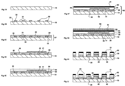
[0072] Figs. 1A-6J are diagrammatic cross-sections of stages in the
manufacture and
conversion of assemblies according to various embodiments of the present
invention.
[0073] Figs. 7 and 8 are diagrammatic cross-sections through methods of
removing
unwanted marking material according to various embodiments of the present
invention.
[0074] Figs. 9A and B are diagrammatic cross-sections through an ink fracture
mechanism according to various embodiments of the present invention.
[0075] Figs. 10A - 13B are elevations of finished vision control panels
according to
various embodiments of the present invention.
DETAILED DESCRIPTION OF PREFERRED
EMBODIMENTS OF THE INVENTION
[0076] Figs. lA-J are diagrainmatic cross-sections through the manufacture of
an
assembly, shown in Fig. l C, and its subsequent conversion to form a one-way
vision
control panel, in Figs.1D-J. Fig.lA illustrates substrate 10 and Fig.1B shows
stencil
layer 20 coinprising release surface 22 adj acent to the substrate and/or
release surface
23 remote from the substrate. Stencil layer 20 defines a print pattern 21
which is
devoid of the stencil layer. In Fig. 1C, partially adhered transparent coating
30 is
applied to both the substrate throughout the print pattern 21 and the stencil
layer 20, in
one continuous coating or a plurality of coatings, to form an assembly
according to
26
CA 02669540 2009-05-13
WO 2008/084332 PCT/IB2007/004462
one or more embodiments of the invention, typically a Part Processed Material
to be
converted to fonn a finished panel with a plurality of layers of marking
material in
substantially exact registration. Partially adhered transparent coating 30 is
typically
transparent. In Fig. 1D, design layer 40 comprises design color layer 41 of a
single or
"spot" color, the design printed reverse-reading, to be visible right-reading
through
partially adhered transparent coating 30 and substrate 10. Fig. 1E shows
background
color layer 50, for example a layer of white ink to act as a background to
design 40.
Another background color layer 51, for example a layer of black inlc, is
applied to
background color layer 50 in Fig. 1F. In Fig.1F, superimposed layers of
marking
material 49 comprise design layer 40, background color layer 50 and another
background color layer 51. In order to produce the finished panel, unwanted
layers of
marlcing material outside the print pattern are removed, typically by the
application of
a force at the exposed surface of the background color layer or layers remote
from the
substrate, for example by the application and removal of an adhering layer,
for
example a layer of plastisol inlc or a self-adhesive film 60, comprising a
filmic layer
62, for exainple of plastic or paper and pressure-sensitive adhesive 61, as
illustrated in
Fig. 1 G. Upon removal of the adhering layer, t11e unwanted ink is removed,
either
with the stencil layer as illustrated in Fig. 1 H if the stencil release layer
is adjacent to
substrate 10, or retaining the stencil layer 20 on the substrate, if the
stencil release
layer 23 is reinote from the substrate, as illustrated in Fig. 1J.
A1tenlatively, the
unwanted inlc may be removed by abrasion, for exainple by high-pressure water
j etting, witll or without an abrading medium, or air j etting with or without
an abrading
medium. In the case of a one-way vision panel, the stencil layer 20 in Fig. 1J
should
be transparent, in order to allow through vision from the printed side of
substrate 10,
27
CA 02669540 2009-05-13
WO 2008/084332 PCT/IB2007/004462
while design 40 is visible through substrate 10 and partially adhered
transparent
coating 30. Example materials for use with the embodiment of Figs 1 A-J
include a
plastic substrate, for example clear, transparent acrylic, pvc, polycarbonate
or print-
treated polyester, for example print-treated with a coating or co-extruded
layer to be
receptive to the adhesion of partially adhered transparent coating 30. Stencil
20 can
be of any material which can be accurately printed to define the print pattern
and
which does not adhere well to substrate 10 and/or subsequently applied layers
of
marlcing material, for exainple an organic solvent-based printing ink with low
adhesion to the particular substrate or the subsequently applied layers of
marking
material which comprise, for example, a conventional pvc solvent-based ink
with.
good adhesion to the particular substrate and each successive layer, for
exainple
Coates Vynaglaze. In this embodiment, the partially adhered transparent
coating can
be the clear ink within the Coates Vynaglaze range of inks, sometimes referred
to as a
vaillish ii-Ac, which adheres well to the substrate referred to above and the
superimposed layers of marking material, having compatible ink resin and
solvents.
Typically, the Part Processed Material assembly of Fig. 1C is sufficiently
durable to
be cut, packaged and shipped to printers, whether in sheet or roll form, to be
handled
by the printer and managed through an imaging system, typically a printing
machine,
without damaging the stencil layer 20.
[0077] Figs. 2A-F are similar to Figs. 1D-J, except that the Part Processed
Material of
Fig. 1 C is printed with a design layer 40 coinprising a layer of four color
process inks
42, for example typically applied in the order of process black (K), yellow
(Y)
magenta (M), and cyan (C), the design being printed reverse-reading but to be
visible
riglit-reading tluough partially adhered transparent coating 30 and substrate
10.
28
CA 02669540 2009-05-13
WO 2008/084332 PCT/IB2007/004462
Suitable four color process inks include, for example, Coates Vynaglaze cyan,
magenta, yellow and process black for screen printing or solvent inkjet inks
supplied,
for exainple, by HP Scitex, a division of Hewlett Packard, US.
[0078] Figs. 3A-G illustrate the second embodiment of the invention in which
the
assembly of Fig. 3A is similar to the assembly of Fig. 2C but with an
additional print-
receptive layer 70, for example a coating receptive to water-based inkjet inks
known
in the art, for exainple silicate-based or polymeric pvp or pva ("swellable")
ink-
receptive layers. The print-receptive layer is advailtageously applied to a
solvent-
resistant layer, for example a polyurethane varnish. The four color process
inks 42 of
design 40 in Fig. 3B, for example water-based inks supplied by Hewlett
Packard,.
adhere well to the print-receptive layer 70. Figs. 3 C - G illustrate similar
production
stages to Figs. 2B - F. A print-receptive layer of Coates Vynalam transparent
medium 269506 is receptive to most imaging systems designed to print on PVC
film,
for example, solvent inkj et.
[0079] Figs. 4A-F illustrate the production of a see-tllrough graphic panel
according
to US RE37,186 comprising reverse-printed design layer 42 visible through
partially
adhered transparent coating 30 and substrate 10, and right-reading design
layer 43, for
exaiuple a four color process layer printed in the order CMYK aild visible
from the
printed side of substrate 10. The intermediate layers between design layers 42
and 43
typically coinprise a plurality of white background color layers 50 and,
optionallyl a
layer 52 intermediate two white background color layers 50, for example a
silver,
gray, black or a partially printed black layer, for exainple a 50% coverage of
process
black ii12c.
29
CA 02669540 2009-05-13
WO 2008/084332 PCT/IB2007/004462
[0080] Figs. 5A-H illustrate diagrammatic cross-sections in the stages of
production
of a see-through graphic panel according to US 6,212,805 comprising a
translucent
design layer 41 in Fig. 5D, and translucent background color layer 58,
typically white,
in Fig. 5E. The finished panel of Fig. 5G with the stencil reinoved or of Fig.
5H with
the stencil retained can be illuminated from the printed side of substrate 10
and the
design will be clearly visible during the hours of darkness from the other
side of
substrate 10. Figs. 5J-M ilhistrate the production of a see-tlirough graphic
panel
according to US 6,212,805 coinprising two design layers 40 both facing in the
same
direction, eitlier both printed reverse-reading or both printed right-reading,
disposed
on either side of intermediate translucent background color layer 58,
typically white.
Fig. 5L is the finished panel if the stenci120 is removed and Fig. 5M is the
finished
panel if the stenci120 is retained.
[0081] Figs. 6A-E are similar to Figs 5D-H and Figs. 6F-J are similar to
Figs.5J-M,
except that design layer 40 comprises four color process design layer 42
printed
reverse-reading, typically in the order of KYMC.
[0082] Fig 7 is a cross-section tlirougli part of a machine for the automatic
lainination
and delamination of self-adhesive material 60 to imaged assembly 48
coinprising the
superiinposed layers 49 of partially adhered transparent coating and marking
material,
stencil layer 20 and substrate 10 by means of nip rollers 80, which are
optionally
heated. When the self-adhesive material is pulled away froin the imaged
assenibly,
unwanted superimposed layers 49 and stencil layer 20 are selectively removed
in
unwanted material portions 65 to a wind-up spool (not shown) for subsequent
disposal, leaving the desired superiinposed layers in the desired printed
portions 59 of
the print pattern in substantially exact registration.
CA 02669540 2009-05-13
WO 2008/084332 PCT/IB2007/004462
[0083] Fig. 8 is similar to Fig. 7 except that supplementary nip rollers 81
enhance the
bond between the self-adhesive assembly 60 and the imaged assembly 48 prior to
de-
lamination, feeding of the finished panel being assisted by feed rollers 82.
[0084] Fig. 9A is a diagrammatic cross-section through a portion of stencil
layer 20
on substrate 10 with superimposed, partially adhered transparent coating 30,
design
layer 40, baclcground color layer 50, for example of white ink, and another
background layer 51, for exa.inple of black iiik, subjected to ink removal
force 95, for
example by meaiis of the lainination and de-lamination of a self-adhesive film
(not
shown), causing ink fracture mechanism 90, resulting in the removal of
unwanted
material portion 65, for example as illustrated in Fig. 9B.
[0085] Figs. l0A and l OB illustrate elevations of the panel of Fig. 1H. In
Fig. 10A
design 40 "ABCD" is visible tllrough optically transparent substrate 10 and
transparent coating 30 against a white background color layer 50 in a print
pattern of
lines. Fig. l OB illustrates the other, printed side of the panel, black lines
51 permitting
good visibility through the optically transparent substrate 10 in between
black lines
51.
[0086] Figs. 11A and 11B illustrate elevations of the panel of Fig. 5G. In
Fig. 1 lA
design 40 "ABCD" is visible through optically transparent substrate 10 and
transparent coating 30 against a white background color layer 50 in a print
pattern of
lines. Fig. 11B illustrates the otlzer, printed side of the panel, the reverse
image of
design 40 being visible through translucent white lines 50, pennitting soine
visibility
through the optically transparent substrate 10 and transparent coating 30 in
between
white lines 50.
31
CA 02669540 2009-05-13
WO 2008/084332 PCT/IB2007/004462
[0087] Figs. 12A and 12B illustrate elevations of the panel of Fig. 4E. In
Fig. 12A , a
four color process design 42 "ABCD" is visible througli optically transparent
substrate
and transparent coating 30 against a white background color layer 50 in a
print
pattern of lines. Fig. 12B illustrates the other, printed side of the panel,
another four
color process design 43 being visible against a white background color layer
50 in the
print pattern of lines, permitting some visibility through the optically
transparent
substrate 10 in between white lines 50.
[0088] Figs. 13A aild 13B illustrate elevations of the pailel of Fig. 5L. In
Fig. 12A,
design 40 "ABCD" is visible through optically transparent substrate 10 and
transparent coating 30 against a white background color layer 50 in a print
pattern of
lines. Fig. 13B illustrates the other, printed side of the panel, the reverse
of design 40
being visible against the white background color layer 50 in the print pattern
of lines,
permitting good visibility through the optically transparent substrate 10 in
between
white lines 50.
[0089] One or inore embodiments of the invention are capable of being
practiced by a
wide range of partially adhered transparent coating materials and imaging
systems,
providing these are compatible, including the requirement that all layers of
the
partially adllered transparent coating and subsequently applied marking
materials or
colorants inust adhere to each adjacent layer. The partially adhered
transparent
coating optionally coinprises proprietary materials foi7nulated and used for
otlier
purposes or only a single one purpose of the inultiple purposes of the
partially adhered
transparent coating. For example, "Lyson Printbond" supplied by Nazdar, Inc.,
US,
adheres well to a wide variety of substrates and provides an excellent print-
receptive
surface for virtually all solvent and UV imaging systems. However, it also
provides
32
CA 02669540 2009-05-13
WO 2008/084332 PCT/IB2007/004462
the ability to hold down the stencil layer and, as a halogenated polyolethene,
is hard to
dissolve and thus provides a protection to the stencil layer and substrate
from inlc
solvents.
[0090] As another example, of the second embodiment, a printer can apply
"Lyson
Pre-Post" coating, made by Nazdar, Inc., USA, within approximately one hour of
printing, when it will absorb water-based inks but then becomes water-
resistant, a
common requirement of vision control panels made by one or more embodiments of
the present invention.
[0091] The foregoing illustrated embodiments are provided to illustrate the
structural
and functioilal principles of the present invention and are not intended to be
limiting.
To the contrary, the principles of the present invention are intended to
encoinpass any
and all changes, alterations and/or substitutions within the spirit and scope
of the
following claims.
33