Note: Descriptions are shown in the official language in which they were submitted.
CA 02669679 2009-05-13
WO 2008/062971 PCT/KR2007/005779
-1-
METHOD AND APPARATUS FOR RECEIVING SYSTEM
INFORMATION FROM BASE STATION IN A MOBILE
COMMUNICATION SYSTEM
BACKGROUND OF THE INVENTION
1. Field of the Invention
The present invention relates generally to a mobile communication system,
and more particularly, to a method and apparatus for receiving system
information
from a Base Station (BS) in a Mobile Station (MS) in a mobile communication
system.
2. Description of the Related Art
In a mobile communication system, a BS transmits to an MS system
information, which refers to various pieces of information required for
communications between the BS and the MS, including information for channel
establishment and a list of neighbor cells. The system information is carried
in
System Information Blocks (SIBs), generally 18 SIBs.
The BS can use one of two methods to notify the MS of a change in the
system information, i.e. a change in the SIBs. In one of the methods, the BS
periodically transmits a Master Information Block (MIB) and the MS monitors
the MIB. The MIB transmission period is equal to the monitoring period. The
MIB, which provides information required for transmission of the SIBs,
includes
infonnation bits called an MIB value tag and SIB value tags. The MIB value tag
indicates whether the system information has been changed and the SIB value
tags indicate an SIB that has been changed.
The MIB or the SIBs can be broadcast on a Broadcast Control CHannel
(BCCH).
In this method, the MS monitors the system information in the same
period as the transmission period of the system information of the BS.
Therefore,
when the system infonnation is changed, modification time information is not
needed. The modification time information indicates a time when the changed
CA 02669679 2009-05-13
WO 2008/062971 PCT/KR2007/005779
-2-
system information is applied.
The other method is that the BS notifies the MS of a change in the system
information when the change occurs, rather than periodically. This method
requires the modification time information.
A brief description will now be made of how it is determined whether the
system information has been changed by use of the value tags. The following
description applies to both the methods.
If a first MIB value tag is 0 and a second MIB value tag is 0, this indicates
that no change has occurred to the system information. If an SIB is changed,
the
MIB value tag is set to 1, to thereby notify the MS of a change in the system
information. Each time the system information changes, the MIB value tag
sequentially increases. The MIB value tag just notifies the MS of whether the
system information has been changed, and does not indicate the changed system
information. Hence, when receiving a different MIB value tag compared to the
previous one, the MS identifies the changed system information by checking SIB
value tags.
If the MIB value tag is changed to 1 in the above example, the MS
determines that the system information has been changed. To find out the
changed
system information, the MS then reads each of the 18 SIB value tags and
acquires
the changed system information from an SIB corresponding to a changed SIB
value tag.
FIG 1 illustrates a signal flow for a conventional operation for receiving
system information from an Evolved Radio Access Network (E-RAN) in a User
Equipment (UE) in a mobile communication system.
Referring to FIG 1, in the mobile communication system, an E-RAN 100
transmits an MIB with an MIB value tag to a UE 110 in step 120 and an SIB to
the UE 110 in step 130. It is assumed that the MIB value tag is error-free and
has
an increased value and thus the UE 110 has read SIB value tags. To determine a
changed SIB using a changed SIB value tag, the UE 110 checks an error in the
CA 02669679 2009-05-13
WO 2008/062971 PCT/KR2007/005779
-3-
received SIB in step 140. If the SIB has an error, the UE 110 neglects the SIB
in
step 150 and receives a new SIB in step 160. For the sake of 'convenience, a
description of MIB transmission is not provided herein.
In step 170, the UE 110 checks errors in the SIB. If no errors are detected,
the UE 110 buffers the SIB in a buffer in step 180. If an error is detected in
the
received SIB, the UE 110 neglects the SIB and repeats SIB reception until no
errors are detected in the procedure of FIG. 1. The repetition causes a long
time
delay for the UE to receive normal SIBs and determine the changed system
information. As a consequence, communications are delayed between the E-RAN
and the UE.
SUMMARY OF THE INVENTION
An aspect of the present invention is to address at least the problems
and/or disadvantages and to provide at least the advantages described below.
Accordingly, an aspect of the present invention is to provide a method and
apparatus for receiving system information without errors in a UE.
Another aspect of the present invention is to provide a method and
apparatus for increasing the reception rate of system information in a UE.
A further aspect of the present invention is to provide a method and
apparatus for reducing the time delay of receiving system information in a UE.
In accordance with the present invention, there is provided a method for
receiving system information from a BS in an MS in a mobile communication
system, in which it is determined whether there is buffered system information
in
a buffer, if current system information has an error, it is determined whether
a
combining condition is satisfied, in the presence of the buffered system
information, the combining condition being defined by at least one of an MIB
value tag, an SIB value tag, and modification time information that are
associated
with the current system information, and the current system information is
combined with the buffered system information, if the combining condition is
satisfied.
CA 02669679 2009-05-13
WO 2008/062971 PCT/KR2007/005779
-4-
In accordance with the present invention, there is provided an apparatus
for receiving system information from a BS in an MS in a mobile communication
system, in which a receiver receives system information and at least one of an
1VIIB value tag, an SIB value tag, and modification time information that are
associated with the system information, an error checker checks errors in the
received system information and outputs an error check result, a controller
provides the system information to one of a buffer and a combiner according to
whether a combining condition or a buffering condition is satisfied based on
the
error check result, the combining condition and the buffering condition being
defined by at least one of the MIB value tag, the SIB value tag, and the
modification time information, the buffer buffers the system information
received
from the controller, if the buffering condition is satisfied, and the combiner
combines system information buffered in the buffer with the system information
received from the controller, if the combining condition is satisfied.
BRIEF DESCRIPTION OF THE DRAWINGS
The above and other objects, features and advantages of preferred
embodiments of the present invention will be more apparent from the following
detailed description taken in conjunction with the accompanying drawings, in
which:
FIG 1 illustrates a signal flow for a conventional operation for receiving
system information from an E-RAN in a UE in a mobile communication system;
FIG. 2 illustrates the configuration of a mobile communication system
according to the present invention;
FIG 3 illustrates a UE for receiving an SIB according to the present
invention;
FIG 4 illustrates a signal flow for an operation for receiving an SIB in the
UE according to the present invention;
FIG 5 illustrates an operation for receiving an SIB in the UE according to
a first embodiment of the present invention;
FIG 6 illustrates an operation for receiving an SIB in the UE according to
a second embodiment of the present invention;
FIG 7 illustrates an operation for receiving an SIB in the UE according to
a third embodiment of the present invention;
CA 02669679 2009-05-13
WO 2008/062971 PCT/KR2007/005779
-5-
FIG. 8 illustrates a signal flow for an operation for receiving an SIB earlier
than an SIB value tag in the UE according to the present invention;
FIG. 9 illustrates an operation for receiving an SIB in the UE according to
a fourth embodiment of the present invention; and
FIG. 10 illustrates an operation for receiving an SIB in the UE according
to a fifth embodiment of the present invention.
Throughout the drawings, the same drawing reference numerals will be
understood to refer to the same elements, features and structures.
DETAILED DESCRIPTION OF THE PREFERRED EMBODIMENTS
The matters defined in the description such as a detailed construction and
elements are provided to assist in a comprehensive understanding of preferred
embodiments of the invention. Accordingly, those of ordinary skill in the art
will
recognize that various changes and modifications of the embodiments described
herein can be made without departing from the scope and spirit of the
invention.
Also, descriptions of well-known functions and constructions are omitted for
the
sake of clarity and conciseness.
The present invention increases the reception success rate of SIBs by
combining a previously stored SIB with a received SIB according to a combining
condition that is defined by an MIB value tag, a modification time and an SIB
value tag. Compared to the conventional technology, SIB value tags can be
transmitted together with an MIB value tag or separately from the MIB value
tag
in the present invention. As previously described, one of the two methods for
receiving system information in the UE requires the modification time
information, whereas the other method does not require the modification time
information. The present invention is applicable to the two cases.
FIG 2 illustrates a mobile communication system according to the present
invention.
Referring to FIG 2, an E-RAN 215 is configured in a simple structure
having Evolved Node Bs (ENBs) 225, 230, 235, 240 and 245 and anchor nodes
CA 02669679 2009-05-13
WO 2008/062971 PCT/KR2007/005779
-6-
205 and 210. A UE 250 accesses an Internet Protocol (IP) network via the E-RAN
215. The ENBs 225 to 245 are connected wirelessly to the UE 250. Since all
user
traffic including real-time services such as Voice over IP (VoIP) is serviced
on a
shared channel, the ENBs 225 to 245 collect the status information of UEs and
schedule them, for reliable information transmission/reception.
Typically, one ENB controls a plurality of cells. The ENB performs
Adaptive Modulating and Coding (AMC) that determines a modulation scheme
and a channel coding rate for a UE adaptively according to the channel status
of
the UE. Hybrid Automatic Repeat reQuest (HARQ) is carried out between the
ENBs 225 to 245 and the LTE 250. Because HARQ alone has limitations in
satisfying different Quality of Service (QoS) requirements, an outer ARQ is
performed between the UE 250 and the ENBs 225 to 245 in an upper layer.
HARQ increases a reception success rate by soft-combining previous
received data with retransmitted data without discarding the previous received
data. HARQ is adopted to achieve high transmission efficiency in high-speed
packet cominunications such as High Speed Downlink Packet Access (HSDPA)
and Enhanced Dedicated CHannel (EDCH).
FIG 3 illustrates a UE for receiving SIBs according to the present
invention.
Referring to FIG. 3, a receiver 300 receives an SIB from the ENB 230. An
error checker 310 checks errors in the received SIB by, for exainple, a Cyclic
Redundancy Check (CRC). A controller 320 provides the SIB to a buffer 330 or a
combiner 340 according to a condition defined by an MIB value tag, an SIB
value
tag, and a modification time that are associated with the SIB. The condition
will
be detailed later herein.
The buffer 330 buffers the received SIB or a combined SIB and provides a
buffered SIB to the combiner 340 and the received SIB or the combined SIB to a
decoder 350 according to commands received from the controller 320. The
combiner 340 combines the received SIB with the buffered SIB and provides the
combined SIB to the buffer 330. The decoder 350 decodes the received SIB
CA 02669679 2009-05-13
WO 2008/062971 PCT/KR2007/005779
-7-
without errors or the combined SIB and provides the decoded SIB to the
controller 320.
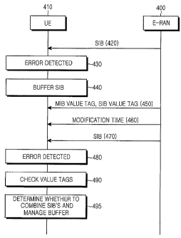
FIG 4 illustrates a signal flow for an operation for receiving an SIB in the
UE according to the present invention.
Referring to FIG 4, on the assumption that a UE 410 has received a
changed MIB value tag and thus checked SIB value tags, the UE 410 receives an
SIB from an E-RAN 400 in step 420. Since the MIB value tag has an increased
value, the UE 410 should acquire changed system information from an SIB
corresponding to a changed SIB value tag. Hence, the UE 410 checks errors in
the
received SIB in step 430. If the SIB has an error, the UE 410 buffers the SIB
in
the buffer 330 in step 440. This SIB is referred to as a buffered SIB. The UE
410
also stores the MIB value tag and the SIB value tags in the buffer 330 or any
other storage (not shown). In step 450, the UE 410 receives an MIB value tag
and
SIB value tags at the next scheduling time. It is assumed that the UE 410
receives
modification time information in step 460.
In step 470, the UE 410 receives an SIB. While the MIB value tag, the
SIB value tags and the modification time information are received in separate
steps, they can be received together. The UE 410 performs an error check on
the
received SIB in step 480. If the SIB has an error, the UE 410 compares at
least
one of the stored MIB value tag and SIB value tags with the received MIB value
tag, SIB value tags, and modification time information. The UE 410 determines
whether to combine or buffer the received SIB according to a combining
condition after the coinparison in step 495. The combining condition is
defined
according to whether the received MIB value tag has been changed, the received
SIB value tags have been changed, and the UE receives the modification time
information.
For better understanding of the present invention, the preferred
embodiments of the present invention are classified according to the following
two criteria.
(1) The preferred embodiments of the present invention are divided
depending on whether the UE receives modification time information. The
CA 02669679 2009-05-13
WO 2008/062971 PCT/KR2007/005779
-8-
instance when the UE does not receive modification time information will be
described with reference to FIGs. 5, 6 and 9. The instance when the UE
receives
modification time information will be described with reference to FIGs. 7 and
10.
(2) The preferred embodiments of the present invention are divided
depending on whether the UE receives an SIB earlier than an SIB value tag. The
instance when the UE receives an SIB later than an SIB value tag will be
described with reference to FIGs. 5, 6 and 7. The instance when the UE
receives
an SIB earlier than an SIB value tag will be described with reference to FIGs.
9
and 10.
Unlike the conventional technology, the UE can receive an SIB earlier
than an SIB value tag in the present invention. The present invention is not
limited to the instance when an SIB value tag is transmitted together with an
MIB
value tag in an MIB. That is, the SIB value tag can be transmitted separately
from
the MIB value tag depending on system configuration.
FIGs. 5, 6 and 7 illustrate preferred embodiments of the present invention
in which the UE receives an SIB according to a combining condition.
FIG 5 illustrates an operation for receiving an SIB in the UE according to
a first embodiment of the present invention.
Combining condition 1 for the procedure of FIG. 5 is that when the UE
does not receive modification time information, the latest received MIB value
tag
(i.e., a current MIB value tag) has the same value as a stored MIB value tag
(i.e.,
a buffered MIB value tag). Since the MIB value tag has not been changed,
current
SIB value tags are identical to buffered SIB value tags. Therefore, the
combining
condition does not involve the SIB value tags.
Referring to FIG 5, the UE receives a current SIB in step 500 and checks
for errors in the current SIB in step 510. When the current SIB has an error,
the
UE proceeds to step 520 and if the current SIB has no errors, the UE juinps to
step 570.
CA 02669679 2009-05-13
WO 2008/062971 PCT/KR2007/005779
-9-
Since the current SIB is error-free, it can be applied to the UE
iminediately in step 570. Hence, the current SIB is directly output, without
being
buffered in the buffer.
In step 520, the UE determines whether there is a buffered SIB in the
buffer. In the absence of a buffered SIB, the UE buffers the current SIB in
the
buffer because the current SIB is the latest SIB in step 560.
In the presence of a buffered SIB, the UE combines the buffered SIB with
the current SIB in step 530 and checks for errors in the combined SIB in step
540.
If the combined SIB has no errors, the UE outputs the combined SIB without
buffering it in step 570. If the combined SIB has an error, the UE clears the
buffer
in step 550 and buffers the combined SIB in the buffer in step 580.
FIG 6 illustrates an operation for receiving an SIB in the UE according to
a second embodiment of the present invention.
Combining condition 2 for the procedure of FIG 6 is that when the UE
does not receive modification time information, a current MIB value tag has a
different value from that of a buffered MIB value tag and a current SIB value
tag
has the same value as a buffered SIB value tag.
Referring to FIG 6, the LTE receives a current SIB in step 600 and checks
for errors in the current SIB in step 605. When the current SIB has an error,
the
UE proceeds to step 610 and if the current SIB has no errors, the UE jumps to
step 650.
Since the current SIB is error-free, it can be applied to the UE
immediately in step 650. Hence, the current SIB is directly output, without
being
buffered in the buffer.
In step 610, the UE determines whether there is a buffered SIB in the
buffer. In the absence of a buffered SIB, the UE buffers the current SIB in
the
buffer because the current SIB is the latest SIB in step 655.
CA 02669679 2009-05-13
WO 2008/062971 PCT/KR2007/005779
-10-
In the presence of a buffer SIB, the UE compares a current SIB value tag
with a buffered SIB value tag in step 615. If the two SIB value tags are
different,
the UE clears the buffered SIB from the buffer in step 620 and buffers the
current
SIB in the buffer since the current SIB is the latest SIB in step 625.
If the two SIB value tags are identical, the UE combines the current SIB
with the buffered SIB in step 630 and checks for errors in the combined SIB in
step 635. If no errors are detected from the combined SIB, the UE outputs the
combined SIB without buffering it in step 650. If an error is detected in the
combined SIB, the UE clears the buffered SIB from the buffer in step 640 and
buffers the combined SIB in step 645.
FIG. 7 illustrates an operation for receiving an SIB in the UE according to
a third exemplary embodiment of the present invention.
Colnbining condition 3 for the procedure of FIG 7 is that when the UE
receives modification time information, a current 1VIIB value tag has a
different
value from that of a buffered MIB value tag, a buffered SIB is received after
a
modification time, and a current SIB value tag has the same value as a
buffered
SIB value tag.
Referring to FIG. 7, the UE receives a current SIB in step 700 and checks
for errors in the current SIB in step 705. When the current SIB has an error,
the
UE proceeds to step 710 and if the current SIB has no errors, the UE jumps to
step 755.
Since the current SIB is error-free, it can be applied to the UE immediately.
Hence, the current SIB is directly output, without being buffered in the
buffer in
step 755.
In step 710, the UE determines whether there is a buffered SIB in the
buffer. In the presence of a buffered SIB, the UE proceeds to step 715 and in
the
absence of a buffered SIB, the UE proceeds to step 760. In step 760, since the
buffered SIB does not exist in the buffer or was received before the
modification
time, the UE buffers the current SIB being the latest SIB in the buffer. If
the
CA 02669679 2009-05-13
WO 2008/062971 PCT/KR2007/005779
-11-
current SIB has been received before the modification time information, this
indicates that the current SIB is not the latest SIB.
In step 715, the UE determines whether the buffered SIB was received
after the modification time. If the buffered SIB was received before the
modification time, the UE proceeds to step 760. If the buffered SIB was
received
after the modification time, the UE compares a current SIB value tag with a
buffered SIB value tag in step 720. If the two SIB value tags are different,
the UE
clears the buffered SIB from the buffer in step 725 and buffers the received
SIB in
the buffer since the current SIB is the latest SIB in step 730.
If the two SIB value tags are identical, the UE combines the current SIB
with the buffered SIB in step 735 and checks for errors in the combined SIB in
step 740. If no errors are detected from the combined SIB, the UE outputs the
combined SIB without buffering. it in step 755. If an error is detected in the
combined S`IB, the UE clears the buffered SIB from the buffer in step 745 and
buffers the combined SIB in step 750.
The embodiments depicted in FIGs. 5, 6 and 7 concern instances when the
UE receives an MIB value tag and an SIB value tag before receiving an SIB. As
previously stated, the UE can receive the SIB value tag separately from the
MIB
value tag. Hence, it may occur that the UE receives an SIB before the SIB
value
tag, which is illustrated in FIG. 8.
FIG 8 illustrates a signal flow for an operation for receiving an SIB earlier
than an SIB value tag in the UE according to the present invention.
Referring to FIG 8, a UE 810 receives a changed MIB value tag from an
E-RAN 800 and thus is aware of a change in an SIB in step 820. Thus, the UE
810 receives a new SIB in step 830 and receives an SIB value tag after the SIB
reception in step 840.
When an SIB value tag is transmitted separately from an MIB, the UE
may fail to receive the SIB value tag due to transmission loss, for example,
despite reception of an MIB value tag. FIGs. 9 and 10 describe the instance
when
CA 02669679 2009-05-13
WO 2008/062971 PCT/KR2007/005779
-12-
the UE fails to receive the SIB value tag.
FIG 9 illustrates an operation for receiving an SIB in the UE according to
a fourth embodiment of the present invention.
Combining condition 4 for the procedure of FIG 9 is that when the UE
does not receive modification time information, a current MIB value tag has a
different value from that of a buffered MIB value tag and a current SIB value
tag
has not been received.
Referring to FIG 9, the UE receives a current SIB in step 900 and checks
for errors in the current SIB in step 910. When the current SIB has an error,
the
UE proceeds to step 920 and if the current SIB has no errors, the UE jumps to
step 960.
Since the current SIB is error-free, it can be itnmediately applied to the
UE. Hence, the current SIB is directly output, without being buffered in the
buffer
in step 960.
In step 920, the UE determines whether there is a buffered SIB in the
buffer. In the presence of a buffered SIB, the UE proceeds to step 930 and in
the
absence of a buffered SIB, the UE proceeds to step 960. In step 960, since the
buffered SIB does not exist in the buffer, the UE buffers the current SIB
being the
latest SIB in the buffer.
In step 930, the UE combines the current SIB with the buffered SIB. The
UE checks for errors in the combined SIB in step 940. If no errors are
detected
from the combined SIB, the UE outputs the combined SIB without buffering it in
step 970. If an error is detected in the combined SIB, the UE clears the
buffered
SIB from the buffer in step 950 and buffers the current SIB in step 960. The
UE
does not buffer the combined SIB in step 960, because the UE cannot identify
an
SIB having changed system information among a plurality of SIBs if the UE has
not received the SIB value tag. Thus, when the combined SIB has an error, this
implies that the current SIB can be different from the buffered SIB. Thus, the
erroneous combined SIB is discarded and instead, the current SIB having the
CA 02669679 2009-05-13
WO 2008/062971 PCT/KR2007/005779
-13-
latest system information is buffered in the buffer.
FIG 10 illustrates an operation for receiving an SIB in the UE according
to a fifth embodiment of the present invention.
Coinbining condition 5 for the procedure of FIG 10 is that when the UE
receives modification time information, a current MIB value tag has a
different
value from that of a buffered MIB value tag and a buffered SIB was received
after
a modification time.
In FIG 10, the UE receives a changed MIB value tag and receives an SIB
value tag after receiving an SIB. As previously stated, the UE receives
modification time information.
Referring to FIG. 10, the UE receives a current SIB in step 1000 and
checks for errors in the current SIB in step 1010. When the current SIB has an
error, the UE proceeds to step 1020 and if the current SIB has no errors, the
UE
jumps to step 1080.
Since the current SIB is error-free, it can be immediately applied to the
UE. Hence, the current SIB is directly output, without being buffered in the
buffer
in step 1080.
In step 1020, the UE determines whether there is a buffered SIB in the
buffer. In the presence of a buffered SIB, the UE proceeds to step 1030 and in
the
absence of a buffered SIB, the UE goes to step 1090.
In step 1090, since the buffered SIB does not exist in the buffer or if any,
the buffered SIB was received before a modification time, the UE buffers the
current SIB being the latest SIB in the buffer.
In step 1040, the UE combines the current SIB with the buffered SIB. The
UE checks for errors in the combined SIB in step 1050. If no errors are
detected
from the combined SIB, the UE outputs the combined SIB without buffering it in
step 1080. If an error is detected in the combined SIB, the UE clears the
buffered
CA 02669679 2009-05-13
WO 2008/062971 PCT/KR2007/005779
-14-
SIB from the buffer in step 1060 and buffers the combined SIB in step 1070.
As is apparent from the above description, the present invention
advantageously increases the reception success rate of an SIB through
combining
in a UE, even though the SIB received from an ENB has an error in a mobile
communication system. Also, when the UE receives an SIB from an ENB, for
operation, the present invention decreases a reception time delay.
While the invention has been shown and described with reference to
certain exemplary embodiments of the present invention thereof, it will be
understood by those skilled in the art that various changes in form and
details
may be made therein without departing from the spirit and scope of the present
invention as defined by the appended claims and their equivalents.