Note: Descriptions are shown in the official language in which they were submitted.
CA 02670948 2009-05-28
English translation of PCT application
PCT/JP2007/072988
DESCRIPTION
PUMP PROBE MEASURING DEVICE AND SCANNING PROBE
MICROSCOPE APPARATUS USING THE DEVICE
Technical Field
[0001] The present invention relates to a pump probe measuring
device for measuring and analyzing ultrafast physical phenomena
and a scanning probe microscope apparatus using this measuring
device. More specifically, the invention relates to a pump probe
measuring device employing rectangular-wave-based delay time
modulation using pulse pickers, and a scanning probe microscope
apparatus using this measuring device.
Background Art
[0002] As the almost only means for measuring a phenomenon that
occurs in an extremely short time period of the order of picosecond
(ps) or femtosecond (fs), the pump probe method using an ultrashort
pulse laser beams is known. The pump probe method is available in
various embodiments. All the embodiments measure probe signals
as a function of delay time, which is the duration from the
excitation of a sample by pump light to the detection of the state of
the sample by probe light. Ultrafast response of the sample to
photoexcitation can thus be measured while achieving high time
resolution of the order of femtosecond.
[0003] Since the intensity of signals obtained by this measurement
method is low in general, modulation measurement is performed to
pick up desired signals from noise. The modulation of the pump
light intensity was the most common modulation measurement
method. This method has achieved good results in researches in
which time-resolved measurement is conducted to measure the
reflectance of probe light.
[0004] Depending on measurement environment, however,
modulation of high-intensity pump light causes the sample
temperature to increase and decrease repetitively, which may
1
CA 02670948 2009-05-28
English translation of PCT application
PCT/JP2007/072988
adversely affect the measurement. This problem has been a concern
in a series of researches to create a so-called time-resolved scanning
probe microscope capable of achieving ultimate resolution in both
time and space regions by combining the pump probe method and a
scanning probe microscope.
[0005] On the other hand, as a method that does not modulate light
intensity, the delay time modulation method is known. The
conventional delay time modulation method changes optical path
length by physically moving the position of a mirror placed on the
pump light path to adjust delay time. Consequently, with the delay
time modulation method, the limited capacity of a driving
mechanism for physically transferring the mirror restricts the
transfer distance of the mirror, causing delay time setting range to
be limited to 1 ns or shorter, and delay time modulation range to
100 Ps or shorter. In addition, since modulation cannot be realized
with a large-amplitude and high-frequency, modulation frequency is
limited to 20 Hz or lower, for example. Thus, the measurement of a
phenomenon having relaxation time of several hundred ps or longer,
for example, cannot be carried out. Furthermore, the mechanical
transfer of the mirror position vibrates an optical bench, causing the
optical axis to deviate and eventually decreasing measurement
accuracy.
[0006] Moreover, since the signal intensity is proportional to the
modulation amplitude in this delay time modulation method,
modulation amplitude must be increased to measure small and
gradual relaxation processes.
However, increasing modulation amplitude decreases
modulation frequency and thus increases noise amplitude. In
addition, since output signals are the average value over the entire
modulation amplitude, time resolution decreases. Furthermore,
since differentiated signals are measured with this delay time
modulation method in principle, the absolute value of signals cannot
be found, which makes physical interpretation difficult.
Meanwhile, taking advantage of the feature that it does not
cause increase and decrease of the temperature of samples and the
2
CA 02670948 2009-05-28
English translation of PCT application
PCT/JP2007/072988
measurement system, this conventipnal delay time modulation
method was combined with a scanning probe microscope into a
delay-time-modulated scanning probe microscope, which has
accomplished certain results.
[0007] On the other hand, a new delay time modulation method was
designed recently. It has two laser oscillators oscillating at
repetition frequencies slightly differing from each other and are
used for each laser as a pump light and a probe light. In this case,
the delay time is scanned from zero to the repetition period at high
speed at the modulation frequency equivalent to the difference
between the two repetition frequencies. By recording probe signals
in synchronization with the frequency equivalent to the difference
between the above repetitive frequencies and averaging the obtained
values, the measurement can be performed easily even in a large
delay time region without mechanically changing the mirror
position, and the absolute signal values can thus be measured.
Furthermore, this method is superior to the previously mentioned
methods in that modulation frequency can be increased.
[0008] Nonpatent literature 1: A. Bartels, Appl. Phys. Lett. 88,
041117 (2006)
Disclosure of the Invention
Problems to be Solved by the Invention
[00091 However, in order to take advantage of this new delay time
modulation method, a probe signal detector with relatively wide
bandwidth is required. If the bandwidth of the probe signal detector
is narrow, the modulation frequency, which is the difference between
the repetitive frequencies of two lasers, must be decreased to
extremely low level. This increases noise level. In addition, since
this new delay time modulation method requires two expensive laser
oscillators, which must be oscillated synchronized, the overall cost
of the measurement apparatus increases.
[0010] Under such circumstances, an inexpensive pump probe
measuring device featuring wide measurement range and high
detection sensitivity, and applicable to special measurement
3
CA 02670948 2009-05-28
English translation of PCT application
PCT/JP2007/072988
environment including combined use with a scanning probe
microscope, has been much sought after.
[0011] The object of the present invention is to solve the above
problems in time-resolved measurement using pulse lasers
applicable to the femtosecond region, by providing a pump probe
measurement device for measuring ultrafast physical phenomena for
analyses capable of measuring faint signals stably and highly
accurately over a wide measurement range, including phenomena
having short or long relaxation time, without modulating the
intensity of irradiated light, namely without being affected by heat,
and a time-resolved scanning probe microscope apparatus using that
device.
Means for Solving the Problem
[0012] To achieve the above object, the present invention provides a
pump probe measuring device including: an ultrashort optical pulse
laser generator for generating a first ultrashort optical pulse train,
which becomes a pump light, and a second ultrashort optical pulse
train, which becomes a probe light; a delay time adjusting unit for
adjusting a delay time of the first and the second ultrashort optical
pulse trains; a first pulse picker and a second pulse picker for
reducing effective repetition frequency of optical pulses by accepting
each of the first and second ultrashort optical pulse trains and
transmitting only one pulse at an arbitrary repetition frequency; a
delay time modulating unit for periodically changing a position
through which optical pulses are transmitted by the first and the
second pulse pickers; a measuring unit for detecting probe signals
from a sample equipped with an irradiation optical system for
applying the pump light and probe light to the sample; and a lock-in
detecting unit for performing phase-sensitive detection of probe
signals from the sample at a modulation frequency of the delay time
modulation unit, wherein the first or the second pulse picker
changes the position through which optical pulses are transmitted,
thus changing the delay time between the optical pulse that is
transmitted through said second pulse picker and the optical pulse
4
CA 02670948 2009-05-28
English translation of PCT application
PCT/JP2007/072988
that is transmitted through said first pulse picker.
According to the above configuration, by periodically
changing the timing at which the pulse picker transmits and blocks
the pump light and the probe light pulses, which are continuously
generated by the ultrashort optical pulse laser generator, the delay
time can be changed by large amount at high speed.
[0013] Since the present invention does not employ modulation of
pump light intensity, repetitive temperature change does not occur;
even samples sensitive to temperature change during measurement
are not affected adversely. Samples in a broad range of fields can
thus be measured.
[0014] According to the present invention, by transmitting and
blocking optical pulses generated from laser equipment using pulse
pickers in order to transmit optical pulses at relatively long
repetition period, a physical phenomenon having relaxation time
longer than the repetition period of the laser equipment, 1 I.AS for
example, can be measured easily. Since measurement can be made
even in a very large delay time region, exceeding the optical pulse
repetition frequency, a probe signal in excited state and that after
complete relaxation of the sample can be compared. As a result, not
only the differential value but also the absolute value of the signal
can be obtained, which facilitates physical interpretation.
Furthermore, since there is no need to shift the mirror position over
a long distance, the optical axis of output laser beams does not
deviate, thus ensuring high measurement accuracy.
[0015] According to the present invention, since the modulation
amplitude can be increased, the signal intensity increases to several
to several tens times that of the conventional delay time modulation
method. In addition, a high modulation frequency allowed in the
present invention decreases the noise intensity down by half to
approximately one tenth of the conventional method, for example,
when a long relaxation period of several picoseconds or longer is
measured. This allows the so-called signal-to-noise (SIN) ratio to be
increased by approximately 50 to 100 times that of the conventional
method.
CA 02670948 2009-05-28
English translation of PCT application
PCT/JP2007/072988
[00161 In the above configuration, the pulse pickers preferably
include Pockels cells and light polarizers to transmit and block
arbitrary optical pulses. The delay time modulation unit preferably
includes: a photosensor for detecting optical pulses generated by the
ultrashort optical pulse laser generator; a counting means for
counting pulse signals from the photosensor; a delaying means to be
connected to the counting means; and a driving means for the pulse
pickers. According to this configuration, arbitrary pulses can be
transmitted or blocked quite easily.
[0017] In the above configuration, the ultrashort optical pulse laser
generator can include a laser source comprising a titanium-sapphire
laser oscillator. In this configuration, since laser pulses having, for
example, wavelength of 800 nm and pulse width of 25 fs can be
generated at the repetition frequency of approximately 100 MHz,
ultrashort optical pulse laser can be obtained easily.
[00181 If the delay time adjusting unit includes an optical system
that adjusts optical path length using movable mirrors, delay time
can be adjusted using a delay time adjusting unit similar to a
conventional one. In addition, since the mirror need not be
transferred over a long distance, the optical axis of the pulse light
applied to a sample rarely deviates, and as a result measurement
accuracy increases.
[0019] If the ultrashort optical pulse laser generator includes an
ultrashort optical pulse laser source and an optical device that
divides the ultrashort optical pulses generated by the ultrashort
optical pulse laser source into two optical paths to form pump light
and probe light, only one ultrashort optical pulse laser device is
needed as a light source, which ensures simple configuration and
reduces overall device cost.
[0020] In a configuration in which the ultrashort optical pulse laser
generator is equipped with two ultrashort optical pulse laser
sources that emit light in the same cycles, and the ultrashort optical
pulses generated at each ultrashort optical laser source are made to
enter corresponding pulse pickers as the pump light and the probe
light respectively, there is no need to branch light in order to feed it
6
CA 02670948 2009-05-28
English translation of PCT application
PCT/JP2007/072988
to two pulse pickers. Consequently, the intensity of the optical pulse
applied to the sample can be enhanced, and the phase of the pump
light and probe light can be shifted easily. If the two ultrashort
optical pulse laser sources have different wavelengths, the pump
light and the probe light can be made to have different wavelengths.
Furthermore, if a synchronous oscillation control mechanism is
provided for the two laser devices, by setting the phase of oscillating
the pump light and probe light as required, the delay time up to the
repetition period can be set easily. Consequently, since delay time
can be adjusted by two ultrashort optical pulse laser sources and
=
pulse pickers, the delay time adjusting unit, which is required when
only one ultrashort optical pulse laser source is used, can be
omitted.
[0021] When a cavity dumper is used as an ultrashort optical pulse
laser source, by decreasing the repetition frequency of the optical
pulses coming from the ultrashort optical pulse laser source, the
intensity of each optical pulse can be increased, which allows the
repetition frequency to be decreased without significantly
decreasing the average intensity. When the operating frequency of
the pulse pickers is limited to approximately 1 MHz, the optical
intensity of the pump light and the probe light can be increased.
[0022] The above measuring unit preferably includes an optical
system for irradiating the surface of the sample with the pump light
and the probe light, and another optical system for measuring the
intensity of reflected probe light, wherein the intensity of the
reflected probe light is output as probe signals. According to this
configuration, the change in reflectance on the surface of the
sample, which occurs when the surface of the sample excited by the
pump light becomes relaxed, can be observed as the change in the
intensity of reflected probe light.
[00231A scanning probe microscope apparatus according to the
present invention is equipped with one of the previously mentioned
pump probe measuring devices. The measuring unit further
comprises a scanning tunneling microscope for measuring local
physical properties at the position where the pump light and the
7
= CA 02670948 2009-05-28
English translation of PCT application
PCT/JP2007/072988
probe light are applied, allowing probe signals obtained by the
scanning tunneling microscope to be output.
A measuring device according to the present invention is
equipped with one of the previously mentioned pump probe
measuring devices as one of its components.
In the above configuration, a delay-time-modulated scanning
probe microscope apparatus having time resolution of the order of fs
can be achieved to observe the process of excitation by the pump
light and that of relaxation on the surface of the sample with high
spatial resolution of the order of angstrom or nanometer.
Furthermore, the measuring device equipped with the pump probe
measuring device according to the present invention can be
achieved.
Effect of the Invention
[00241In the field of the time-resolved measurement using pulse
laser including the fs region, the present invention provides the
pump probe measuring device for measuring and analyzing ultrafast
physical phenomena, as well as the time-resolved scanning probe
microscope apparatus using this measuring device, to measure the
very weak signals highly accurately and stably over a wide
measurement range, including phenomena having short and long
relaxation time, without modifying the intensity of the light to be
applied.
Brief Description of the Drawings
[0025] In the drawings:
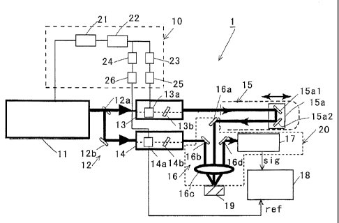
Fig. 1 is a block diagram illustrating the configuration of a
first embodiment of a delay-time-modulated pump probe measuring
device according to the present invention;
Fig. 2 is a chart illustrating the change with time of optical
intensity of the pump pulse light and the probe pulse light reaching
the surface of a sample with the measuring device in Fig. 1;
Fig. 3 is a chart illustrating the change of delay time of the
pump pulse light and the probe pulse light in Fig. 2 caused by pulse
8
CA 02670948 2009-05-28
English translation of PCT application
PCT/JP2007/072988
pickers;
Fig. 4 is a chart illustrating a relaxation process of measured
signals of a sample after being excited by the pump pulse light with
the measuring device in Fig. 1;
Fig. 5 is a block diagram illustrating the configuration of a
second embodiment of a delay-time-modulated pump probe
measuring device according to the present invention;
Fig. 6 is a block diagram illustrating the configuration of a
third embodiment of a delay-time-modulated pump probe measuring
device according to the present invention;
Fig. 7 is a block diagram illustrating the configuration of an
embodiment of a delay-time-modulated scanning probe microscope
apparatus having a time resolution of the order of femtosecond
according to the present invention;
Fig. 8 is a chart illustrating a noise spectrum of tunneling
current signals measured by a current-voltage conversion
preamplifier of a scanning tunneling microscope of a scanning probe
microscope apparatus in the embodiment as shown in Fig. 7; and
Fig. 9 is a chart illustrating a time-resolved tunneling
current of a low-temperature-grown GaNxAsi_x thin film measured
under a scanning probe microscope apparatus in the Example.
Description of the reference numerals
[00261
1, 30, 40: Pump probe measuring device
10, 10A, 10B: Delay time modulation unit
11, 31, 32: Laser source
12: Branch optical system
12a: Half mirror
12b: Reflecting mirror
13: First pulse picker
13a, 14a: Electro-optic element
13b, 14b: Light polarizer
14: Second pulse picker
15: Delay time adjusting unit
9
CA 02670948 2009-05-28
English translation of PCT application
PCT/JP2007/072988
15a: Movable mirror
16: Irradiation optical system
16a, 16b, 16d: Reflecting mirror
16c: Objective lens
17: Photosensor
18: Lock-in amplifier
19, 53: Sample
20: Measuring unit
21: Photosensor
22: Counting means
23, 24: Delaying means
25, 26: Driving means
33: Synchronous oscillation control unit
41: Cavity dumper
50: Scanning probe microscope apparatus
51: Irradiation optical system
51a: Half mirror
51b, 51c: Reflecting mirror
51d: Objective lens
52: Scanning tunneling microscope
52a: Probe
52b: Preamplifier
P1: Pump pulse light
P2: Probe pulse light
Best Modes for Carrying Out the Claimed Invention
[0027] Hereinafter, the present invention will be described in detail
with reference to certain embodiments thereof illustrated in the
drawings. In Figures, the same marks and symbols are used for
identical or corresponding members.
First, a delay-time-modulated pump probe measuring device
relating to a first embodiment of the present invention will be
described. Fig. 1 shows the configuration of a first embodiment of a
delay-time-modulated pump probe measuring device according to
the present invention. In Fig. 1, a delay-time-modulated pump probe
CA 02670948 2009-05-28
English translation of PCT application
PCT/JP2007/072988
measuring device 1 includes: an ultrashort optical pulse laser
generator including a laser source 11 for generating a first
ultrashort optical pulse train, which becomes pump light, and a
second ultrashort optical pulse train, which becomes probe light; a
branch optical system 12; two pulse pickers, namely a first pulse
picker 13 and a second pulse picker 14; a delay time modulation
unit 10 for periodically changing the position at which optical pulses
are transmitted by the pulse pickers 13 and 14; a delay time
adjusting unit 15; and an irradiation optical system 16, in addition
to a measuring unit 20 for detecting probe signal from a sample 19
to be measured, and a lock-in detection unit 18 to be connected to
the measuring unit 20.
[0028] The laser source 11 is a femtosecond pulse laser source, for
example. Specifically, a titanium sapphire laser oscillator capable of
generating laser pulses having wavelength of 800 nm, time width of
approximately 25 fs at the repetition frequency of approximately
100 MHz, and average luminance of approximately 1 W, can be used.
[0029] The branch optical system 12 includes a half mirror 12a
placed diagonally on the outgoing optical path of the laser pulses
coming from the laser source 11. The laser pulses from the laser
source 11 can be branched into a light transmitted through and a
light reflected by the half mirror 12a.
Here, the light transmitted through the half mirror 12a is
used as a pump light, whereas the light reflected by the half mirror
12a is used as a probe light. These may be reversed. Following
description assumes that the transmitted light is used as the pump
light, and the reflected light is used as the probe light.
In the Figure, the branch optical system 12 includes a
reflecting mirror 12b placed on the reflected light path, which
guides the reflected light into the second pulse picker 14.
[0030] The pulse pickers 13 and 14 include a first pulse picker 13, to
which the pump light from the branch optical system 12 is
introduced, and a second pulse picker 14, to which the probe light
from the branch optical system 12 is introduced. The pulse pickers
13 and 14 selectively transmit, at an arbitrary period, only one
11
CA 02670948 2009-05-28
English translation of PCT application
PCT/JP2007/072988
pulse among laser pulse trains coming in at the repetition frequency
as high as 100 MHz for example, and block the rest of the pulses. It
is preferable to set the intensity ratio of the transmitted light to the
blocked light as sufficiently high as 300:1 to 1,000:1.
[0031] The first pulse picker 13 and the second pulse picker 14 may
be of the same configuration, but various configurations can also be
selected on condition that each of them can extract a single light
pulse. In the case shown in the Figure, each of the pulse pickers 13
and 14 includes electro-optic elements 13a and 14a, which rotates a
polarization of the optical pulse by a voltage application, and light
polarizers 13b and 14b placed on the output side of the electro-optic
elements 13a and 14a. In the case of the Figure, a light polarizer
13b is placed on the output side, but the light polarizers can also be
placed on both input and output sides of the electro-optic element
13a. If acousto-optic devices are used instead of electro-optic
elements 13a and 14a to constitute the pulse pickers 13 and 14,
light polarizers 13b and 14b are unnecessary. The electro-optic
elements 13a and 14a are driven by the delay time modulation unit
10, which will be described later, to perform high-speed switching of
the order of nanosecond. In order to transmit pulses with
sufficiently high repetition rate, it is preferable that operating
frequency of up to 1 MHz can be selected. Consequently, a Pockels
cell can be used as each of the pulse pickers 13 and 14 and it may
block 99 pulses out of 100 and transmit the remaining one pulse.
This allows the effective repetition frequency of pulses
coming from the laser source 11 to decrease from 100 MHz to 1 MHz,
and the average laser intensity from 1 W to 10 mW. The timing of
transmission of optical pulses by the pulse pickers 13 and 14 will be
described later by referring to Fig. 2.
[0032] The delay time modulation unit 10 periodically changes the
selection position of the light pulses through the pulse pickers 13
and 14. For example, the delay time modulation unit 10 as shown in
Fig. 1 includes: a photosensor 21 for detecting optical pulses
generated from the ultrashort optical pulse laser generatorll; a
counting means 22 for counting pulse signals coming from the
12
CA 02670948 2009-05-28
English translation of PCT application
PCT/JP2007/072988
photosensor 21; a first delaying means 23 and a second delaying
means 24 to be connected to the counting means 22; and driving
means 25 and 26 for driving the pulse pickers 13 and 14. The first
and the second delaying means 23 and 24 may be placed on only one
side. If the pulse pickers 13 and 14 are Pockels cells, the driving
means 25 and 26 are high-voltage power supply devices.
[0033] A pin photodiode, an avalanche photodiode, or a
photomultiplier having a fast response capability, for example, can
be used as the photosensor 21, to ensure that it can respond to the
optical pulses from the ultrashort optical pulse laser generator. The
counting means 22 and the first and the second delaying means 23
and 24 can be composed of pulse circuits using transistors,
integrated circuits, microcomputers, etc., on condition that they can
periodically change the selection position of the light pulses which
transmit through the pulse pickers 13 and 14. If signals coming
from the fast photosensor 21 is used as a clock signal, a
microcomputer or a field programmable integrated circuit, i.e. a
complex programmable logic device (CPLD), can be used to
constitute the counting means 22 and the first and the second
delaying means 23 and 24 for driving an optical shutter such as an
electro-optic element to be used for the pulse pickers 13 and 14.
[0034] In the case shown in the Figure, the delay time adjusting
unit 15 is composed of an optical system of a known configuration
that adjusts the optical path length using a movable mirror 15a.
The movable mirror 15a can be a pair of reflecting mirrors placed at
the angle of 45 degrees against the incident light axis. A light
coming in along the incident light axis is reflected by one of the
reflecting mirrors 15a1 in the direction perpendicular to the
incident light axis, hits the other reflecting mirror 15a2, and is
reflected by the other reflecting mirror 15a2 in the direction parallel
to the incident direction.
[0035] The position of the movable mirror 15a can be adjusted in the
direction of the optical axis of the pump light pulses transmitted
through the first pulse picker (pump pulse light). If the movable
mirror 15a is transferred to right, the optical path length becomes
13
= CA 02670948 2009-05-28
English translation of PCT application
PCT/JP2007/072988
longer, whereas if it is transferred to left, the optical path length
becomes shorter.
Consequently, the delay time of the pump pulse light with
respect to the probe light pulses (probe pulse light) can be set as
any preferred time by moving the movable mirror 15a. For example,
if the movable range of the optical path length is approximately 30
cm, the delay time between the probe pulse light and the pump
pulse light can be set within the 0 to 1 ns range.
[0036] In the case shown in the Figure, the measuring unit 20
includes the irradiation optical system 16 and a photosensor 17 for
detecting probe signals from the sample 19. The irradiation optical
system 16 includes an objective lens 16c, which is placed near the
surface of the sample 19, a reflecting mirror 16a for guiding the
pump pulse light from the delay time adjusting unit 15 to the
surface of the sample 19, a reflecting mirror 16b for guiding the
probe pulse light from the second pulse picker 14 to the surface of
the sample 19, and a reflecting mirror 16d for guiding the probe
pulse light reflected on the surface of the sample 19 to the
photosensor 17. Thus, these configurations allow pump pulse light
and probe pulse light to focus on the surface of the sample 19. At
that time, the pump pulse light reaches the sample 19 first, and
immediately after that, the probe pulse light is reflected on the
surface of the sample 19.
[0037] Probe signals reflected on the surface of the sample 19 enter
the photosensor 17, reflected by the reflecting mirror 16d, and thus
the reflectance of the surface of the sample 19 can be measured at
the time when the precise delay time has elapsed after the pump
pulse light is irradiated. A Si pin photodiode can be used as the
photosensor 17, for example.
[0038] The lock-in detecting means can be composed of a lock-in
amplifier 18. The lock-in detecting means is used to perform
modulation measurement to ensure accuracy of measurement,
because the delay time-dependent component (see "sig" in Fig. 1) of
the reflected light intensity measured by the photosensor 17 is
extremely small compared with the fluctuation of the light intensity
14
= CA 02670948 2009-05-28
English translation of PCT application
PCT/JP2007/072988
of the laser source 11. The lock-in amplifier 18 performs a phase-
sensitive detection of the signals measured by the photosensor 17
using the modulation frequency of the delay time modulation
performed with the first and the second pulse pickers 13 and 14,
which will be described later by referring to Fig. 2, as a reference
signal (see "ref' in Fig. 1), thus enhancing measurement accuracy.
[0039] The features of the present invention include the pulse
pickers 13 and 14 and the delay time modulation unit 10, which
change periodically the selection positions of the light pulses which
transmit through the pulse pickers 13 and 14. The operation of the
delay time modulation unit 10 will be described below by referring
to Fig. 2.
Fig. 2 is a chart illustrating the optical intensity of the pump
pulse light P1 and probe pulse light P2 at the time when both reach
the surface of the sample 19. The abscissa axis of the chart
represents time, whereas the ordinate axis represents optical
intensity. Since the pump pulse light P1 and the probe pulse light
P2 are laser pulses from the laser source 11 having repetition
frequency of approximately 100 MHz, each laser intensity remains
at zero most of the time, and increases to a very high level for a
time period as short as 25 fs only.
[0040] Consequently, the pump pulse light P1 and the probe pulse
light P2 are illustrated as a comb-shaped chart as shown in Fig. 2.
If the repetition frequency of the laser pulses output from the
laser source 11 is 100 MHz, the time interval between pulses is 10
ns both for the pump pulse light P1 and the probe pulse light P2.
This time interval is expressed as the gap between dotted lines in
Fig. 2. Only one pulse out of 100 pulses is transmitted and the
remaining pulses are blocked by the operation of the pulse pickers
13 and 14. For convenience sake, one out of every 6 pulses is
transmitted, and remaining 5 are blocked in Fig. 2. The transmitted
light is expressed in a solid line, whereas the blocked light is
expressed in dotted line.
[0041] If delay time caused by the delay time adjusting unit 15 is
expressed as ¨At, the probe pulse light P2 lags behind the pump
CA 02670948 2009-05-28
English translation of PCT application
PCT/JP2007/072988
pulse light P1 by delay time At. At this time, the optical intensity
measured by the photosensor 17 is proportional to the reflectance R
(At) of the sample at the time precisely At after the excitation by the
pump pulse light Pl.
[0042] If the timing when the second pulse picker 14 transmits a
pulse is delayed by the period for 3 pulses as shown by P3 in Fig. 2,
the actual delay time is calculated to be At' --= At + 3 x 10 (ns), which
demonstrates that the delay time can be increased instantaneously
to a very large value. At this time, the optical intensity measured by
the photosensor 17 is proportional to the reflectance R (At') of the
sample. If the state as shown by P2 and P3 in Fig. 2 is repeated
periodically as shown in Fig. 3 by controlling the second pulse
picker 14, thus changing the passing position of the probe pulse
light, the signal measured by the photosensor 17 oscillates
periodically between R (At) and R (At'). The lock-in amplifier 18
performs the phase-sensitive detection of this signal, with the
modulation frequency used as a reference signal, which allows the
difference between R (At) and R (At') to be measured.
[0043] Since the delay time is modulated sinusoidally in the
conventional delay time modulation method, the signals obtained by
modulation measurement are expressed as average slope of R over
the entire modulation amplitude region (between At and At'). On the
contrary, the delay time modulation method according to the present
invention allows the delay time to be modulated into a precisely
rectangular waveform, and the obtained signal is exactly in
proportion to the difference between R (At) and R (At'), namely R
(At) ¨ R (At').
[0044] This gives a very advantageous point as described below.
Generally speaking, as shown in Fig. 4, the state of a sample
after being excited by the pump light approaches a certain value
after going through a relaxation time as short as several
picoseconds to several nanoseconds. In ultrafast measurement, the
amplitude and the duration of the relaxation time are targets of
measurement.
In this embodiment, if a value approximately half the pulse
16
CA 02670948 2009-05-28
English translation of PCT application
PCT/JP2007/072988
repetition period after pulse picking is adopted as delay time At' as
shown in Fig. 2, At' can take a very large value compared with the
relaxation time of the sample 19. Since At' is approximately 0.5 s,
for example, R (At') is considered to represent the state of the
sample 19 after the completion of relaxation, namely zero point of
the signal. At this time, the difference between R (At) and R (At')
measured in this embodiment, namely R (At) ¨ R (At'), is equal to R
(At) itself, and thus the absolute value of the delay time-dependent
component of reflectance can be obtained.
[0045] In addition, if the delay time between the pump pulse light
P1 and the probe pulse light P2 is changed by the delay time
adjusting unit 15 in Fig. 1, not only At but also At' changes.
However, as described previously, if a sufficiently large value is
selected as At', R (At') can be regarded as a constant, whereas R (At)
reflects fast relaxation process immediately after the excitation of
the sample. Consequently, the difference between R (At) and R (At')
represents the precise relaxation process of the sample 19 with
respect to the measured signal level after relaxation.
[0046] A delay-time-modulated pump probe measuring device related
to a second embodiment of the present invention will be described
below.
Fig. 5 illustrates the configuration of a delay-time-modulated
pump probe measuring device in a second embodiment of the present
invention. The delay-time-modulated pump probe measuring device
30 shown in Fig. 5 differs from the pump probe measuring device 1
as shown in Fig. 1 in that laser sources 31 and 32 are provided,
instead of the laser source 11, for the pump light and the probe light
respectively to eliminate the branch optical system 12 and the delay
time adjusting unit 15, that a first pulse picker 13 is driven by a
first delay time modulation unit 10A, and that a second pulse picker
13 is driven by a second delay time modulation unit 10B.
[0047] Each of the laser sources 31 and 32 has the same structure as
the laser source 11 in the pump probe measuring device 1 in Fig. 1,
and is controlled to oscillate at exactly the same periodicity by the
operation of a synchronous oscillation control unit 33. Since there is
17
CA 02670948 2009-05-28
English translation of PCT application
PCT/JP2007/072988
no need to branch the incident light to introduce them to each pulse
picker 13 and 14, the intensity of the pulse light applied to the
sample 19 is enhanced. In addition, the delay time of the two laser
pulses can be set freely by arbitrarily selecting the phase of the
optical pulse to be output. Two ultrashort optical pulse laser sources
31 and 32 can be made to have identical wavelength. If their
wavelengths differ from each other, the pump light and the probe
light can have different wavelengths. Furthermore, by setting the
oscillation phase of the pump light and the probe light as required
using the synchronous oscillation control unit 33 for two laser
devices, the delay time up to the repetition period can be set easily.
Consequently, since the delay time can be adjusted using the two
ultrashort optical pulse laser sources 31 and 32 and the two pulse
pickers 13 and 14, the delay time adjusting unit 15, which is
required when only one ultrashort optical pulse laser source is used,
can be omitted. For example, if the titanium sapphire oscillators
having repetition frequency of approximately 100 MHz are used as
the laser sources 31 and 32, the synchronous oscillation control unit
33 allows the pump pulse light P1 and the probe pulse light P2 to be
oscillated with the jitters of approximately 200 fs and with arbitrary
delay time of up to the pulse repetition period.
[00481 Since the delay time between the pump pulse light P1 and
the probe pulse light P2 can be set arbitrarily based on the
operation of the synchronous oscillation control unit 33, the delay
time adjusting unit 15 as shown in Fig. 1 can be omitted. The delay
time setting range, which was approximately 1 ns at maximum with
the pump probe measuring device 1 as shown in Fig. 1, can be
extended up to the pulse repetition period, and at the same time,
adverse effect such as slight deviation of optical axis due to
transition of mirrors over a long distance, etc. can be eliminated. By
adjusting the optical pulse transmission timing of the second pulse
picker 14, the delay time can be set arbitrarily within the effective
pulse repetition period after pulse picking, exceeding the base
repetition period of the laser sources 31 and 32. This will allow
measurement of relatively long relaxation time of several hundred
18
CA 02670948 2009-05-28
English translation of PCT application
PCT/JP2007/072988
nanoseconds to be conducted, even if laser sources 31 and 32 having
repetition frequency of 100 MHz is used.
[0049] The first delay time modulation unit 10A includes: a
photosensor 21 for detecting optical pulses generated by the first
laser source 31 of the ultrashort optical pulse laser generator, a
counting means 22 for counting pulse signals coming from the
photosensor 21, a first delaying means 23 to be connected to the
counting means 22, and a driving means 25 for driving the pulse
picker 13. Likewise, the second delay time modulation unit 10B has
a same configuration of the first delay time modulation unit 10A
and it includes: a photosensor 21 for detecting optical pulses
generated by the second laser source 32 of the ultrashort optical
pulse laser generator, a counting means 22, a second delaying
means 24, and a driving means 26 for driving the second pulse
picker 14. Since the photosensor 21, the counting means 22, the first
and the second delaying means 23 and 24, and the driving means 25
and 26 for the pulse pickers 13 and 14 can be structured in the same
way as the delay time modulation unit 10 described by referring to
Fig. 1, the description of these components will be omitted here.
Installation of only one of the first and the second delaying means
23 and 24 is allowed.
According to the first and the second delay time modulation
units 10A and 10B, the selection positions of the pulses passed by
the pulse pickers 13 and 14 can be changed periodically, as in the
case of the delay time modulation unit 10 as shown in Fig. 1.
[0050] The measuring device 30 in this configuration operates in the
same way as the measuring device 1 as shown in Fig. 1. In this case,
since two laser sources 31 and 32 are used, the equipment cost
increases, and the accuracy of delay time setting tends to decrease
compared with the measuring device 1 as shown in Fig. 1 due to the
limitation imposed by the synchronous oscillation control unit 33.
However, since the delay time setting can be made only by the
synchronous oscillation control unit 33, the mechanism of
mechanically moving the movable mirror 15a of the delay time
adjusting unit 15 in Fig. 1 is not required. Consequently, the
19
CA 02670948 2009-05-28
English translation of PCT application
PCT/JP2007/072988
reliability of the measuring system and the stability of the focal
point on the sample 19 improve significantly, which is the major
advantage of this configuration.
[0051] A third embodiment of a delay-time-modulated pump probe
measuring device related to the present invention will be described
below.
Fig. 6 illustrates the configuration of a delay-time-modulated
pump probe measuring device in a third embodiment of the present
invention. The delay-time-modulated pump probe measuring device
40 as shown in Fig. 6 differs from the pump probe measuring device
1 as shown in Fig. 1 in that a laser source 11 attached with a cavity
dumper 41 is used instead of the laser source 11.
[0052] The laser source 11, 41 equipped with the cavity dumper has
a known configuration. For example, a laser oscillator, where an
acousto-optic modulator (AO modulator) is inserted into a cavity of a
titanium sapphire laser, may be used. The highly intense optical
pulse can be output at low repetition frequency by opening the
cavity only once in several tens to several hundreds times of round
trip movements in the cavity of the laser and by taking out an
extremely intense laser pulse stored within the cavity, while
maintaining the average intensity at approximately the same level
as that of a conventional titanium sapphire laser oscillator.
According to this configuration, a laser oscillator having the average
intensity of several hundreds mW and repetition frequency of
approximately 2 MHz can be achieved.
[0053] If Pockels cells having the maximum operating frequency of 1
MHz are used as the two pulse pickers 13 and 14 in the first and the
second embodiments as shown in Figs. 1 and 5, only one of 100
optical pulses generated from the laser oscillator can be
transmitted. Consequently, the laser intensity decreases down to =
1/100. Even if the intensity of the laser from the laser sources 11,
31, and 32 is 1 W, the average intensity after passing the pulse
pickers 13 and 14 decreases to approximately 10 mW.
On the contrary, in the embodiment as shown in Fig. 6, since
the laser source 11, 41 has a repetition frequency of 2 MHz, for
CA 02670948 2009-05-28
English translation of PCT application
PCT/JP2007/072988
example, the pulse pickers 13 and 14 transmit one pulse in every
two pulses output from the laser source 11, thus decreasing the
repetition frequency from 2 MHz to 1 MHz and periodically
changing the optical pulses to be transmitted. Thus, the delay time
can be modulated as a rectangular waveform in the same manner as
the embodiment as shown in Fig. 1.
[0054] The measuring device 40 in this configuration operates in the
same manner as the measuring device 1 as shown in Fig. 1, with the
decrease of average intensity at the pulse pickers 13 and 14
maintained at approximately 50%. Probe light signal intensity much
higher than that of the embodiment shown in FIG. 1 can thus be
obtained.
[0055] Each embodiment described above assumes the case in which
the reflectance of the sample was measured by the rectangular-wave
pump probe modulation method. In addition to these methods, an
arbitrary time-resolved pump probe measurement method can be
combined with the rectangular-wave delay time modulation method
using pulse pickers. Consequently, capitalizing on the feature of the
present invention that measurement can be made over a wide delay
time range without modifying the intensity of pump probe light, a
microscope apparatus capable of measuring ultrafast phenomena
that occur in submicroscopic space can be achieved in combination
with a scanning tunneling microscope.
[0056] A scanning probe microscope apparatus using a delay-time-
modulated pump probe measuring device as a fourth embodiment of
the present invention will be described below.
Fig. 7 is a block diagram illustrating the configuration of one
of the embodiments of a delay-time-modulated scanning probe
microscope apparatus having a time resolution of the order of
femtosecond according to the present invention. A scanning probe
microscope apparatus 50 in Fig. 7 includes two laser sources 31 and
32, a synchronous oscillation control unit 33, a delay time
modulation unit 10, a first pulse picker 13 and a second pulse picker
14, an irradiation optical system 51, a scanning tunneling
microscope 52, and a lock-in amplifier 18.
21
CA 02670948 2009-05-28
English translation of PCT application
PCT/JP2007/072988
[0057] As shown in Fig. 7, the scanning probe microscope apparatus
50 according to the fourth embodiment of the present invention
differs from the pump probe measuring device according to the
second embodiment of the present invention as shown in Fig. 5 in
that a measuring unit 20 is equipped with the irradiation optical
system 51 and the scanning tunneling microscope 52.
[0058] The irradiation optical system 51 includes a half mirror 51a,
two reflecting mirrors 51b and 51c, and an objective lens 51d. The
pump pulse light coming from the first pulse picker 13 is reflected
by the reflecting mirror 51b, transmitted through the half mirror
51a, further reflected by the reflecting mirror 51c, and focused on a
surface of a sample 53 in the scanning tunneling microscope 52 via
the objective lens 51d. The probe pulse light coming from the second
pulse picker 14 is reflected by the half mirror 51a, overlapped with
the pump pulse on the same optical axis, further reflected by the
reflecting mirror 51c, and focused on the surface of the sample 53 in
the scanning tunneling microscope 52 via the objective lens 51d.
[0059] The scanning tunneling microscope 52 is a well-known
configuration provided with a probe 52a immediately above the
surface of the sample 53 to allow a tunnel junction to be formed
between the apex of the probe 52a and the sample 53. The probe 52a
is scanned on the surface of the sample 53. By applying laser pulses
to the surface of the sample 53, probe signals generated by
modulating the tunneling current between the apex of the probe 52a
and the sample 53 are detected by a preamplifier 52b for current
detection, and the amplified signal is output to the lock-in amplifier
18.
[0060] According to the microscope 50 having the above
configuration, laser pulses coming from the laser sources 31 and 32
are applied to the sample 53 placed immediately beneath the probe
52a, via the pulse pickers 13 and 14, and then via the irradiation
optical system 51, as the pump pulse light and the probe pulse light
respectively. In this case, pairs of laser pulses having delay time set
by the synchronous oscillation control unit 33 and the pulse pickers
13 and 14 excite the surface of the sample 53. At that time, to
22
= CA 02670948 2009-05-28
English translation of PCT application
PCT/JP2007/072988
maintain the tunneling current be+ween the probe 52a and the
sample 53 at a constant level, the scanning tunneling microscope 52
adjusts the gap between the probe 52a and the sample 53 by the
feedback control having a low cutoff frequency.
[0061] When the pulse pickers 13 and 14 are driven by the driving
means 25 and 26 to modulate the delay time, in order to avoid
signals targeted for measurement being attenuated by the feedback
control circuit, the modulation frequency of the pump pulse light is
kept sufficiently higher than the cutoff frequency of the feedback
control of the scanning tunneling microscope 52. In this state, when
the output signals coming from the preamplifier 52b for current
detection of the scanning tunneling microscope 52 is detected by the
lock-in amplifier 18, which is a phase sensitive detection, with
respect to the modulation frequency of the second pulse picker 14,
the ultrafast physical phenomenon occurring in submicroscopic
space on the surface of the sample 53 placed immediately beneath
the probe 52a can be observed as the output signals.
Examples
[0062] Examples of the delay-time-modulated pump probe measuring
device according to the present invention will be described below.
The basic principle of the measurement procedure of the
delay-time-modulated pump probe measuring device according to
the present invention is the same as that of the widely used
conventional delay-time-modulated pump probe measuring device,
but innovative improvement has been made to the modulation
method. Even if such improvement is made, the system operates
normally based on the basic operation principle governing the
conventional systems.
[0063] Of the embodiments shown above, the configuration of the
scanning probe microscope apparatus 50 as shown in Fig. 7 will be
described in details below.
The ultrafast time-resolved scanning tunneling microscope 50
is composed by combining the rectangular-wave-based delay time
modulation system using pulse pickers, which is the core of the
23
CA 02670948 2009-05-28
English translation of PCT application
PCT/JP2007/072988
present invention, and the r.onventional scanning tunneling
microscope.
[0064] First, the typical configuration of a conventional device used
for the same purpose will be described. As in the case of the
measuring unit 20 as shown in Fig. 7, since the pump pulse light
and the probe pulse light of the conventional device are also applied
to the sample on the identical optical axis, the sample is excited
repeatedly by pulse pairs consisting of two optical pulses, namely
the pump and the probe pulses. It is the reason why this type of
microscope is called the pulse-pair-excited time-resolved scanning
tunneling microscope. A delay-time-modulated optical pulse-pair-
excited scanning tunneling microscope apparatus is known as a
typical conventional device that mechanically oscillates the position
of mirrors included in a delay time setting optical system to perform
delay time modulation. When the sample placed under the scanning
tunneling microscope is excited using pulse pairs that have been
delay-time-modulated by mirror oscillation, a subpicosecond or
several tens picosecond ultrafast phenomena occurring in a
submicroscopic region of the order of nanometer can be measured.
With the conventional device of this type, however, the delay time
modulation amplitude is small and the modulation frequency is low,
which tends to lower the signal-noise ratio. Consequently, there was
a drawback that a single measurement required as long as several
hours to several tens hours.
The microscope apparatus 50 according to the embodiment of
the present invention as shown in Fig. 7 also employs the
configuration of the optical pulse-pair-excited scanning tunneling
microscope as in the case of a conventional device. Since the delay
time modulation system is improved as described above, the signal
intensity can be increased by raised modulation amplitude, the
noise intensity can be decreased by raised modulation frequency, the
time resolution is not negatively affected by the modulation
amplitude, and the deviation of the focal point of the laser from the
position of the probe of the scanning tunneling microscope due to
long-distance mirror transfer can be avoided.
24
CA 02670948 2009-05-28
English translation of PCT application
PCT/JP2007/072988
[0065] As a laser source 31 in Fig. 7, CHAMELEON by COHERENT
INC., and as the laser source 32, MIRA also by COHERENT, are
used. These two laser sources 31 and 32 are capable of
independently generating approximately 150 fs laser pulses at 90
MHz repetition frequency and average output power of 0.3 to 1.5 W
for 750 nm to 950 nm arbitrary wavelengths, respectively. The laser
sources 31 and 32 are allowed to oscillate synchronously at the jitter
of approximately 500 fs by using synchro-lock controller by
COHERENT as a synchronous oscillation control unit 33.
Furthermore, since the timing with respect to the phase of
oscillation can be arbitrary selected under the condition that the
oscillation intervals are fully synchronized, the delay time can be
set arbitrary over the entire pulse repetition period without
externally setting a delay time adjusting unit 15 employing long-
distance movable mirror transfer mechanism.
[0066] Pockels cells (RTP-3-20 by Laysop Ltd.) 13a and 14a were
used as the first and the second pulse pickers 13 and 14,
respectively. The switching time of each pulse pickers 13 and 14 was
approximately 1 ns, and the maximum repetition frequency was 1.5
MHz. One pulse can be picked up out of approximately 100 pulses
from 90 MHz pulse lasers generated by the laser sources 31 and 32.
Pockels cell drivers 25 and 26 (High Repetition-Rate Pockels Cell
Driver by ME) 25 and 26 were used as drive sources for driving
these Pockels cells 13a and 14a. The combination of these Pockels
cell drivers 25 and 26 and the Pockels cells (RTP-3-20) 13a and 14a
ensures repetition frequency of 1 MHz, which is appropriate for the
embodiment of the present invention.
[0067] The laser beam intensity immediately before the entry to the
pulse pickers 13 and 14 was detected by the fast photo diode 21
having a frequency band width of approximately 1 GHz to determine
the driving timing of the pulse pickers 13 and 14.
Detected intensity was used as clock signals to operate the delay
time modulation unit 10 including the CPLD, which is a
programmable integrated circuit, thus generating signals for
controlling the Pockels cell drivers 25 and 26, the driving means of
CA 02670948 2009-05-28
English translation of PCT application
PCT/JP2007/072988
the Pockels cells 13a and 14a of the pulse pickers 13 and 14.
Specifically, by transmitting one pulse out of every 90 pulses, the
laser pulse repetition frequency after transmission is set to 1 MHz.
In addition, the driving timing of the second pulse picker 14 only is
modulated by a half cycle (0.5 ,$) at the modulation frequency of
approximately 1 to 2 kHz.
[0068] Here, the modulation frequency must be sufficiently lower
than the bandwidth (up to tens of kHz) of the current detection
preamplifier 52b of the scanning tunneling microscope 52 on the
latter stage, and sufficiently higher than the weak feedback
bandwidth (up to 10 Hz) applied to the distance between the probe
52a of the scanning tunneling microscope 52 and the sample 53.
Consequently, the modulation frequency of approximately 1 to 2 kHz
is appropriate. Generally, when the phase-sensitive detection is
performed on tunneling current signals of the scanning tunneling
microscope, it is advantageous to set high modulation frequency in
order to avoid the noise due to the mechanical vibration. Since the
modulation frequency selected here, 1 to 2 kHz, is 50 to 100 times
higher than 20 Hz of the conventional delay-time-modulated system
employing mechanical mirror transfer method, the noise level will
be minimized to 1/5 to 1/10. Furthermore, by increasing the
modulation amplitude, which used to be 0.5 to 1 Ps, up to
approximately 0.5 [Is, the signal level is expected to increase to 10
times as high or higher. With both combined, the signal noise ratio
is expected to become several tens to several hundreds times higher.
[0069] The pump pulse light and the probe pulse light that have
passed through the pulse pickers 13 and 14 are overlapped on the
same optical axis by the half mirror 51a and reflecting mirrors 51b,
51c of the irradiation optical system 51, and then introduced to the
scanning tunneling microscope 52 via the objective lens 51d. The
diameter of the focal point of the laser beam on the surface of the
sample 53 should remain as small, and the distance from the
objective lens 51d to the focal point on the surface of the sample as
long, as possible, by using a composite optical system consisting of
multiple lenses as the objective lens 51d. Specifically, the beam
26
CA 02670948 2009-05-28
English translation of PCT application
PCT/JP2007/072988
diameter is expanded to 3 to 5 cm using a concave lens first, and
then it is narrowed down using a convex lens. This is a simple
method producing good results.
This allows the focal point diameter to be as small as several
[tm even when the distance from the objective lens 51d to the sample
51 is increased to approximately 300 mm. This design is necessary
to obtain sufficient light intensity while avoiding physical
interference between the scanning tunneling microscope 52 and the
objective lens 51d, and to minimize the disturbance in measurement
due to thermal expansion and contraction of the probe 52a, when
the apparatus is used in combination with a microscope capable of
obtaining measurements in a vacuum environment, in particular.
[0070] As the scanning tunneling microscope 52, a type capable of
carrying out measurement in an ultrahigh vacuum environment is
used to observe the surface of semiconductors, for example.
Normally, the ultrahigh vacuum scanning tunneling microscope
employs a vibration-free structure by suspending a detector unit
with a soft spring within the vacuum to prevent imperceptible
vibration of the floor from being transmitted to the measuring
device.
However, in implementing the present invention, if the
positional relation between the laser optical system for generating
delay-time-modulated pulse pairs and the detecting unit of the
scanning tunneling microscope deviates significantly, the relative
position of the sample 53, or probe 52a, and the focus of the
objective lens 51d, namely the irradiation position of the excitation
light source also deviates, thus adversely affecting measurement. It
is therefore preferable that the laser optical system and the
scanning tunneling microscope be placed on a large single vibration-
isolating board to minimize vibration coming from floor surface and
maintain proper mechanical and positional relation between them.
[0071] Results of measurement performed using the scanning probe
microscope apparatus 50 in the above example will be described
below.
As the sample 53 targeted for measurement, a GaNxAsi-x
27
= CA 02670948 2009-05-28
English translation of PCT application
PCT/JP2007/072988
(composition x here is 0.36%) thin film grown on a GaAs wafer at
low temperature by the molecular beam epitaxy method (MBE) was
cleaved on a (110) face, and its cross-sectional area was used for
measurement. Since the growth temperature of this sample was low,
its defect density was high. This defect plays a major role in
recombination of photo-carrier, and consequently, the fast
photocarrier relaxation process of approximately several tens
picoseconds to several hundreds picoseconds is expected.
[0072] Fig. 8 is a chart illustrating a noise spectrum of tunneling
current signals measured by the current-voltage conversion
preamplifier 52b of the scanning tunneling microscope 52 of the
scanning probe microscope apparatus 50 in the embodiment as
shown in Fig. 7. In Fig. 8, the abscissa axis indicates frequency
(Hz), whereas the ordinate axis indicates noise spectrum (A/Hz1/2).
As is obvious from Fig. 8, the noise density around 1 kHz
modulation frequency in delay time modulation using pulse pickers
in the scanning probe microscope apparatus 50 in this example is
approximately 1/10 of the noise density around 20 Hz modulation
frequency, which is used for a conventional delay-time-modulated
scanning tunneling microscope 52 employing mechanical mirror
vibration. It was thus confirmed that the increased modulation
frequency would decrease the noise level significantly.
[0073] Fig. 9 is a chart illustrating a time-resolved tunneling
current of a low-temperature-grown GaNxAsi_x thin film sample
measured under a scanning probe microscope apparatus 50 in the
example. In Fig. 9, the output from the lock-in amplifier 18 is
illustrated as the function of At (ps) as shown in Fig. 2, and the
ordinate axis indicates time-resolved tunneling current (fA). In this
case, At' in Fig. 2 was assumed to be approximately 0.5 is.
As described previously, the output signal from the lock-in
amplifier 18 represents delay-time-dependent component I (At) of
the tunneling current value itself for sufficiently large At', reflecting
ultrafast response in a nm-scale submicroscopic region immediately
beneath the probe 52a of the scanning tunneling microscope 52
placed on the sample 53, mostly the relaxation process of the
28
CA 02670948 2009-05-28
English translation of PCT application
PCT/JP2007/072988
photocarrier. As is obvious from Fig. 9, the ultrafast relaxation
process that occurs in several tens or several hundreds picoseconds
can be detected as a change in femtoampere (fA) order tunneling
current. It was found that the signal noise ratio at this time was
approximately 100 times higher than that of conventional devices.
Industrial Applicability
[0074] The present invention significantly improves the delay time
modulation method of the conventional delay-time-modulated pump
probe measurement method, which has thus far been used widely.
From the perspective that the application of ultrafast phenomena
will become increasingly important in the future, the present
invention is of great significance and its scope of application is
extremely wide. In the pump light intensity modulation, for
example, sample temperature fluctuates significantly, thus
adversely affecting measurement results. However, by using the
method achieved by the present invention, the measurements can be
performed with the sample temperature kept almost constant.
[0075] A femtosecond time-resolved scanning probe microscope
according to the present invention is expected to ensure the signal
noise ratio approximately 100 times higher than that of
conventional microscopes. Since the measurement can be made
while a temperature of the sample is maintained at approximately
the same level, dramatic development is expected. For example, a
carrier lifetime and carrier transfer in a picosecond region within
semiconductor nano-devices can be measured, and means of
measurement thus far unavailable will be provided. Gaining deeper
understanding of new physical phenomena capitalizing on the
present invention would be of significant importance in the research
phase of devices providing new functions. The wide scope of
application of the present invention also includes on-site use for
evaluating fabricated devices.
The pump probe device of the present invention can also be
used as various types of measuring apparatus, attached to
measuring devices such as scanning electron microscope and
29
CA 02670948 2009-05-28
English translation of PCT application
PCT/JP2007/072988
transmission electron microscope.