Note: Descriptions are shown in the official language in which they were submitted.
CA 02671231 2009-05-29
DESCRIPTION
Schottky Barrier Diode
TECIMICAL FIELD
The present invention relates generally to Schottky barrier diodes and
particularly to Schottky barrier diodes having improved reverse withstand
voltage.
BACKGROUND ART
Gallium nitride (GaN) has excellent characteristics in comparison with silicon
(Si). For example, the former has a band gap approximately three times that of
the
latter, a high breakdown electric field intensity approximately 10 times that
of the latter,
and larger saturation electron velocity, and the like. GaN is expected to
simultaneously
establish both high withstand voltage and small loss, i.e., low on-resistance,
that
conventional Si power devices can hardly achieve. GaN is thus expected to be
applied
to power devices (power semiconductor devices).
Conventionally, there have been proposed Schottky barrier diodes (SBDs), pn
junction diodes, metal-insulator-semiconductor (PvBS) transistors arid other
semiconductor devices that employ a GaN substrate (see Japanese Patent Laying-
Open
No. 2006-100801 (Patent Document 1) for example). Conventionally, power
devices
have employed a material of GaN generally in the form of a GaN epitaxial layer
deposited on a substrate of sapphire, silicon carbide (SiC) or the like, i.e.,
different in
composition. In contrast, a GaN epitaxial layer deposited on a GaN substrate
has a
lower impurity concentration and a lower dislocation density than a GaN
epitaxial layer
deposited on a substrate different in composition. Accordingly it is disclosed
that
epitaxial growth of GaN on a GaN substrate can implement a high withstand
voltage and
low on-resistance power device (see Tatsuya TANABE et al, "Epitaxial Growth of
GaN
on GaN Substrate and Its Application to Power Device", SEI Technical Review,
No.
170, (Non Patent Document 1) for example).
-1-
CA 02671231 2009-05-29
Furthermore, a field plate (FP) structure is disclosed as a structure for
reducing
or preventing an electric field that is concentrated at an end portion of an
electrode of a
power device to achieve high withstand voltage (see Yoshiharu TAKADA et al,
"AIGaN/GaN HEMT power device", Toshiba Review, Vol. 59, No. 7 (Non Patent
Document 2) for example).
Patent Document 1: Japanese Patent Laying-Open No. 2006-100801
Non Patent Document 1: Tatsuya TANABE et al, "Epitaxial Growth of
GaN on GaN Substrate and Its Application to Power Device", SEI Technical
Review,
No. 170, January 2007, pp. 34-39
Non Patent Document 2: Yoshiharu TAKADA et al, "AlGaN/GaN HEMT
power device", Toshiba Review, Vol. 59, No. 7, July 2004, pp. 35-38
DISCLOSURE OF THE INVENTION
PROBLEMS TO BE SOLVED BY THE INVENTION
The present inventors have furthered studying for a Schottky barrier diode
(SBD) employing a GaN substrate to achieve high withstand voltage. As a
result, the
present inventors have clarified for the first time that applying a field
plate (FP) structure
to an SBD fabricated with a GaN epitaxial layer deposited on a substrate
diPierer,t i1-1
composition such as a Si substrate or a sapphire substrate for example does
not achieve
a small leak current. In other words, if an SBD is fabricated with a GaN
epitaxial layer
deposited on a substrate different in composition, as a GaN material for a
power device
has conventionally, generally been done so, an FP structure applied to that
SBD does
not alleviate an electric field that is concentrated at an end of a Schottky
electrode, and a
sufficiently effectively decreased reverse leak current and sufficiently
effectively
increased reverse withstand voltage thus cannot be achieved.
Therefore, the present invention mainly contemplates a Schottky barrier diode
that allows a field plate structure to alleviate a concentrated electric field
and thus
effectively achieve increased reverse withstand voltage.
MEANS FOR SOLVING THE PROBLEMS
-2-
CA 02671231 2009-05-29
The present inventors have studied why an FP structure applied to an SBD
fabricated with a GaN epitaxial layer deposited on a substrate different in
composition
does not sufficiently effectively alleviate an electric field. As a result,
the present
inventors have inferred that as a substrate different in composition such as a
Si substrate,
a sapphire substrate, and GaN have different crystalline structures, a GaN
epitaxial layer
deposited has a high dislocation density exceeding 1 x 108 cm z, and
accordingly, the
present inventors have provided the present invention configured as follows:
The present invention in one aspect provides a Schottky barrier diode
comprising: a gallium nitride substrate having a major surface; an epitaxial
layer
deposited on the major surface; an insulation layer deposited on a surface of
the epitaxial
layer and having an opening; a Schottky electrode deposited in the opening in
contact
with the epitaxial layer; and a field plate electrode connected to the
Schottky electrode
and also overlapping the insulation layer, wherein the gallium nitride
substrate has a
dislocation density of at most 1 x 108 cm"2.
Employing a gallium nitride substrate having a low dislocation density of at
most
I x 108 cm'2 reduces dislocation in the epitaxial layer. Accordingly in a
Schottky
barrier diode having a field plate structure, the field plate structure
alleviates an electric
field under the condition that a reverse leak current is reduced. As a result,
the reverse
leak current is further reduced and increased reverse withstand voltage can be
achieved.
It is preferable that the gallium nitride substrate has lower dislocation
density. For
example, it is more preferable that the gallium nitride substrate has a
dislocation density
of at most 1 x 106 cm"z. Note that in the state of the art the gallium nitride
substrate's
dislocation density has a lower limit value of approximately 1 x 103 cm"2.
The present invention in another aspect provides a Schottky barrier diode
comprising: a gallium nitride layer having a front surface; an insulation
layer deposited
on the gallium nitride layer at the front surface and having an opening; a
Schottky
electrode deposited in the opening in contact with the gallium nitride layer;
and a field
plate electrode connected to the Schottky electrode and also overlapping the
insulation
-3-
CA 02671231 2009-05-29
layer, wherein the gallium nitride layer has a region in contact with the
Schottky
electrode, the region having a dislocation density of at most 1 x 108 cm 2.
The gallium nitride layer is in contact with the Schottky electrode at a
region
having a low dislocation density of at most 1 x 108 cm'2. Accordingly in a
Schottky
barrier diode having a field plate structure, the field plate structure
alleviates an electric
field under the condition that a reverse leak current is reduced. As a result,
the reverse
leak current is, further reduced and increased reverse withstand voltage can
be achieved.
It is preferable that the region of the gallium nitride layer that is in
contact with the
Schottky electrode has lower dislocation density.
A field plate structure, as referred to herein, indicates a structure
configured by
an insulation layer and a field plate electrode deposited on the insulation
layer. The
field plate electrode is electrically connected to the Schottky electrode, and
the Schottky
electrode and the field plate electrode are equal in potential. The field
plate structure
alleviates an electric field concentrated at an end portion of the Schottky
electrode in
operation as a cause of destroying a device, and thus allows the Schottky
barrier diode
to achieve high withstand voltage and high output. The insulation layer can be
formed
of material such as SiNX for example.
In the above one aspect preferably the Schottky barrier diode further
comprises
an ohmic electrode deposited on a rear surface opposite to the major surface
and has a
vertical structure allowing a current to flow from one of the Schottky
electrode and the
ohmic electrode to the other of the Schottky electrode and the ohmic
electrode.
In the above other aspect preferably the Schottky barrier diode further
comprises
an ohmic electrode deposited on the gallium nitride layer at a rear surface
opposite to
the front surface and has a vertical structure allowing a current to flow from
one of the
Schottky electrode and the ohmic electrode to the other of the Schottky
electrode and
the ohmic electrode.
In general, for a power device, a vertical structure can flow a larger current
than
a lateral structure, and the vertical structure is a more suitable structure
for the power
-4-
CA 02671231 2009-05-29
device. Sapphire is insulative, and a power device employing a sapphire
substrate
cannot be provided in a vertical structure. In accordance with the present
invention, a
gallium nitride substrate and a gallium nitride layer are electrically
conductive, and a
vertical structure having an ohmic electrode deposited at a rear surface can
be
implemented.
Furthermore in the above one aspect preferably the Schottky barrier diode has
the insulation layer having an end face facing the opening and inclined
relative to a front
surface of the epitaxial layer at an angle of at least 0.1 and at most 60 ,
and has the
field plate electrode overlapping the insulation layer in contact with the end
face of the
insulation layer.
In the above other aspect preferably the Schottky barrier diode has the
insulation
layer having an end face facing the opening and inclined relative to the front
surface of
the gallium nitride layer at an angle of at least 0.1 and at most 60 , and
has the field
plate electrode overlapping the insulation layer in contact with the end face
of the
insulation layer.
The insulation layer has an end face inclined relative to a surface of the
epitaxial
layer or that of the gallium nitride layer, and the field plate structure can
more effectively
alleviate an electric field. The Schottky barrier diode can achieve further
improved
reverse withstand voltage.
A smaller inclination angle allows the field plate structure to more
effectively
alleviate an electric field and hence improve withstand voltage. If the
inclination has an
angle of less than 0.1 , however, the angle is poor in reproducibility, which
may result in
a problem in fabrication. Furthermore, the field plate electrode that does not
have a
current flowing therethrough is large relative to the Schottky electrode. This
requires a
material excessively, which is disadvantageous in fabrication. In contract,
the
inclination having an angle exceeding 60 reduces the effect of alleviating
the electric
field. It is more preferable that the inclination angle is at least 1 and at
most 30 .
The insulation layer can have the end face inclined by wet etching, dry
etching or the like.
-5-
CA 02671231 2009-05-29
Furthermore in the above one and other aspects preferably the Schottky barrier
diode has the Schottky electrode formed of a material including at least one
type of
substance selected from the group consisting of gold (Au), platinum (Pt),
nickel (Ni),
palladium (Pd), cobalt (Co), copper (Cu), silver (Ag), tungsten (W) and
titanium (Ti).
The Schottky electrode that is formed of these materials such as gold can
implement a
low leak current Schottky electrode, and the field plate structure alleviates
an electric
field. As a result, a reverse leak current is reduced and reverse withstand
voltage is
increased.
Furthermore in the above one and other aspects preferably the Schottky barrier
diode has the insulation layer having a thickness of at least 10 nm and at
most 5 m. If
the insulation layer has a thickness of less than 10 nm, the insulation layer
has low
withstand voltage. Accordingly, the insulation layer is first destroyed and
the field
plate structure's effect cannot be obtained. If the insulation layer has a
thickness
exceeding 5 m, the alleviation per se of an electric field by the field plate
structure
cannot be obtained. The insulation layer more preferably has a thickness of at
least 0.2
m and at most 2 m for example for a design with a withstand voltage of 1 W.
Furthermore in the above one and other aspects preferably the Schottky barrier
diode has the field plate electrode overlapping the insulation layer along a
length of at
least 1 m and at most 1 mm. If the length is less than 1 m, it is difficult
to control,
and the field plate structure's effect cannot be obtained reliably. If the
length exceeds 1
mm, the alleviation per se of an electric field by the field plate structure
cannot be
obtained. The length is more preferably at least 5 m and at most 40 m, as a
depletion layer has a width extending to at least 2 m and at most 20 m for
example
for a design with a withstand voltage of 1 W.
EFFECTS OF THE INVENTION
The present Schottky barrier diode allows a field plate structure to alleviate
a
concentrated electric field and as a result can reduce a reverse leak current
and thus
achieve increased reverse withstand voltage effectively.
-6-
CA 02671231 2009-05-29
BRIEF DESCRIPTION OF THE DRAWINGS
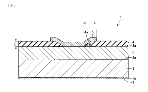
Fig. 1 is a cross section of a Schottky barrier diode in a first embodiment of
the
present invention.
Fig. 2 is a perspective view of the Fig. 1 Schottky barrier diode.
Fig. 3 shows in a flowchart each step of a method of fabricating the Schottky
barrier diode of the first embodiment of the present invention.
Fig. 4 is a cross section of a Schottky barrier diode in a second embodiment
of
the present invention.
Fig. 5 shows in a flowchart each step of a method of fabricating the Schottky
barrier diode of the second embodiment of the present invention.
Fig. 6 is a cross section of an SBD that does not have an FP structure.
Fig. 7 is a cross section of an SBD that employs a sapphire substrate.
DESCRIPTION OF THE REFERENCE SIGNS
1, 11: Schottky barrier diode, 2: GaN freestanding substrate, 2a: front
surface,
2b: rear surface, 3: GaN epitaxial layer, 3a: front surface, 3c: region, 4:
insulation layer,
4a: end face, 5, 6, 25, 36: electrode, 12: GaN underlying layer, 13: support
substrate,
32: sapphire substrate, 34: insulation layer.
BEST MODES FOR CARRYING OUT THE INVENTION
Hereinafter reference will be made to the drawings to describe the present
invention in embodiments. In the following description, identical or
corresponding
components are denoted by identical reference characters and will not be
described
repeatedly.
First Embodiment
Fig. 1 is a cross section of a Schottky barrier diode in a first embodiment of
the
present invention. Fig. 2 is a perspective view of the Fig. 1 Schottky barrier
diode.
As shown in Fig. 1 and Fig. 2, a Schottky barrier diode (SBD) 1 includes a GaN
freestanding substrate 2 serving as a gallium nitride substrate, and a GaN
epitaxial layer
3 serving as an epitaxial layer. GaN epitaxial layer 3 is deposited on GaN
freestanding
-7-
CA 02671231 2009-05-29
substrate 2 at a front surface 2a serving as a major surface. SBD 1 also
includes an
insulation layer 4. Insulation layer 4 is deposited on GaN epitaxial layer 3
at a front
surface 3 a.
SBD 1 further includes an electrode 5 in contact with front surface 3a of GaN
epitaxial layer 3 and also overlapping insulation layer 4, and an electrode 6
adjacent to a
rear surface 2b of GaN freestanding substrate 2. Insulation layer 4 has an
opening and
electrode 5 is provided in the opening of insulation layer 4. Electrode 5 is
formed for
example to be round in a plane.
Electrode 5 includes a Schottky electrode and a field plate (FP) electrode.
The
Schottky electrode is a portion internal to the opening of insulation layer 4
and in
contact with front surface 3 a of GaN epitaxial layer 3. The FP electrode is a
portion
overlapping insulation layer 4. The field plate electrode and insulation layer
4 form a
field plate structure. Furthermore, the Schottky electrode cooperates with GaN
epitaxial layer 3 to provide Schottky junction. Electrode 6 is an ohmic
electrode
cooperating with GaN freestanding substrate 2 to provide ohmic junction.
GaN freestanding substrate 2 has a dislocation density of at most 1 x 108 cm
Z.
Furthermore, electrode 5 is formed of a material (i.e., the Schottky electrode
is formed
of a material) including at least one type of substance selected from the
group consisting
of gold, platinum, nickel, palladium, cobalt, copper, silver, tungsten and
titanium. GaN
freestanding substrate 2 having the low dislocation density of at most 1 x 10⁸
cm"2
allows GaN epitaxial layer 3 to also have a dislocation density equivalent to
that of GaN
freestanding substrate 2, i.e., at most 1 x 10 8 cm z. SBD 1 having the FP
structure thus
has the FP structure significantly alleviating an electric field under the
condition that a
reverse leak current is reduced and the condition that a Schottky electrode
formed of an
electrode such as gold, which can implement a small leak current, is employed.
As a
result, the reverse leak current can further be reduced and increased reverse
withstand
voltage can be achieved. Note that a dislocation density can be measured for
example
by counting the number of pits formed by etching in melted KOH, and dividing
the
-8-
CA 02671231 2009-05-29
counted number by a unit area.
Furthermore, SBD 1 has a vertical structure allowing a current flowing from
one
of the Schottky electrode and the ohmic electrode to the other thererof. In
general, for
a power device, a vertical structure can flow a larger current than a lateral
structure, and
the vertical structure is a more suitable structure for the power device. In
SBD 1, GaN
freestanding substrate 2 and GaN epitaxial layer 3 are electrically
conductive, and a
vertical structure having the ohmic electrode provided at the rear surface can
be
provided.
Insulation layer 4 can be formed of silicon nitride film (SiNx). Furthermore,
insulation layer 4 can contain hydrogen having a concentration of less than
3.8 x 10²²
cm"3, more preferably less than 2.0 x 1022 cm"3. Thus, SiNX having a low
concentration
of hydrogen in the film can be applied as an insulation film forming the FP
structure.
The insulation layer with a low concentration of hydrogen is more effective
than that
with a high concentration of hydrogen in that the FP structure alleviates an
electric field
that is concentrated at an end of the Schottky electrode to achieve
effectively increased
reverse withstand voltage. In other words, SBD 1 can significantly effectively
alleviate
an electric field and achieve increased reverse withstand voltage.
Fig. 1 shows insulation layer 4 having a thickness represented by t.
Desirably,
insulation layer 4 has thickness t of at least 10 nm and at most 5 m. If
insulation layer
4 has thickness, t of less than 10 nm, insulation layer 4 has low withstand
voltage.
Accordingly, insulation layer 4 is first destroyed and the FP structure's
effect cannot be
obtained. If insulation layer 4 has a thickness exceeding 5 m, the
alleviation per se of
an electric field by the FP structure cannot be obtained.
Furthermore, Fig. 1 indicates a dimension L, which indicates the field plate's
length. The field plate's length indicates that length of the field plate
electrode which
overlaps insulation layer 4. In the present embodiment the FP length is a
length along
which the FP electrode overlaps insulation layer 4 in a cross section of SBD
1, as shown
in Fig. 1, that traverses the center of electrode 5 round in geometry in a
plane. In other
-9-
CA 02671231 2009-05-29
words, when insulation layer 4 has an opening round in geometry in a plane and
electrode 5 has a portion, or the Schottky electrode, round in geometry in the
plane, the
FP length is a length along which the FP electrode overlaps insulation layer 4
in the
Schottky electrode's radial direction.
In other words, the field plate's length refers to a length along which the
field
plate electrode overlaps the insulation layer in a direction of a straight
line connecting a
barycenter for the geometry of the Schottky electrode in the plane and one
point present
on the geometry's perimeter. Desirably, such an FP length is at least 1 m and
at most
1 mm. If the FP length is less than 1 m, it is difficult to control, and the
FP structure's
effect cannot be obtained reliably. If the FP length exceeds 1 mm, the
alleviation per se
of an electric field by the FP structure cannot be obtained.
Furthermore, as shown in Fig. 1, insulation layer 4 has an end face 4a facing
the
opening serving as a portion having electrode 5 in contact with GaN epitaxial
layer 3.
End face 4a inclines to form an angle 0 relative to front surface 3 a of GaN
epitaxial layer
3. The portion of electrode 5 that overlaps insulation layer 4, i.e., the FP
electrode, is
overlapped on insulation layer 4 in contact with end face 4a.
End face 4a inclined relative to front surface 3a allows the FP structure to
more
effectively alleviate an electric field and hence SBD 1 to have further
improved reverse
withstand voltage. Insulation layer 4 can have end face 4a inclined, as
described above,
by wet etching, dry etching or the like. End face 4a is formed to have angle 0
of at
least 0.1 and at most 60 . If the inclination has an angle of less than 0.1
, the angle is
poor in reproducibility, and furthermore, an excessive material is required,
which may
result in a problem in fabrication. In contrast, the inclination having an
angle exceeding
60 reduces the effect of alleviating an electric field.
Hereinafter, a method of fabricating SBD 1 will be described. Fig. 3 shows in
a
flowchart each step of a method of fabricating the Schottky barrier diode of
the first
embodiment of the present invention. With reference to Fig. 1 to Fig. 3, the
method of
fabricating a Schottky barrier diode of the present invention will be
described.
-10-
CA 02671231 2009-05-29
Initially, with reference to Fig. 3, a step (S 10) is performed to provide a
semiconductor layer. More specifically, there is prepared an n conduction
type, (0001)
plane GaN freestanding substrate 2 deposited by hydride vapor phase epitaxy
(HVPE).
GaN freestanding substrate 2 has a carrier density for example of 3 x 1018 cm
3, a
thickness for example of 400 m, and an average dislocation density for
example of 1 x
106 cm 2. Subsequently in step (S20) an epitaxial layer is deposited. More
specifically,
on GaN freestanding substrate 2, an n conduction type epitaxial layer is grown
by
organo-metallic vapor phase epitaxy (OMVPE) to have a carrier density for
example of
5 x 1015 cm"3 and a thickness for example of 7 m to deposit a GaN epitaxial
layer 3.
GaN epitaxial layer 3 has an average dislocation density similar for example
to that of
GaN freestanding substrate 2, i.e., 1 x 106 cm"z.
Subsequently in step (S30) an insulation layer is deposited. More
specifically,
on GaN epitaxial layer 3, an insulation layer 4 is deposited by depositing
SiNx by plasma
chemical vapor deposition (plasma CVD). Insulation layer 4 has thickness t of
approximately 1 m. In doing so, a source gas of ammonia (NH3) is used and
SiNX is
deposited from monosilane (SiH4), NH3, and hydrogen (H2). Depositing SiNX from
SiH4 and NZ without using NH3 is preferable, as such can reduce the
concentration of
the hydrogen in insulation layer 4.
Subsequently in step (S40) an ohmic electrode is deposited. More specifically,
GaN freestanding substrate 2 has rear surface 2b cleaned organically and
cleaned with
hydrochloric acid and thereafter Ti/Al/Ti/Au (20 nm/100 nm/20 nm/200 nm) is
deposited by electron beam deposition (EB deposition) on the entirety of rear
surface 2b.
Subsequently in an ambient of nitrogen the intermediate product is heated for
approximately 2 minutes to 600 C and alloyed to provide electrode 6 serving as
the
ohmic electrode.
Subsequently in step (S50) the insulation layer etched. More specifically,
photolithography is employed to provide a pattern on insulation layer 4.
Subsequently,
buffered hydrogen fluoride (BHF) is used to wet etch insulation layer 4.
Subsequently,
-11-
CA 02671231 2009-05-29
the intermediate product is cleaned organically and ashed in an ambient of
oxygen and
nitrogen to remove a resist. Insulation layer 4 is thus etched and thus
provided with an
opening. At this point of time, the opening exposes GaN epitaxial layer 3. The
opening can be formed for example to have a side surface having the geometry
of a
circular conical surface of a truncated cone having a maximal value of 200 m
in
diameter.
Subsequently in step (S60) a Schottky electrode and an FP electrode are
deposited. More specifically, photolithography is employed to pattern the
intermediate
product. Subsequently, it is cleaned with hydrochloric acid to treat a surface
of GaN
epitaxial layer 3 at room temperature for 3 minutes, and thereafter, as a
material for an
electrode, Au (400 nm) is deposited by resistance heating deposition.
Subsequently
when a resist is removed the material of the electrode deposited on the resist
is
simultaneously removed (lifted off) and electrode 5 is thus deposited.
Electrode 5 can
be formed to have a geometry larger in diameter than the opening formed in
insulation
layer 4. For example, it can be formed in a circle having a diameter of 220 m
in a
plane.
Thus, a Schottky electrode that is a portion provided in the opening of
insulation
layer 4 in contact with front surface 3a of GaN epitaxial layer 3, and an FP
electrode
that is a portion connected to the Schottky electrode and also overlapping
insulation
layer 4, are provided. In other words, electrode 5 is larger in diameter than
the
opening of insulation layer 4 and thus has a portion overlapping insulation
layer 4 to
provide the FP electrode.
By the above described fabrication method the Fig. 1 and Fig. 2 SBD 1 can be
fabricated. SBD 1 fabricated in this method has a semiconductor layer provided
in step
(S 10) employing GaN freestanding substrate 2 having a low dislocation density
of at
most 1 x 108 cm 2 to allow GaN epitaxial layer 3 to have a low dislocation
density.
Furthermore, it has a Schottky electrode provided in step (S60) using gold as
a material
therefor (i.e., a material for electrode 5). As a result a reverse leak
current is reduced
-12-
CA 02671231 2009-05-29
and increased reverse withstand voltage can be achieved.
In the above described SBD fabrication method step (S60) is performed to
deposit a Schottky electrode and an FP electrode simultaneously. Alternatively
there
may be provided a step of depositing the Schottky electrode and, subsequently,
a step of
depositing the FP electrode. More specifically, with reference to Fig. 1 and
Fig. 2, the
Schottky electrode may be deposited in the opening of insulation layer 4 in
contact with
GaN epitaxial layer 3 and the FP electrode may then be deposited to connect to
the
Schottky electrode and also overlap insulation layer 4. In that case, the FP
electrode
may be formed of the same material(s) as the Schottky electrode.
Alternatively, the FP
electrode may be formed of a material different from that of the Schottky
electrode,
such as a material satisfactorily adhesive to insulation layer 4.
Second Embodiment
Fig. 4 is a cross section of a Schottky barrier diode in a second embodiment
of
the present invention. As shown in Fig. 4, the present embodiment provides a
Schottky
barrier diode (SBD) 11 basically similar in configuration to Schottky barrier
diode 1 of
the first embodiment, except that the former excludes GaN freestanding
substrate 2.
More specifically, Schottky barrier diode 11 includes a support substrate 13,
a
GaN underlying layer 12, GaN epitaxial layer 3, insulation layer 4, a Schottky
electrode,
and a field plate electrode. A region 3c in contact with the Schottky
electrode in GaN
epitaxial layer 3 has a dislocation density of at most 1 x 108 cm'2.
Support substrate 13 is an electrically conductive substrate. Support
substrate
13 underlies GaN underlying layer 12. GaN underlying layer 12 underlies GaN
epitaxial layer 3. Note that support substrate 13 and GaN underlying layer 12
together
make ohmic contact. If support substrate 13 is formed of metal, electrode 6
may be
dispensed with. The remainder in configuration is similar to the first
embodiment.
Accordingly, it will not be described repeatedly.
SBD 11 is fabricated in a method, as will be described hereinafter. Fig. 5
shows in a flowchart each step of a method of fabricating the Schottky barrier
diode of
- 13 -
CA 02671231 2009-05-29
the second embodiment of the present invention. The method of fabricating SBD
11 in
the present embodiment is basically similar in configuration to the method of
fabricating
SBD 1 as described in the first embodiment, except that the former further
includes the
step of removing a GaN freestanding substrate.
Mare specifically, similarly as done in the first embodiment, a semiconductor
layer deposition step (S 10) is performed to prepare GaN freestanding
substrate 2.
Then an ion injection step (S70) is performed to inject an impurity in the
form of ions to
GaN freestanding substrate 2 at front surface 2a or rear surface 2b. This
provides GaN
freestanding substrate 2 in a vicinity of front surface 2a or rear surface 2b
with a layer
containing the impurity in a large amount. Subsequently, a support substrate
deposition step (S80) is performed to bond the surface having the ions
injected thereto
and support substrate 13 together. Subsequently, a heat treatment step (S90)
is
performed to subject GaN freestanding substrate 2 and support substrate 13
that are
bonded together to a heat treatment. This splits GaN freestanding substrate 2
such that
the region of GaN freestanding substrate 2 that contains the impurity in the
large amount
serves as a boundary. As a result, support substrate 13, and GaN underlying
layer 12
overlying support substrate 13 and smaller in thickness than GaN freestanding
substrate
2 can form a substrate. The SBD requires only a portion of expensive GaN
freestanding substrate 2 and the remainder of the substrate can be reused. The
SBD
can thus be fabricated at reduced cost.
Subsequently, an epitaxial layer deposition step (S20) is performed to deposit
GaN epitaxial layer 3 on GaN underlying layer 12. GaN epitaxial layer 3 is in
contact
with a Schottky electrode at a region having a dislocation density of at most
1 x 108 cm"
z
Note that while in the present embodiment, GaN freestanding substrate 2 is
used
to provide GaN underlying layer 12, and furthermore, GaN underlying layer 12
is used
to provide GaN epitaxial layer 3, the present invention is not limited
thereto.
Example
-14-
CA 02671231 2009-05-29
Hereinafter an example of the present invention will be described. As the
present invention's SBD, SBD I described above is fabricated and subjected to
an
experiment measuring its reverse withstand voltage. SBD 1 is fabricated
specifically in
a method and has a size and other characteristics, as has been described with
reference
to Fig. 1 to Fig. 3, and the FP length is set at 10 m and insulation film 4
has end face
4a inclined relative to front surface 3a of GaN epitaxial layer 3 at angle 0
set at 11 .
The reverse withstand voltage is measured in a method employing a high
withstand
voltage prober to perform current-voltage measurement with SBD 1 immersed in a
fluorine based inert liquid. SBD 1 exhibits a reverse withstand voltage of 865
V.
Furthermore, as a first comparative example, an SBD 21 which does not have an
FP structure is fabricated. Fig. 6 is a cross section of the SBD that does not
have the
FP structure. As shown in Fig. 6, SBD 21 includes an electrode 25 serving as a
Schottky electrode in the form of a column having a diameter of 200 m. The
method
of fabricating SBD 11 differs from that of fabricating SBD 1, as shown in Fig.
3, in that
the former does not provide an insulation layer and hence does not require
steps (S30)
and (S50). Except for the above, SBD 11 is fabricated in a process and has a
size and
other characteristics, similarly as described for SBD 1, and the Fig. 6 SBD
has GaN
freestanding substrate 2 having a dislocation density of 1 x 106 cm"2, and GaN
epitaxial
layer 3 having a dislocation density equivalent to that of GaN freestanding
substrate 2,
i.e., 1 x 106 cm 2. SBD 11 excluding the FP structure is measured for reverse
withstand voltage. It exhibits a reverse withstand voltage of 350 V.
Furthermore, as a second comparative example, an SBD 31 employing a
sapphire substrate is fabricated. Fig. 7 is a cross section of the SBD that
employs the
sapphire substrate. If a sapphire substrate is used, it is an insulator, and
an SBD of a
vertical structure cannot be fabricated. Accordingly, as shown in Fig. 7, SBD
31
having an FP structure by a lateral structure is fabricated. Note that an
electrode 36 is
an ohmic electrode.
The Fig. 7 SBD 31 is fabricated specifically in a method, as follows:
Initially on
-15-
CA 02671231 2009-05-29
a sapphire substrate 32 an n conduction type epitaxial layer is grown by OMVPE
to
have a carrier density of 5 x 1015 cm"3 and a thickness of 7 m to deposit GaN
epitaxial
layer 3. GaN epitaxial layer 3 shown in Fig. 7 has an average dislocation
density of 1 x
109 cm z. Subsequently, on GaN epitaxial layer 3, SiN,, is deposited by plasma
CVD as
an insulation layer 34 forming an FP structure. Insulation layer 34 has a
thickness of
approximately 1 m.
Subsequently, an ohmic electrode is provided. More specifically,
photolithography is employed to pattern the intermediate product, and
thereafter it is
cleaned organically and cleaned with hydrochloric acid, and thereafter
Ti/Al/Ti/Au (20
nm/100 nm/20 nm/200 nm) is deposited by EB deposition. Subsequently when a
resist
is removed the electrode's material deposited on the resist is simultaneously
removed
(i.e., lifted off). Subsequently, the intermediate product is heated in an
ambient of
nitrogen for approximately 2 minutes to 600 C and alloyed to provide electrode
36
serving as the ohmic electrode.
Subsequently, photolithography is employed to provide a pattern on insulation
layer 34. Subsequently, BHF is used to wet etch insulation layer 34.
Subsequently,
the intermediate product is cleaned organically and ashed in an ambient of
oxygen and
nitrogen to remove a resist. Insulation layer 34 is thus etched and thus
provided with
an opening. The opening is formed to have a side surface having the geometry
of a
circular conical surface of a truncated cone having a maximal value of 200 m
in
diameter.
Subsequently on GaN epitaxial layer 3 a Schottky electrode is deposited. More
specifically, photolithography is employed to pattern the intermediate
product.
Subsequently, it is cleaned with hydrochloric acid to treat a surface of GaN
epitaxial
layer 3 at room temperature for 3 minutes, and thereafter, as a material for
the electrode,
Au (400 nm) is deposited by resistance heating deposition. Subsequently when a
resist
is removed the material of the electrode deposited on the resist is
simultaneously
removed (lifted off) and electrode 5 is thus deposited. Electrode 5 is formed
to have a
-16-
CA 02671231 2009-05-29
geometry larger in diameter than the opening of insulation layer 34 in the
form of a
circle having a diameter of 220 m in a plane.
Thus, a Schottky electrode that is a portion provided in the opening of
insulation
layer 34 in contact with a front surface of GaN epitaxial layer 3, and an FP
electrode
that is a portion connected to the Schottky electrode and also overlapping
insulation
layer 34, are provided. In other words, electrode 5 is larger in diameter than
the
opening of insulation layer 34 and thus has a portion overlapping insulation
layer 34 to
provide the FP electrode. The Fig. 7 SBD 31 is thus fabricated. SBD 31 has an
FP
length set at 10 m. SBD 31 employing a sapphire substrate exhibits a reverse
withstand voltage of 130 V.
Furthermore, as a third comparative example, an SBD that employs a sapphire
substrate and does not have an FP structure is fabricated. It is configured to
include a
Schottky electrode that does not have a geometry of electrode 5 and insulation
layer 34
shown in Fig. 7 and instead has that of electrode 15 shown in Fig. 6. The SBD
that
employs the sapphire substrate and does not have the FP structure exhibits a
reverse
withstand voltage of 100 V.
Thus SBD 1 having the FP structure in accordance with the present invention
has a reverse withstand voltage approximately 2.5 times that of SBD 21 that
does not
have an FP structure, as provided in the first comparative example. This
indicates that
SBD 1 of the present invention allows the FP structure to significantly
effectively
alleviate an electric field and can thus achieve increased reverse withstand
voltage.
Furthermore, the present invention's SBD 1 that includes GaN freestanding
substrate 2 having a low dislocation density accordingly also has GaN
epitaxial layer 3
having a low dislocation density, and as a result, when it is compared with
SBD 31
employing a sapphire substrate having a high dislocation density, as provided
by the
second comparative example, the former exhibits a reverse withstand voltage
approximately 6.7 times that of the latter and hence significantly improved.
Furthermore, when the present invention's SBD 1 is compared with the SBD that
has a
-17-
CA 02671231 2009-05-29
high dislocation density and does not have the FP structure, as provided in
the third
comparative example, the former exhibits a reverse withstand voltage
approximately 8.7
times that of the latter and hence significantly improved. In contrast, when
the second
comparative example is compared with the third comparative example, the second
comparative example i.e., SBD 21 having an FP structure, exhibits a reverse
withstand
voltage hardly increased in comparison with the third comparative example,
i.e., an SBD
that does not have an FP structure. In other words, it has been revealed that
when
GaN epitaxial layer 3 deposited on a sapphire substrate and having a high
dislocation
density is employed, an FP structure does not sufficiently effectively
alleviate an electric
field, and providing the FP structure does not provide increased reverse
withstand
voltage.
It should be understood that the embodiments and examples disclosed herein are
illustrative and non-restrictive in any respect. The scope of the present
invention is
defined by the terms of the claims, rather than the embodiments described
above, and is
intended to include any modifications within the scope and meaning equivalent
to the
terms of the claims.
-18-