Note: Descriptions are shown in the official language in which they were submitted.
CA 02671386 2009-06-08
METHOD AND APPARATUS FOR ITERATIVELY,
SELECTIVELY TUNING THE IMPEDANCE OF INTEGRATED
SEMICONDUCTOR DEVICES USING A FOCUSSED HEATING SOURCE
BACKGROUND OF THE INVENTION
The present invention relates to the field of integrated semiconductor
devices, and is directed to a
method and apparatus for iteratively, selectively tuning (i.e. modifying,
changing) the impedance
of integrated semiconductor devices using a focussed heating source. More
particularly, the
invention relates to a method of selectively tuning the impedance of
integrated semiconductor
devices, by modifying the dopant profile of a region of low dopant
concentration (i.e. increasing the
dopant concentration) by controlled diffusion ofdopants from one or more
adjacent regions ofhigher
dopant concentration through the melting action of a focussed heating source,
for example a laser.
The use of lasers in the field of integrated semiconductor devices is known in
the art, for example
US Patents 4,636,404 to Raffle et al., US 5,087,589 to Chapman, et al., US
4,585,490 to Raffle et
al. However, lasers in this field have mainly been used for creating links
between various
components, for implementing defect avoidance using redundancy in large random
access memories
and in complex VLSI circuits, and for restructuring or repairing circuits. For
example, US 4,636,404
uses a laser to create a conductive, low resistance bridge across a gap
between laterally spaced apart
metallic components in a circuit. US 5,087,589 teaches of the creation of
vertical conductive
selected link regions after having performed ion implantation of the circuit.
Further, US 5,585,490
is concerned with creating vertical links by connecting vertically spaced
apart metal layers by
exposing link points to a laser pulse. The use of lasers in the art in
relation with integrated circuits
is therefore mainly directed to the creation of conductive links and pathways
where none existed
before.
1
CA 02671386 2009-06-08
To accomplish the creation of conductive links between metal connectors, the
prior art teaches the
use of lasers capable of delivering a high intensity laser pulse. The heating
action of the high-
powered laser pulse cause breaks and fissures to appear in the silicon oxide
(or other insulator)
spacing apart the metal lines. The heating action of the laser pulse further
causes some of the metal
of the connectors to melt, which melted metal infiltrates into the fissures
and cracks in the insulator,
thus creating a link between the two connectors. The methods taught in the
above patents therefore
requires the application of a single, powerful laser pulse. Following the
application of the single
laser pulse, no further laser pulse is applied = Therefore, these patents are
concerned only with
the creation of low resistance links, i.e. laser diffusable links, and not
with in any way accurately
modifying the impedance across a given device.
Modifying the impedance or resistance of integrated semiconductor devices
through the use of lasers
is however known in the art. Such methods, sometimes known as laser trimming
of integrated
senliconductor devices is most often performed on a semiconductor device
having a resistive thin
film structure, manufactured with materials such as silicon chromide, cesium
silicides, tantalum
nitride or nichrome. The trimming of the integrated semiconductor device, in
order to achieve a
required or desired resistance value is obtained by laser ablation, (i.e. by
evaporation, or burning
off), of a part of the resistive thin film. In other word, the laser is used
to evaporate a portion of a
resistive thin film structure, which due to the change in the amount of
resistive thin film that
remains, causes a change in the resistance value of the integrated
semiconductor device.
This method comprises a number of disadvantages and limitations. One of the
principal limitations
of this method is that the final resistance value of the resistive thin film
after the laser ablation
depends on the film material itself, the quantity of material that is removed
(i.e. evaporated) through
laser ablation, and the pattern or shape of the ablated area. Thus if a large
resistance change is
required, a large area needs to be ablated, which may not be possible with the
very small scale of
some integrated circuits. Thus conventional laser ablation techniques
generally do not allow for
flexibility in any required change of resistance or impedance once the circuit
has been designed and
built. A further severe limitation of laser ablation technology lies in the
fact that the resistive value
2
CA 02671386 2009-06-08
of the trimmed device after ablation may not remain constant, and may change
with time. This
resulting change of the resistance value of the resistive thin film with time,
which may be known as
resistance drift, may be caused by a long term annealing effect of the laser
ablated area. This long
term annealing or "aging" effect may result from a slow decrease in the size
of the thin film
crystallites and may cause, with time, a significant rise of the film
resistance value. This change is
highly undesirable, as it may, through time, bring about a deterioration of
the integrated circuit
characteristics, in a field where even small variations in characteristics may
not be acceptable.
A further disadvantage of laser trimming is that the ablation itself (or
evaporation) of the thin film
may result in damage to the surrounding integrated device. For example,
residual material from the
evaporation process (i.e. the material which is itself ablated or evaporated)
may splatter adjacent
components of the circuit, and therefore damage them. Further, the laser power
output required for
the resistive thin film evaporation can, in some instances, affect adjacent
circuit elements by causing
thermal damage, and can consequently induce unexpected and unwanted
dysfunction of the
integrated semiconductor device.
Further, standard manufacturing processes of integrated circuits may not
include resistive thin film
manufacturing steps. Therefore, additional deposition steps may be required to
manufacture resistive
thin film, thus increasing cost and complexity of the integrated device.
Further, in some cases, a
passivation layer may need to be deposited on the circuit after the laser
trimming process in order
to protect the resistive thin film from surrounding chemical contamination.
These additional steps
necessitate the use of additional manufacturing processes and therefore
corresponding increased
costs.
A further important disadvantage of known or conventional laser ablation
techniques for trimming
integrated resistors is the relatively large size of the thin film resistors
themselves required in order
to be able to successfully perform the ablation. In fact, due to manufacturing
tolerances and other
constraints, the size of the thin film may have to be much larger than the
actual area which is to be
ablated by laser. This wasted area surrounding the laser ablated area
drastically reduces the
3
CA 02671386 2009-06-08
efficiency of the architecture of the integrated circuit. Not only are
unnecessary costs incurred in
additional silicon, but large dimensions impose major restrictions, especially
for high frequency
integrated circuit elements..As miniaturization is of tremendous importance in
the semiconductor
industry, and as manufactures and users require ever smaller and more dense
devices, laser ablation
for trimming the resistance of integrated circuits becomes uneconomical,
impractical, if not
impossible.
Finally, a further disadvantage of known laser ablation techniques for
modifying the resistance of
integrated resistors is that known conventional laser trimming techniques can
only increase the
resistance value of the film, in other words, the technique can only work in
one direction by
increasing the resistance of the resistors. Known laser ablation techniques
cannot lower the
resistance of integrated resistors, and it therefore follows that if during
the trimming procedure, over-
trimming occurs and the achieved resistance is too high for the required use,
there is no way of
reversing this and trimming the resistance downwardly. Overtiming of a circuit
may therefore cause
the whole circuit to be scraped. Further, the use of lasers or other focussed
heat sources is unknown
in the art to modify the impedance, i.e. increase or decrease the impedance of
an integrated semiconductor
device.
SUMMARY OF THE INVENTION
It is therefore an object of the present invention to provide a method and
apparatus for iteratively,
selectively tuning the impedance of integrated semiconductor devices through
the use of a focussed
heating source, such as a focussed laser beam.
It is also an object of the present invention to provide a method and
apparatus for iteratively,
selectively tuning the impedance of integrated semiconductor devices through
the use of a focussed
heating source, wherein the method does not include the ablation or
evaporation of a part of the
integrated semiconductor device.
4
CA 02671386 2009-06-08
It is a further object of the present invention to provide a method of tuning
the impedance value of
an integrated semiconductor device by accurately modifying the dopant
distribution profile of an
area of low dopant concentration, by inducing therein controlled diffusion of
dopants from one or
more adjacent areas of higher dopant concentration, through the melting action
of a series of heating
pulses from a focussed heating source.
Another object of the present invention is to provide a method of selectively
tuning the impedance
value of integrated semiconductor devices manufactured on substrate materials
which comprise
silicon, gallium arsenide SiGe (Silicon-Germanium), III-V semi-conductor
compounds, and I1-VI
semi-conductor compounds.
It is a further object of the present invention to provide a method of
selectively upward tuning and/or
downward tuning the impedance of integrated semiconductor devices.
A further object of the present invention is to provide a method of tuning
integrated semiconductor
devices which comprise two heavily doped regions spaced apart by a region of
lower dopant
concentration, the three (3) regions being contiguous.
Yet a further object of the present invention is to provide a method of tuning
the resistance value of
integrated semiconductor devices in which the duration of the heating pulses,
the number of heating
pulses, the power of the focussed heating source, the spot diameter of the
focussed heating source,
the position of the focussed heating source and the angle of application or
alignment of the focussed
heating source may be readjusted (as required) after each application of the
heating source in order
to reach the desired or required impedance value of the integrated
semiconductor device.
Still another object of the present invention is to provide a method of tuning
the resistance value of
integrated semiconductor devices manufactured through any conventional CMOS or
Bipolar
manufacturing processes without requiring any additional manufacturing steps.
5
CA 02671386 2009-06-08
Yet another object of the present invention is to provide a method of tuning
the resistance value of
an integrated semiconductor device wherein the heating pulse is of a power
sufficient to tune the
resistance of the device, yet which avoids potential damage to surrounding
elements of the device
and ensures better stability and reliability of the circuits through time.
Yet another object of the present invention is to provide a method of tuning
the resistance value of
integrated semiconductor devices wherein the size of the integrated
semiconductor devices are
smaller than thin resistive films used for conventional laser trinuning.
Therefore, this specification sets forth:
a method for the iterative, controlled modification of the relative dopant
distribution profile
of a first doped region and of an adjacent second doped region of an
integrated semiconductor
device, wherein said second doped region has a lower dopant concentration than
said first doped
region, comprising the steps of
directing a focussed heating source to a selected area which encompasses a
portion
of each of said first and second doped regions,
applying at least one heating pulse to said selected area, wherein each said
heating pulse melts said selected area,
allowing said melted selected area to solidify between each successive
application
of said heating pulses
wherein each said melting and solidifying cycle allows for the controlled
diffusion of dopants from
said portion of said first doped region to said portion of said second doped
region.
In accordance with a further aspect of the specification, there is set forth:
a method of iteratively and accurately tuning the impedance of an integrated
semiconductor
device through the controlled modification of the dopant distribution profile
of a heavily doped
region configured and disposed adjacent a lightly doped region comprising the
steps of
directing a focussed heating source to a selected area which straddles a
portion of
each of said lightly doped region and said heavily doped region,
6
CA 02671386 2009-06-08
applying at least one heating pulses to said selected area, wherein each said
heating pulse melts said selected area,
allowing said melted selected area to solidify between each successive
application
of said heating pulses
wherein each said melting and solidifying cycle allows for the controlled
diffusion of dopants from
said portion of said heavily doped region into said portion of said lightly
doped region.
In accordance with a further aspect of the specification, there is set forth:
a method of iteratively and accurately tuning the impedance of an integrated
semiconductor
device comprising a first doped region spacing apart a second and third doped
region, through the
controlled diffusion of dopants from said second and third doped regions to
said first doped region,
comprising the steps of
directing a focussed heating source to a selected area comprising at least a
portion of
said first doped region and at least a portion of each of said second and
third doped
regions,
applying at least one heating pulse to said selected area,
wherein each said heating pulse melts said portion of said first doped region
and said
portion of each of said second and third doped region,
allowing said melted portions to solidify between each successive application
of said heating
pulses,
wherein each said melting and solidifying cycle allows for the controlled
diffusion of dopants from
said portion of said second and third doped regions into said portion of said
first doped region.
In accordance with an aspect of the specification, there is set forth a method
of tuning
(i.e. modifying, changing, adjusting, increasing, decreasing etc...) the
impedance of an integrated
semiconductor device through a series of continuous steps which cause the
controlled diffusion of
dopants from one or more areas having a dopant concentration (i.e. a higher
concentration) to one
or more areas of lower dopant concentration. It is understood that the
expression impedance
comprises both resistance and capacitance, and that modifying the impedance of
an integrated
7
CA 02671386 2009-06-08
semiconductor device is understood to comprise modifying the resistance and/or
the capacitance of
an integrate semiconductor device. The expression controlled diffusion is
understood to mean that
a careful, calculated and measured application of focussed energy is applied
to the integrated
semiconductor device, which may result in a controlled and/or determinable
quantity of dopants
being diffused from one area to an adjacent area having a lower dopant
concentration, thus resulting
in a change in the (relative) dopant concentration between two adjacent areas,
and consequently, the
impedance therebetween. Controlled diffusion may be opposed (i.e.
distinguished) from maximum
diffusion which results from the application of an indiscriminate pulse from a
high powered laser
(i. e. a blast of energy). Controlled diffusion of the present invention may
therefore be distinguished
from the maximum diffusion which is the method taught by the prior art.
Therefore, the present
invention teaches a method of modifying the impedance of an integrated
semiconductor device by
causing a change in the relative dopant concentration of two (or more)
adjacent areas of said
integrated semiconductor device, which change of the relative dopant
concentration may be
accomplished through a number of successive, iterative steps, each of which
may cause the
controlled diffusion of dopants from one or more areas of higher dopant
concentration to one or
more areas of lower dopant concentration. The local dopant concentration of
one or more areas of
an integrated semiconductor device may thus be selectively modified.
In accordance with an embodiment of the present invention, semiconductor
devices may be tuned,
which expression (tuned or tuning) is understood to mean that the impedance of
the integrated
semiconductor device may be modified, adjusted, changed, whether increased or
decreased. It is
further understood that in addition to tuning, the present invention may also
call for fine tuning of
an integrated semiconductor device, which is understood to mean that the
impedance, once it has
been grossly tuned, may also be finely tuned (i.e. finely adjusted, or with
high precision). Fine tuning
may involve a distinct series of steps in the method, or may be simply an
additional step in the
regular tuning process. In accordance with a general aspect of the present
invention, the method
disclosed herein does not, subsequent to the manufacture of the integrated
semiconductor device,
require any ion implantation step prior to the application of said first
heating pulse.
8
CA 02671386 2009-06-08
In accordance with an embodiment of the present invention, the tuning of an
integrated
semiconductor device may be accomplished iteratively, i.e. through the use of
an iteration technique
or method. Thus, iteratively or iteration technique is to be understood to
mean a process, action or
procedure in which repetition of a sequence of operations yields results which
are successively closer
to a desired result. Therefore, the objectives of a particular embodiment of
the present invention may
be accomplished through the use of an iteration technique, by which the
successive application of
pules (i.e. one or more pulses) from a focussed heating source, may
progressively yield a dopant
profile which is progressively closer to the required or desired dopant
profile across a given portion
of an integrated semiconductor device. For example, a first laser application
may result in 80 % of
the required impedance change, a second laser application may result in 91% of
the required
impedance change, a third laser application may result in 98% of the required
impedance change,
a fourth laser application may result in 100% of the required impedance
change. It is understood
however that a greater or lesser number of laser applications may be required
to achieve the required
or desired impedance change, and it is further understood that the required
impedance change may
be achieved with as little as one or two laser applications.
In accordance with a general embodiment of the present invention, an
integrated semiconductor
device may comprise a number of components. Included among these may be areas
which may be
doped with dopants, such as for example, n type or p type dopants. The dopant
concentration of
various areas of a device may vary according to their use and application, and
there may be, for
example, areas of a given dopant concentration, and adjacent thereto there may
be areas of higher
or lower dopant concentration. In accordance with an embodiment, there may
therefore be a first area
of a dopant concentration, and an adjacent second area of a (relative) lower
dopant concentration.
As may be understood, the difference in the dopant concentration of the first
and second areas may
be sufficient such that the physical and electrical properties of each of the
areas may be different, i.e.
for example, one may conduct electrical current, while the other may not, or
their relative capability
to conduct electrical current may be different. The present invention
therefore addresses a method
for modifying the relative current carrying capacities of adjacent areas of an
integrated
semiconductor device by modifying the relative dopant concentration difference
of said areas.
9
CA 02671386 2009-06-08
In accordance with a particular embodiment of the present invention, in order
to modify the relative
dopant concentration difference between a first doped area and a second doped
area having a lower
dopant concentration, the following iterative steps may be effected. Namely, a
focussed heating
source may be targeted at a selected area, which selected area may comprise
therein a portion of the
first doped area, and a portion, or all of the second doped area, i.e. the
selected area may straddle the
boundary between the first and the second doped areas. As may be understood,
the selected area may
be generally round, and may or may not evenly straddle the boundary between
the first and the
second doped region. Once the selected area has been targeted, there may be
applied to the selected
area a first (heating) pulse from a focussed heating source, which heating
pulse may cause the
selected area to melt. As may be understood, portions of the first doped area
and portions of the
second doped area which are outside of the selected area may also be caused to
be melted by the
application of the heating pulse.
Once the first heating pulse has been applied, the selected area may be
melted, i.e. may be made to
change from the solid stated to the liquid state. The period during which the
selected area may be
melted may be very short, i.e. of the order of 10 femtosecond to 10
microseconds long. This very
short period of time during which the selected area may be melted may however
be sufficient to
allow the diffusion (i.e. migration) of dopants from the first area to the
second area of lower dopant
concentration. The diffusion of dopants from an area of higher dopant
concentration to an area of
lower dopant concentration occurs in accordance with well known principles.
The (controlled)
diffusion may therefore take place very rapidly, such that even during the
short time during which
the selected area may be melted, sufficient dopants may diffuse which may
cause an appreciable
change in the dopant concentration of the area of lower dopant concentration.
As mentioned, the melted area may only remain in a liquid state for a short
period of time, i.e. for
a period of time substantially the same as the length of application of the
heating pulse. Once the
selected melted area has solidified, the dopant profile of the selected area
may therefore have been
modified, and may therefore be of a concentration which is intermediate the
dopant concentration
of the first area and the second area of lower dopant concentration.
CA 02671386 2009-06-08
Once the preceding step has been accomplished, further steps in the iterative
process may be
undertaken. For example, the next step may comprise the determination, i.e.
the testing of the new
impedance of the integrated semiconductor device achieved as a result of the
application of the first
heating pulse. This testing may be conducted in accordance with any known or
desired method, and
the results may be compared with the required or desired end result.
Depending on the impedance value of the integrated semiconductor device
achieved as a result of
the prior iterative steps and depending on the final impedance which is
required or desired, it may
be necessary to perform a further iterative step of the method. For example,
if the impedance has not
been sufficiently decreased, a further application of a focussed heating
source may be made to the
selected area in order to further decrease the impedance. Namely, the
application of a further (i.e.
second) focussed heating source may further melt (all, or part of) the
selected area of the integrated
semiconductor device, thus causing further diffusion of dopants from the first
area to the second area
of lower dopant concentration, as described above.
Once the melted area has once more solidified, a further step in the iterative
jirocess may involve the
re-testing of the resulting impedance and the comparison of this resulting
impedance with the
required desired result. If the resulting impedance is still not what is
required or desired, a further
iterative step may be performed similar to the process as described above.
As may be understood., from this specification, the iterative
process involves in its most general form the application of a heating pulse
which may cause a
modification in the relative dopant concentration of two (or more) adjacent
and abuttirig areas of an
integrated semiconductor device, the testing of the impedance resulting from
the application of said
heating pulse, and if required or desired, the repeat of steps one and two. As
may be further
understood, subsequent to the determination of the resulting impedance
following the application
of a heating pulse, some or all of the characteristics of the subsequent
heating pulse or pulses may
be modified, i.e. adjusted. The characteristics of the heating pulses which
may be modified are
11
CA 02671386 2009-06-08
varied, and may depend on how much of a further modification of the impedance
the next
application of the heating pulse is required to achieve. Thus, for example, if
after the application of
one heating pulse, it is determined that the impedance has reached a
substantial percentage of the
required result, the characteristics of the next focussed heating pulse may be
modified, as an
example, the power of the focussed heating source may be decreased. As a
further example, the
length of the application of the heating pulse may be decreased, the diameter
of the beam of the
heating pulse may be decreased, all in order to bring the impedance as close
as possible to a required
result. Further, the location of the application of the heating source may be
displaced, ( i.e. another
selected area may be used) and further, the angle of application of the
heating source may be varied,
i.e varied from a 90 angle application. In addition, a different heating
source may also be employed.
Subsequent to the application of a modified heating pulse, if the integrated
semiconductor device
is further tested and it is determined that, for example, substantially all of
the required or desired
impedance change has been achieved, the characteristics of the heating pulse
may be further
modified, i.e. the power of the heating pulse may again be further reduced,
the length of application
of the heating pulse may also be further reduces etc... It is however possible
that the characteristics
of any of the subsequent heating pulses may be increased for a subsequent
application, i.e. some or
all of the power of the heating pulse, the length of application, the spot
diameter etc... may be
increased. In other words, not all of the applied heating pulses may be
identical, however it is
foreseen that as the impedance is iteratively brought closer to the desired
end-value, the
characteristics of the focussed heating source may be decreased, or lowered.
In accordance with an embodiment of the present invention, there may be
provided for an integrated
semiconductor device which may be configured and disposed such that it
comprises, for example,
two (2) areas of higher dopant concentration which are spaced apart by an area
of a lower dopant
concentration. Thus the area of lower dopant concentration may act as an
insulator, between the two
(2) areas of higher dopant concentration. In this configuration, the dopant
concentration of the area
of lower dopant concentration may be low enough such that no electrical
current or a very low
amount of electric current may flow therethrough. Alternatively, the two (2)
areas of higher dopant
concentration may be spaced apart by an area of lower dopant concentration,
which area of lower
12
CA 02671386 2009-06-08
dopant concentration may allow for the passage therethrough of some (for
example, minimal)
electric current. It is understood that for some electrical current pass
through an area of lower dopant
concentration disposed between two (2) areas of higher dopant concentration,
it is necessary that the
type of dopant in the three (3) areas be identical, i.e. either all of n type,
or all of p type. In
accordance with this embodiment, the method of the present invention may be
used to modify the
dopant concentration thereof, therefore increasing or decreasing the
preexisting impedance of any
part of an integrated semiconductor device. Therefore, in accordance with an
embodiment of the
present invention, the use of the method of the present embodiment may allow
for the impedance
of an integrated semiconductor device to be modified such that some electrical
current (i.e. as
opposed to no electrical current) may be able to flow. Further, the present
method may also be used
to allow more electrical current to flow than what may previously have been
able to flown through.
Alternatively, the method of the present embodiment may allow for the
impedance to be modified
such that less electrical current may be allowed to flow through. Further, the
method may even
modi fy the impedance such that no (or almost no) electrical current (i.e. no
further electrical current),
may be able to flow therethrough.
The type of dopant (or dopants) used in the lightly (i.e lower) doped region
may not be the same as
the type of dopant use in the heavily (i.e. higher) doped regions. For
example, if the heavily doped
region uses a p type dopant, the lightly doped region can be either p type or
n, and vice versa. It is
understood that if the lightly doped region and the heavily doped region are
each doped with the
same type of dopant, then at very low dopant concentration, the lightly doped
region may conduct
some (i.e. minimal) amount of electrical current. It is understood however,
that the integrated
semiconductor device may also comprise heavily doped regions which may be
doped with one type
of dopant (i.e. n type dopant), and that the lightly doped region may be doped
with a different type
of dopant(i.e. p type dopant). In accordance with this embodiment, the amount
of dopant to be
diffused from the area (or areas) of higher dopant concentration into the area
of lower dopant
concentration may be high enough to counter the presence of the different type
of dopant present in
the lightly doped area, such that current may flow through said lightly doped
area. The level of
concentration of the dopants in the areas of high and low concentration may
vary significantly. For
13
CA 02671386 2009-06-08
example, the dopant concentration may vary between 1012 to 1020 atoms per cm3-
The range of
dopant concentration for a lightly doped area may, for example, be between
101z to 1016 atoms per
cm3 while the dopant concentration for an area of high dopant concentration
may, for example, be
between 10'6 to 1020 atoms per cm3. It is understood that the terms lightly
doped region and heavily
doped region are not meant to exclude a first doped region which dopant
concentration is only
slightly higher than a second doped region. The dopants which may be used in
accordance with the
present invention may be selected from the group comprising boron, phosphorus,
aluminium,
antimony, arsenic, gallium, indium, lithium, thallium and bismuth. The dopants
may be doped in a
substrate comprising a material selected from the group comprising silicon,
gallium arsenide, silicon-
germanium, compounds selected from columns Ill-V and II-VI ofthe periodic
table, and compounds
having a IV-IV alloy.
The focussed heating source which may be used in accordance with the present
invention may be
selected from a group comprising a laser and an electron beam. Further, the
energy of the heating
pulses of said focussed heating source may be low enough to avoid damaging the
integrated
semiconductor device.
In accordance with a further aspect of the specification, there is set forth:
a method of iteratively, selectively and accurately tuning the impedance of an
integrated
semiconductor device by controlled diffusion of dopants from a first region
having a first dopant
concentration to an immediately adjacent second region having a lower dopant
concentration than
said first region comprising the steps of :
directing a focussed heating source to a selected area which straddles a
portion of
each of said first region and said second region, and
applying a heating pulse from said focussed heating source thereto,
wherein said heating pulse melts said selected area thereby allowing the
controlled diffusion of dopants from said first region to said second region,
allowing said melted selected areas to solidify, said solidified selected area
now being a third
region having a dopant concentration which is intermediate the dopant
concentration of said first
14
CA 02671386 2009-06-08
region and said second region,
measuring the impedance of said semiconductor device to determine if said
impedance is
either higher than required, or lower than required,
and if said impedance is higher than required,
then directing said focussed heating source to a portion of said first region
adjacent
to said third region and applying a heating pulse thereto,
wherein said heating pulse melt said portion of said first region and further
melts said adjacent third region thereby allowing for the controlled diffusion
of additional dopants from said melted portion of said first region to said
melted third region, and
allowing said melted areas to solidify,
or if said impedance is lower than required,
then directing said focussed heating source to a portion of said second region
adjacent to said third region and applying a heating pulse thereto,
wherein said heating pulse melts said portion of said second region and
further melts said adjacent third region thereby allowing for the controlled
diffusion of dopants from said third region to said melted portion of said
second region, and
allowing said melted areas to solidify,
and
repeating the iterative steps until the desired impedance of said integrated
semiconductor
device is achieved.
5 In accordance a further embodiment of the specification, there is provided a
method of
selectively upwardly or downwardly tuning the impedance of an integrated
semiconductor device.
For example, in an integrated semiconductor device comprising a first and
second doped region
which are spaced apart by a third doped region having a lower dopant
concentration then either of
the first or second doped regions, the iterative steps as described above may
bring about a change
10 in the dopant concentration of said third doped region. However, if it is
determined (i.e. measured)
CA 02671386 2009-06-08
.5 that the dopant concentration of this third doped region is not what was
required, i.e. it is now too
high, namely that one or more too many iterative steps have been applied, then
the dopant profile
across the regions may not be usable. Normally, the overly great diffusion of
dopants into said third
doped region could have been problematic, however, in accordance with this
further embodiment
of the present invention, the dopant concentration of said third doped region
may be selectively
modified , i.e. lowered. This may be accomplished by pointing a focussed
heating source to a
selected area which straddles all or part of the third doped region and an
adjacent region thereof
having a lower dopant concentration, and applying an heating pulse thereto.
The heating pulse may
therefore melt all of or a portion of said third region and the adjacent area
of lower dopant
concentration. This melting may therefore cause diffusion of the dopant from
said third region to
said region of lower dopant concentration, due to well known physical
phenomena. The diffusion
of dopants may therefore be sufficient to lower the dopant concentration in
said third region, which
may therefore achieve the required dopant profile across the first, second and
third regions. This
further iterative step may be accomplished any number of times in order to
achieve the proper dopant
concentration in the third region. As may be understood, this additional
embodiment therefore
allows for greater flexibility in the modification of the dopant concentration
of a integrated
semiconductor device, by allowing mistakes to be corrected or rectified.
in accordance with an aspect of the present invention there is provided a
tunable integrated
semiconductor device adapted for controlled, selective iterative tuning
comprising a first doped
region, a second doped region, and a third region between said first and
second doped regions
and having a dopant concentration which is less than the dopant concentration
of either of said
first or said second doped regions, at least one boundary edge of each of said
first doped region
and said second doped region being in contact with said third region.
16
CA 02671386 2009-06-08
In accordance with a further embodiment of the present invention, there is
provided a tunable
integrated semiconductor device adapted for controlled, selective iterative
tuning comprising
first and second tuning arms spaced apart by a first region of lower dopant
concentration than
the dopant concentration of either of said first and second tuning arms, third
and fourth tuning
arms spaced apart by a second region of lower dopant concentration than the
dopant
concentration of either of said third and fourth tuning arms, said third
tuning arm being
connected to said first tuning arm, and said fourth tuning arm being connected
to said second
tuning arm.
BRIEF DESCRIPTION OF THE DRAWINGS
The following invention may be further understood from the following detailed
description, with
reference to the drawings in which:
FIG. I illustrates a cross-sectional view of a tunable integrated
semiconductor device showing a step
in the method in accordance with an embodiment of the present invention;
FIG. 2 illustrates a top plan view of the tunable integrated semiconductor
device as shown in Figure
1;
FIG. 3 illustrates a cross-sectional view of the tunable integrated
semiconductor device as shown in
Figure 1, wherein following the application of the heating pulse of Figure 1,
a portion of the tunable
integrated semiconductor device is shown to be melted;
17
CA 02671386 2009-06-08
FIG. 4 illustrates a top plan view of the tunable integrated semiconductor
device following the
solidification of the melted portion of the tunable integrated semiconductor
device of Figure 3;
FIG. 5 illustrates a top plan view of the tunable integrated semiconductor
device of Figure 4 showing
a further step in the method in accordance with an embodiment of the present
invention;
FIG. 6 illustrates a top plan view of the tunable integrated semiconductor
device showing a further
step in the method in accordance with an embodiment of the present invention;
FIG. 7 illustrates a top plan view of an alternative embodiment of the tunable
integrated
semiconductor device of the present invention;
FIG. 8 illustrates a top plan view of a further alternative embodiment of the
tunable integrated
semiconductor device of the present invention;
FIG. 9 illustrates a top plan view of another alternative embodiment of the
tunable integrated
semiconductor device of the present invention;
FIG. 10 illustrates an electric schematic drawing of the tunable integrated
semiconductor device
illustrated in Figure 9;
FIG. 11 illustrates a schematic view of the laser system used for the tuning
process;
FIG. 12 illustrates a more complete view of the schematic view of the laser
system shown in Figure
I1;
FIG. 13 illustrates table of showing an embodiment of the number of iterations
and other data of a
given impulsion;
18
CA 02671386 2009-06-08
Figure 14 is a typical current/voltage curve of a tunable integrated
semiconductor device
having low resistance value.
FIG. 15 is a typical current/voltage curve of a tunable integrated
semiconductor device having
high resistance value.
FIG. 16 is a typical current/voltage curve of a tuned integrated semiconductor
device using
serial resistors.
DETAILED DESCRIPTION OF THE DRAWINGS
FIG. I illustrates a cross-sectional view of a tunable integrated
semiconductor device 1 in
accordance with an embodiment of the present invention. The tunable integrated
semiconductor device 1 may comprise various layers, for example, a substrate
2, which
substrate 2 may comprise semiconductor materials such as silicon, germanium,
gallium
arsenide, silicon-germanium or other suitable semiconductor materials selected
from a group
comprising elements from columns III - V, or columns II - VI of the periodic
table, or
compounds having a IV-IV alloy. The tunable integrated semiconductor device
may comprise
two or more heavily doped regions, illustrated in Figure 1 as heavily doped
regions 3 and 4.
As may be understood, heavily doped regions 3 and 4 may be heavily doped with
either n or p
type dopants in sufficient concentrations, and of a required or desired
profile such that said
heavily doped regions 3 and 4 may be electrically conductive. For example, the
dopants may
be phosphorous, and may be of a concentration of the order of between 1016 to
1020 atoms per
cm3. The thickness of the heavily doped regions may for example be of 0.25
micrometers, but
may be greater or lesser in accordance with the requirements of a given
manufacturing
process. Further, the configuration and disposition of the heavily doped
regions may also be
in accordance with the requirements of a given manufacturing process.
The tunable integrated semiconductor device 1 may further comprise a lightly
doped region 5
disposed intermediate the heavily doped regions 3 and 4. Lightly doped region
5 may be
doped with the same dopant as the heavily doped regions 3 and 4, or
alternatively, may
19
CA 02671386 2009-06-08
comprise a different dopant than that present in the adjacent heavily doped
regions 3 and 4.
Lightly doped region 5 may be disposed to be adjacent to and abutting heavily
doped regions
35 3 and 4. The type and concentration level of dopants in lightly doped
region 5 may be such
that, prior to the application of the method steps in accordance with an
embodiment of the
present invention, no electrical current may flow between heavily doped
regions 3 and 4, i.e.
wherein the resistance of lightly doped region is high enough to prevent (most
if not all)
electrical current to flow between heavily doped regions 3 and 4. As may be
understood, if
40 the type of dopant of the lightly doped region is different from the type
of dopant of the
heavily doped region, the device will be equivalent to two (2) diodes in
opposite polarity
which will not allow any electrical current to pass therethrough.
Alternatively, if the same
type of dopant is used in regions 3 and 4, as well as in region 5, the
concentration level of
dopants in lightly doped region 5 may be such that some electrical current may
be able to
45 flow between heavily doped regions 3 and 4, i.e. that the resistance of
lightly doped region 5
may not be so high so as to stop all electrical current from flowing
therethrough. In
accordance with this embodiment, the method steps may be used to modify, i.e.
lower or raise
the resistance of lightly doped region as required. As shown in Figure 1, the
integrated
semiconductor device is shown as comprising a passivation layer 7, such as
silicon nitride
50 Si3N4. Further, the device is also shown as comprising oxide layer 6, such
as silicon dioxide
Si02.
As further shown in Figure 1, arrow 8 depicts the direction of application of
a focussed
heating source pulse onto the semiconductor device 1. As may be understood, a
focussed
55 heating source may be disposed (not shown) above the integrated
semiconductor device 1,
and which may apply a pulse 8 to the device 1. As may be understood, the
dimensions of the
pulse 8 and of the device 1 may not be to scale.
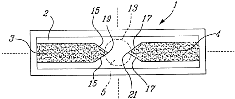
As illustrated in Figure 2, lightly doped region 5 may be disposed roughly
intermediate
60 to, and spacing apart heavily doped regions 3 and 4. Lightly doped region 5
may
be a separate region (with its own dopant concentration, and other
characteristics) spacing apart heavily doped regions 3 and 4, or
alternatively,
may be simply part of substrate 2. Further, lightly doped region 5 may be
CA 02671386 2009-06-08
configured and disposed such that boundary edges 15 and 17 of heavily doped
regions 3 and 4
respectively may be in direct contact with lightly doped region 5. The
boundary edges 15 and 17 are
shown as being a straight line, i.e. in a plane, but it is understood that
said boundary edges 15 and
17 may be curved, inclined etc... The configuration and disposition of heavily
doped regions 3 and
4, as well as that of lightly doped region 5 may encompass a number of
different geometries. For
example, Figure 2 illustrates a configuration wherein heavily doped regions 3
and 4 each have a
pointed tip geometry, wherein the narrow end of each tip 19 and 21
respectively, is pointed towards
the other tip. It is understood however, that since the configuration and
disposition of heavily doped
regions 3 and 4, as well as that of lightly doped region 5 is to be such so as
to allow a better control
of the dopant that migrates from heavily doped regions 3 and 4 into lightly
doped region 5, the
respective geometries of regions 3, 4 and 5 may alternatively, comprise any
number of different
configurations. The respective geometries of regions 3, 4 and 5 may also be
selected to allow for a
better control of the change in the impedance between heavily doped regions 3
and 4.
Turning to figure 3, there is shown a cross sectional view of the tunable
integrated semiconductor
device I as shown in Figures 1 and 2. The application of a focussed heating
pulse 8 (as illustrated
in Figure 1) may have caused a portion of lightly doped region 5, as well as
adjacent portions 19 and
21 of heavily doped regions 3 and 4 respectively (shown in dotted lines), to
melt. The melted areas
may be known as a melted pool 10. In the embodiment illustrated by Figure 3, a
portion of heavily
doped regions 3 and 4 is shown to be included in the melting pool 10. The
extent of heavily doped
regions 3 and 4 which will melt subsequent to the application of the heating
pulse 8 (as shown in
Figure 1) may depend on the characteristics of the heating pulse, namely the
power of the pulse, the
duration of the application of the pulse, the diameter of the pulse, etc...
For example, the diameter
of the heating pulse may encompass a portion of one or both of heavily doped
regions 3 and 4, or
alternatively, the diameter of the focussed heating source may only be wide
enough to encompass
lightly doped region 5. The longer melted pool 10 is melted, the greater the
diffusion of dopant from
heavily doped regions 3 and 4 into lightly doped region 5. However, the amount
of dopants which
will diffuse from heavily doped regions 3 and 4 into lightly doped region 5
may also depend on how
much of heavily doped regions 3 and 4 may be caught by the focussed heating
beam 8, i.e. if a large
21
CA 02671386 2009-06-08
part of heavily doped regions 3 and/or 4 are caused to be melted, more dopants
may diffiise,
and if a small part is caused to be melted, fewer dopants may diffuse.
Depending on the
length of time that melting pool 10 remained melted, the dopant profile across
melted pool 10
from heavily doped region 3 to heavily doped region 4 may not be uniform.
Turning to Figure 4, there is shown a top plan view of the tunable integrated
semiconductor
device 1 following the solidification of the melted pool 10 as shown in Figure
3. As may be
understood, melted pool 10 (of Figure 3) has now been transformed into region
30, which
region 30 has an intermediate dopant concentration, i.e. which dopant
concentration is
intermediate the dopant concentration of heavily doped regions 3 and 4, and
dopant
concentration of lightly doped region 5. As may be understood, since during
the time that the
melted pool 10 was melted, a certain quantity of dopants from heavily doped
region 3 and
heavily doped region 4 were able to diffuse into lightly doped region 5, and
following the
solidification of this melted pool 10, intermediate region 30 may now have a
different dopant
concentration from either of heavily doped region 3, heavily doped region 4,
or lightly doped
region 5. As may be seen, intermediate doped region 30 is roughly a circle in
shape, which
roughly mirrors the shape of the selected area 13 of Figure 2 where the
focussed heating
source was applied.
Turning to Figure 5 there is shown a top plan view of the tunable integrated
semiconductor
device of Figure 4 showing a further steps in the method in accordance with an
embodiment
of the present invention. As may be seen, intermediate doped region 30 is
superimposed by a
further selected area 13, which selected area 13 is subject to a further
application of a
focussed heating pulse 8 as shown in Figure 1. As may be understood, the
application of
focussed heating source 8 may cause most, if not all, of intermediate doped
region 30 to melt,
and further, portions of heavily doped regions 3 and 4 and portions of lightly
doped region 5
may also be caused to melt. This new round of melting may incur further
diffusion of
dopants from the now melted areas of heavily doped regions 3 and 4, into
intermediate doped
region 30. Following the solidification of intermediate doped region 30, the
dopant
concentration of intermediate doped region 30 will be different from the
dopant
concentration of heavily doped region 3, heavily doped 4, and lightly doped
region 5, and will
22
CA 02671386 2009-06-08
further be of a different dopant concentration than the intermediate doped
region 30 as previously
shown in Figure 4.
As may be understood, the iterative method steps shown in Figures 1 to 5 may
be repeated any
number of required or desired times in order to achieve the final required or
desired dopant profile
in intermediate doped region 30. Thus if a high dopant concentration is
required in intermediate
region 30, the iterative steps may be repeated a number of times, for an
example 5 to 15 times, such
that a maximum amount of control diffusion can occur. Conversely, if a low
dopant concentration
is required in intermediate doped region 30, the iterative steps as described
in Figures 1 to 5 may be
performed, for example, only once or twice, and therefore the impedance of
intermediate doped
region 30 may be high, and the dopant concentration may be low in comparison
to the dopant
concentration of heavily doped regions 3 and 4.
Turning now to Figure 6, there is shown a top plan view of a further step in
the method of selectively
tuning the impedance of an integrated semiconductor device. Selectively tuning
the impedance of
an integrated semiconductor device is understood to mean that the impedance
may be increased, or
may be decreased, depending on the requirements of the application. For
example, if in accordance
with an embodiment of the present invention, the impedance of an integrated
semiconductor device
is decrease past the target figure, it is possible to increase the impedance
thereof in order to bring it
into line with what is required. Figure 6 for example illustrates this
particular embodiment in
accordance with the present invention wherein the impedance, after having been
modified in one
direction, (i.e. after the impedance of the integrated semiconductor device
has been decreased
through the method steps illustrated in Figures 1 to 5), it is now required
that the impedance of the
integrated semiconductor device be increased. This may be as a result of the
impedance having been
lowered too much through the previous iterative method steps as illustrated in
Figures 1 to 5, i.e.
wherein the desired final impedance has been overshot, and it is now required
to increase the
impedance of the device.
The method illustrated in Figure 6 may alternatively serve to modify (i.e,
increase) the impedance
23
CA 02671386 2009-06-08
of an integrated semiconductor device independently of the method steps
illustrated in Figures 1 to
5. For example, if once an integrated semiconductor device is in service, it
is determined that said
device may need to be modified to suit a new or different application, the
method illustrated in
Figure 6 may be used to increase the impedance thereof.
The integrated semiconductor illustrate in Figure 6 therefore may comprise
heavily doped regions
3 and 4 and lightly doped regions 5 and 2. In addition, intermediate doped
region 30 may be
disposed spacing apart heavily doped regions 3 and 4 and is further abutting
each of said heavily
doped regions 3 and 4. Intermediate doped region 30, may have a dopant
concentration that is lower
than the concentration of either of the heavily doped regions 3 and 4. In any
event, the dopant
concentration of intermediate doped region 30 may be greater than the dopant
concentration of
lightly doped regions 2 and 5. Thus, in accordance with a particular
embodiment of the present
invention, if it is desired or required to increase the impedance of
intermediate doped region 30 this
may be accomplished by creating the conditions necessary for dopants to
diffuse from intermediate
doped region 30 into lightly doped regions 2 or 5. By accomplishing this
transfer of dopants out of
intennediate doped region 30, the electrical current carrying capacity of
intermediate region 30 may
therefore be reduced, thus increasing the impedance between heavily doped
regions 3 and 4.
Therefore, in order to accomplish this particular embodiment of the present
invention, a focussed
heat source may be trained upon the integrated semiconductor devices such that
said focus heating
source may cover some or all of the intermediate doped region 30 and an
immediately adjacent
region of lightly doped region 5 or 2, said region being a selected area
designated by reference
number 35. Thus as may be understood, the application of a focussed heating
source 8 (as shown
in figure 1) may cause the melting of all or a portion of selected area 35,
which may comprise all
or a portion of intermediate doped region 30 and at the same time cause the
melting of an
immediately adjacent region of lightly doped regions 2 (or 5). During this
time where selected area
is melted, the dopants present in intermediate doped region 30 (which
concentration is higher than
the concentration of the dopants in lightly doped region 2) may, through the
well known and
understood process of diffusion, diffuse from the intermediate doped region 30
into lightly doped
24
CA 02671386 2009-06-08
region 5. The result will be a net lost of dopants from the intermediate doped
region 30 into the
lightly doped region 5, therefore reducing the number of dopants available in
the intermediate doped
region 30 to carry an electric charge therethrough. It is understood that in
accordance with this
particular embodiment of the present invention, the selected area 35 may
preferably not include a
portion of either of highly doped regions 3 and 4.
Once theses steps as described above as been accomplished, and the diffusion
of dopants has
occurred from intermediate doped region 30 to lightly doped region 5, the
impedance of the
integrated semiconductor device may be tested in order to determine whether
sufficient diffusion of
dopants away from intermediate doped region 30 has occurred. If it is
determine that the impedance
has not been modified a require or desired amount, the iterative steps
described above may be
repeated such that further dopants from the intermediate doped region 30 may
be made to diffuse
away from said intermediate doped region 30 into lightly doped region 5.
Alternatively, if
subsequent to the testing of the device it is determined that too much dopant
has diffused from
intermediate doped region 30 into lightly doped region 5, i.e. that the
impedance of the integrated
senliconductor device is now too high and it is now wish to reduce said
impedance, the steps as
illustrated in Figures 1 to 5 may be repeated.
Tunling to Figures 7 and 8 there is shown a top plan view of an alternative
embodiment of the
tunable integrated semiconductor device 1 of the present invention. In
particular, as illustrated in
Figures 7, heavily doped regions 3 and 4 are shown as each having a notched
configuration pointing
towards the other. In accordance with this configuration, the melted pool 16
which will occur as a
result of the application of a focus heating source 8 (as shown in Figure 1)
may encompass more
areas of heavily doped regions 3 and/or 4 and therefore may allow for a faster
and more controlled
diffusion of dopants from heavily doped regions 3 and 4 into lightly doped
region 5. Further, the
device as shown in Figure 7 may facilitate the creation of devices having a
symmetrical dopant
distribution characteristics. As also illustrated in Figure 8, there is shown
a further alternative
configuration of the integrated semiconductor device wherein heavily doped
region 3 comprises a
pointed arrow configuration and heavily doped region 4 comprises a notched
configuration.
CA 02671386 2009-06-08
Turning to Figure 9 there is shown alternative configuration of a turrable
integrated semiconductor
device 1. In accordance with this particular embodiment of the present
invention, the device
comprises first principal tuning arm 50 second principal tuning arm 51 third
secondary tuning arm
54 and fourth secondary tuning arm 55. Spacing apart first and second
principal tuning arms 50 and
51 is a lightly doped region 52; spacing apart third and fourth secondary
tuning arms 54 and 55 is
a further lightly doped region 53 which lightly doped region 53 and lightly
doped region 52 may be
of different size and configuration. Thus in accordance with this particular
embodiment, the
difference between the dopant concentration of lightly doped regions 52 and
the dopant
concentration of first and second principal tuning arms 50 and 51 is such that
no electrical current
may flow therethrough; further, the difference between the dopant
concentration of lightly doped
region 53 and the dopant concentration of third and forth secondary tuning
arms 54 and 55 may be
such that no electrical current may flow therethrough.
As may be seen from the illustration of Figure 9, this particular embodiment
comprises different
sized tuning arms, and therefore, different capacity for carrying electrical
current. As may be
understood, the principal tuning arms 50 and 51 may be used as gross tuning
arms and the third and
forth secondary tuning arms 54 and 55 may be used as fine tuning arms. The
expression fine tuning
is understood to mean that (very) precise impedance changes may be achieved
thereby. It is further
understood that in addition to secondary tuning arms 54 and 55, there may also
be one or more
additional pairs of secondary tuning arms (not shown), which each additional
pair of secondary
tuning arms may further increase the precision tuning capability of the
integrated semiconductor
device. Thus for example, if a large change in the impedance of the integrated
semiconductor device
is required, there may applied a focussed heating source in region 59, as more
fully described above.
As a result of the diffusion of the dopants from heavily doped regions of the
principal tuning arms
50 and 51 respectively, the impedance across first and second principal tuning
arms 50 and 51 may
be modified in accordance with the iterative method as described above. If,
after testing of the
resulting impedance, it is determined that a further adjustment ofthe
impedance across the integrated
semiconductor device is required, a further application of a heating pulse may
be made to region 52,
i.e. either with the same characteristics of the heating pulse (i.e. power,
duration of application,
26
CA 02671386 2009-06-08
etc...), or with different characteristics.
Alternatively, rather then applying a further laser pulse to region 52, the
option exists to apply a
focussed heating source to region 58. This heating pulse may have the same
characteristics as the
pules(s) applied to region 52, or may have different characteristics. Seeing
that third and fourth
secondary tuning arms 54 and 55 are much smaller then the principal tuning
arms 50 and 51, the
quantity of dopants which may be made to diffuse into lightly doped region 58
may be smaller, thus
allowing for better controlled diffusion. The combined action of the change of
impedance across
first and second principal tuning arms 50 and 51 and across third and fourth
secondary tuning arms
54 and 55 is such that the resulting overall changing in the impedance across
the integrated
semiconductor device may be more accurately controlled. As may further be
seen, the integrated
semiconductor device furhter comprises serial resistors 59a and 59b.
As illustrated in Figure 10, there is shown an electric schematic drawing of
the integrated
senliconductor device as illustrated in Figure 9. Reference number 60
represents the main or gross
tuning arm, while reference number 61 depicts the fine tuning arm. Reference
numbers 63 and 64
represent conventional serial integrated resistors 20 and 21 may be added to
the integrated device
which may linlit voltage on tunable part of the integrated semiconductor
device, the whole in order
to obtain high impedance devices, and may make the device exhibit linear
current/voltage
cliaracteristics.
Turning to Figures 11 and 12 there is illustrated a representation of a
general embodiment of an
apparatus 100 for modifying the impedance of an integrated semiconductor
device using a focussed
heating source, such as a laser. An integrated circuit 110 is placed on a
positioning table 10, and may
be subjected to an application of a heating source 105 which is produced by a
focussed heating
source 103. Heating source 105 may be focussed on integrated circuit 110 by
using optic or magnetic
lenses 107, and a system of cameras and mirrors allows for the observation of
the integrated circuit
110 in order to ensure accurate alignment of the heating source 105. Figure 12
shows apparatus 100
in greater detail. Laser 103 is connected to shutter 116, each of which is
controlled by the control
27
CA 02671386 2009-06-08
system shown as computer 108. Also connected to computer 108 is4he control
mechanism 109 of
the positioners 101. The apparatus 100further comprises a camera 112, and a
light source 114. A
further component of the apparatus 100 is a beam splitter 113, and a selective
mirror 120.
Turning to Figure 13, there is shown a chart illustrating an example of the
number of applications
required to obtain a given resistance across an integrated semiconductor
device. The chart illustrates
some of the various characteristics of a focussed heating source which may be
varied during the
iterative steps. Column 1 indicates the number of applications of a focussed
heating source, column
2 represents the power in milliwatt of the focussed heating source, column 3
indicates the duration
of the application of the focussed heating source (in micro seconds), column 4
shows the diameter
of the focussed heating source in micro metres, and the last column is the
attained resistance across
the example integrated semiconductor device. For example, the first
application comprises a
focussed heating source of a power of 1400 milliwatt, applied for 1.4
microseconds, and having a
focussed beam source diameter of 4 micro metres. The resulting resistance is
188.9 ohms. A second
application having identical characteristics was applied wherein the
resistance of the integrated
semiconductor devices dropped 148.6 ohms. By the third application, the power
of the laser
application remained unchanged, yet the duration of the application was
reduced from 1.4
microseconds to 0.96 microseconds, with a resulting resistance of 142.8 ohms.
By the fourth
application, the power was unchanged but the duration of the application
dropped to 0.48
microseconds and the resulting resistance was down to 141.4 microseconds. For
the fifth
application, the power was reduced to 200 milliwatt, the duration of the
application remained at 0.48
microseconds and the resistance value dropped to 140.1 ohm. Finally, for the
6th and last
application, the characteristics of the focussed heating source remained
unchanged and the resistance
dropped to 140.0 ohm. As may be seen, the last iteration in accordance with
the embodiment of the
present invention, caused a change of 0.1 ohm in the impedance of the device,
which can be
considered to be very fine tuning of the device.
As can be seen from the table illustrated at Figure 13, the iterative process
of a particular
embodiment of the present invention has progressively dropped the resistance
across the integrated
28
CA 02671386 2009-06-08
semiconductor device, throughthe application of a number of pulse from a
focussed heating source,
wherein the characteristics of the heating pulse were modified, as required in
order to effect a
progressively closer result to the final desired result.
Turning to Figure 14 there is illustrated a current voltage curve of a tunable
integrated semiconductor
device having a low resistance value. In order to obtain integrated
semiconductor devices with the
required precise impedance characteristics, a very precise control of dopant
diffusion into lightly
doped region 5 (as shown by reference number 5 in Figures 1 to5) may be
necessary. For example,
if an integrated semiconductor device of low or very low impedance (i.e.
resistance) is required, the
controlled diffusion in accordance with an embodiment of the present invention
may require a
significant amount of dopants to diffuse into lightly doped region 5 from
heavily doped region 3 and
4. The end result in accordance with this embodiment may be, for example, to
create a quasi-uniform
dopants distribution from heavily doped region 3, across (formerly lightly)
doped region 5 and
through heavily doped region 4 as shown in Figures 1-5. In such situation,
voltage/current curve of
the tuned integrated semiconductor device may show excellent linearity as
illustrated in Figure 14.
Alternatively, applications may call for a high impedance (i.e. resistance)
device, which may be
obtained by controlled diffusion of a small or minimum amount of dopant into
lightly doped region
5 from heavily doped region 3 and 4. As a result, in accordance with this
embodiment, there may
be a non-uniform distribution ofdopant in the lightly doped region 5 between
heavily doped regions
3 and 4. It is known that non-uniform doping in semiconductor devices creates
non-linear
phenomena. In such a situation, voltage/current curve of the tuned integrated
semiconductor device
niay show strong non-linear characteristics as depicted in Figure 15.
To solve this problem and to obtain high impedance devices, conventional
serial integrated resistors
20 and 21 may be added which may limit voltage on tunable part of the
integrated semiconductor
device and may make it work in the linear region of the Figure 15, as
illustrated in Figure 16.
Figure 16 illustrates a current voltage curve for an integrated semiconductor
device similar to that
29
CA 02671386 2009-06-08
S shown in Figure 15, but wherein the integrated semiconductor device further
comprises serial
resistors 59a and 59b. This has the effect of creating a linear current
voltage curve of the apparatus.