Note: Descriptions are shown in the official language in which they were submitted.
CA 02672259 2009-06-10
DESCRIPTION
Method of Manufacturing Semiconductor Device
TECHNICAL FIELD
The present invention relates to a method of manufacturing a semiconductor
device, and particularly to a method of manufacturing a semiconductor device
that
allows the senuconductor device to be reduced in size and also allows
variations in
characteristics of the semiconductor device to be reduced.
BACKGROUND ART
An MOSFET (Metal Oxide Semiconductor Field Effect Transistor; hereinafter
also referred to as an "SiC-MOSFET") which includes SiC (silicon carbide) and
is a type
of a semiconductor device is fabricated through the process roughly divided
into
selective ion implantation, activation annealing, gate oxide film formation,
and electrode
formation.
Referring to schematic cross-sectional views in Figs. 20-30, an example of a
conventional method of manufacturing an SiC-MOSFET will be hereinafter
described.
First, as shown in Fig. 20, an n-type SiC film 202 is epitaxially grown on the
surface of an SiC substrate 201. As shown in Fig. 21, an ion implantation mask
203 is
then formed on the entire surface of SiC film 202.
Then, as shown in Fig. 22, a resist 204 having a predetermined opening 205 is
formed on ion implantation mask 203 using the photolithography technique. As
shown
in Fig. 23, the portion of ion implantation mask 203 located under opening 205
is
removed by etching to expose a portion of the surface of SiC film 202.
Then, as shown in Fig. 24, resist 204 is removed and ions of an n-type dopant
such as phosphorus are ion-implanted into the exposed surface of SiC film 202
to
thereby form an n-type dopant implantation region 206 on the surface of SiC
film 202.
Then, as shown in Fig. 25, ion implantation mask 203 is entirely removed from
- I -
CA 02672259 2009-06-10
the surface of SiC film 202. As shown in Fig. 26, ion implantation mask 203 is
again
formed on the entire surface of SiC film 202.
As shown in Fig. 27, resist 204 is partially formed on the surface of ion
implantation mask 203 using the photolithography technique, in which resist
204 may be
formed at the position displaced from the specified position depending on the
accuracy
of a photolithography apparatus, and the like.
Then, as shown in Fig. 28, a portion of ion implantation mask 203 in which
resist
204 is not formed is removed by etching to thereby expose a portion of the
surface of
SiC film 202.
Then, as shown in Fig. 29, ions of a p-type dopant such as aluminum are ion-
implanted into the exposed surface of SiC film 202 to thereby form a p-type
dopant
implantation region 207 on the surface of SiC film 202.
Ion implantation mask 203 and resist 204 are then removed and the activation
annealing is carried out for restoring crystallinity of the wafer from which
ion
implantation mask 203 and resist 204 have been removed.
As shown in Fig. 30, a gate oxide film 208, a source electrode 209 and a drain
electrode 211 are formed on the surface of SiC film 202, and a gate electrode
210 is
formed on the surface of gate oxide film 208. Then, wiring is provided to each
of
source electrode 209, gate electrode 210 and drain electrode 211, and the
wafer is
divided into chips to thereby complete an SiC-MOSFET.
Non-Patent Document 1: Hiroyuki Matsunami (write and edit), "Semiconductor SiC
Technology and Applications", Nikkan Kogyo Shimbun-sha, March in 2003
DISCLOSURE OF THE INVENTION
PROBLEMS TO BE SOLVED BY THE INVENTION
Since a diffusion coefficient of a dopant is small in SiC, the n-type dopant
and
the p-type dopant each are introduced not by the diffusion method but by the
ion
implantation method.
However, as described above, the position where the resist to be used as an
ion
-2-
CA 02672259 2009-06-10
implantation mask for the implantation of the ions of the n-type dopant and
the p-type
dopant is formed varies depending on the accuracy of the photolithography
apparatus,
and the like. This causes a problem that variations occur in the relative
positional
relationship between the n-type dopant implantation region and the p-type
dopant
implantation region, with the result that variations occur in the gate length
of the SiC-
MOSFET to cause variations in characteristics of the SiC-MOSFET. Furthermore,
it
is also desired that the semiconductor device be further reduced in size.
An object of the present invention is to provide a method of manufacturing a
semiconductor device that allows the semiconductor device to be reduced in
size and
also allows variations in characteristics of the semiconductor device to be
reduced.
MEANS FOR SOLVING THE PROBLEMS
The present invention provides a method of manufacturing a semiconductor
device including a first step of forming an ion implantation mask on a portion
of the
surface of a semiconductor; a second step of implanting ions of a first dopant
into at
least a portion of an exposed region of the surface of the semiconductor other
than the
region where the ion implantation mask is formed, to form a first dopant
implantation
region; a third step of, after forming the first dopant implantation region,
removing a
portion of the ion implantation mask to increase the exposed region of the
surface of the
semiconductor; and a fourth step of implanting ions of a second dopant into at
least a
portion of the increased exposed region of the surface of the semiconductor to
form a
second dopant implantation region.
According to the method of manufacturing the semiconductor device of the
present invention, the ion implantation mask used for forming the first dopant
implantation region can also be used for forming the second dopant
implantation region,
and the variation in the relative positional relationship between the first
dopant
implantation region and the second dopant implantation region can be reduced.
This
allows the semiconductor device to be reduced in size and also allows
variations in
characteristics of the semiconductor device to be reduced. Furthermore,
according to
-3-
CA 02672259 2009-06-10
the method of manufacturing the semiconductor device of the present invention,
since
only a single formation of the resist for patterning the ion implantation mask
is required,
the number of steps can also be reduced as compared to the conventional case.
Furthermore, in the method of manufacturing the semiconductor device of the
present invention, it is preferable that the ion implantation mask includes at
least one
selected from a group consisting of tungsten, silicon, aluminum, nickel, and
titanium.
In this case, the ion implantation mask serves as a mask for the implantation
of the ions
of the first dopant and the second dopant, and can include an adhesion
improving layer
improving adhesion to the semiconductor surface and an etching stop layer
allowing the
etching on the semiconductor surface to be suppressed. The above-mentioned
tungsten, silicon, aluminum, nickel, and titanium may each be contained in the
ion
implantation mask singly or may be contained in the ion implantation mask in
the form
of a compound.
Furthermore, in the method of manufacturing the semiconductor device of the
present invention, the ion implantation mask may be formed of two or more
layers. In
the case where the ion implantation mask is formed of two or more layers, when
a
portion of the ion implantation mask is removed after the formation of the
first dopant
implantation region to increase the exposed region of the surface of the
semiconductor,
the ion implantation mask can be reduced in width while suppressing the
reduction in
thickness thereof. Consequently, the reliability of the ion implantation mask
at the time
of the implantation of the ions of the second dopant is improved.
Furthermore, in the method of manufacturing the semiconductor device of the
present invention, the ion implantation mask may be formed of two layers
including a
first ion implantation mask and a second ion implantation mask formed on the
first ion
implantation mask. In this case, when a portion of the first ion implantation
mask is
removed after the formation of the first dopant implantation region to
increase the
exposed region of the surface of the semiconductor, the first ion implantation
mask can
be reduced in width while suppressing the reduction in thickness of the first
ion
-4-
CA 02672259 2009-06-10
implantation mask. Consequently, the reliability of the first ion implantation
mask at
the time of the implantation of the ions of the second dopant is improved.
Furthermore, in the above description, it is preferable that the first ion
implantation mask contains tungsten as a main component and the second ion
implantation mask contains silicon oxide as a main component. In this case,
there is a
significant tendency that the second ion implantation mask is resistant to
etching during
the etching of the first ion implantation mask and the first ion implantation
mask is
resistant to etching during the etching of the second ion implantation mask,
and thus, the
first ion implantation mask can be reduced in width while suppressing the
reduction in
thickness of the first ion implantation mask. Consequently, the reliability of
the first
ion implantation mask at the time of the implantation of the ions of the
second dopant is
improved.
Furthermore, in the method of manufacturing the semiconductor device of the
present invention, the first step may be performed by stacking the first ion
implantation
mask and the second ion implantation mask in this order on the surface of the
semiconductor to form the ion implantation mask, and subsequently, etching a
portion of
the ion implantation mask to thereby expose a portion of the surface of the
semiconductor; the third step may be performed by, after forming the first
dopant
implantation region, etching the first ion implantation mask at least in its
width direction;
a step of removing the second ion implantation mask by etching may be included
between the third step and the fourth step; and, a step of removing the first
ion
implantation mask by etching may be included after the fourth step. In this
case, while
reduction in size of the semiconductor device and reduction in variations in
characteristics of the semiconductor device can be achieved, the number of
steps can
also be reduced as compared to the conventional case.
Furthermore, in the method of manufacturing the semiconductor device of the
present invention, it is preferable that the selective ratio of the second ion
implantation
mask to the first ion implantation mask by an etching solution or etching gas
for etching
-5-
CA 02672259 2009-06-10
the second ion implantation mask is not less than 2. In this case, before
implanting the
ions of the second dopant, the etching of the second ion implantation mask can
be
suppressed and the first ion implantation mask can be etched in its width
direction while
suppressing the reduction in thickness of the first ion implantation mask.
Consequently,
the reliability of the first ion implantation mask at the time of the
implantation of the ions
of the second dopant is improved.
Furthermore, in the method of manufacturing the semiconductor device of the
present invention, it is preferable that the etching in the first step and the
etching in the
third step each are performed by dry etching. In this case, in the first step
in which the
surface of the semiconductor is exposed, the etching tends to proceed in the
thickness
direction of each of the first ion implantation mask and the second ion
implantation mask,
and in the third step in which the exposed region of the surface of the
semiconductor is
increased, the etching in the width direction of each of the first ion
implantation mask
and the second ion implantation mask tends to be readily controlled.
Accordingly, the
first ion implantation mask and the second ion implantation mask can each be
prevented
from being needlessly etched during the etching of each of these ion
implantation masks.
Furthermore, in the method of manufacturing the semiconductor device of the
present invention, it is possible that the portion of the ion implantation
mask is removed
by etching in the third step and the ion implantation mask after the etching
in the third
step has a thickness serving as an implantation mask for the ions of the
second dopant in
the fourth step. In this case, the ion implantation mask serves as an
implantation mask
for the ions of the second dopant, which can prevent the second dopant
implantation
region from being formed in the portion where the second dopant implantation
region is
not required.
Furthermore, in the method of manufacturing the semiconductor device of the
present invention, the ion implantation mask may contain tungsten as a main
component.
The ion implantation mask containing tungsten as a main component is
preferable in that
tungsten is a high density material and is highly capable of preventing the
ion
-6-
CA 02672259 2009-06-10
implantation, which allows the ion implantation mask to be formed thinner than
in the
case of other materials, with the result that the process tends to be
simplified.
Furthermore, in the method of manufacturing the semiconductor device of the
present invention, the first step may be performed by, after forming the ion
implantation
mask on the surface of the semiconductor, etching a portion of the ion
implantation
mask to thereby expose a portion of the surface of the semiconductor; the
third step may
be performed by, after forming the first dopant implantation region, etching
the ion
implantatiori mask at least in its width direction; and, a step of removing
the ion
implantation mask may be included after the fourth step. In this case, while
reduction
in size of the semiconductor device and reduction in variations in
characteristics of the
semiconductor device can be achieved, the number of steps can also be reduced
as
compared to the conventional case.
It is preferable that the etching in the first step and the etching in the
third step
each are performed by dry etching. In this case, in the first step in which
the surface of
the semiconductor is exposed, the etching tends to proceed in the thickness
direction of
the ion implantation mask, and in the third step in which the exposed region
of the
surface of the semiconductor is increased, the etching in the width direction
of the ion
implantation mask tends to be readily controlled. Accordingly, the ion
implantation
mask can be prevented from being needlessly etched during the etching of the
ion
implantation mask.
Furthermore, in the method of manufacturing the semiconductor device of the
present invention, it is preferable that the senuconductor has a band gap
energy of not
less than 2.5 eV. This tends to allow the manufacture of the semiconductor
device that
withstands a high voltage, achieves loss low, and is excellent in heat
resistance and
environment resistance.
Furthermore, in the method of manufacturing the semiconductor device of the
present invention, it is preferable that the semiconductor contains silicon
carbide as a
main component. In the semiconductor device made of silicon carbide, since the
-7-
CA 02672259 2009-06-10
activation annealing temperature becomes high after the dopant implantation,
the self-
alignment method as in the conventional Si device cannot be used, and thus,
the present
invention can be particularly suitably used.
EFFECTS OF THE INVENTION
According to the present invention, a method of manufacturing a semiconductor
device can be provided that allows the semiconductor device to be reduced in
size and
also allows variations in characteristics of the semiconductor device to be
reduced.
BRIEF DESCRIPTION OF THE DRAWINGS
Fig. I is a schematic cross-sectional view showing a part of an example of a
method of manufacturing a semiconductor device of the present invention.
Fig. 2 is a schematic cross-sectional view showing a part of the example of
the
method of manufacturing the semiconductor device of the present invention.
Fig. 3 is a schematic cross-sectional view showing a part of the example of
the
method of manufacturing the semiconductor device of the present invention.
Fig. 4 is a schematic cross-sectional view showing a part of the example of
the
method of manufacturing the semiconductor device of the present invention.
Fig. 5 is a schematic cross-sectional view showing a part of the example of
the
method of manufacturing the semiconductor device of the present invention.
Fig. 6 is a schematic cross-sectional view showing a part of the example of
the
method of manufacturing the semiconductor device of the present invention.
Fig. 7 is a schematic cross-sectional view showing a part of the example of
the
method of manufacturing the semiconductor device of the present invention.
Fig. 8 is a schematic cross-sectional view showing a part of the example of
the
method of manufacturing the semiconductor device of the present invention.
Fig. 9 is a schematic cross-sectional view showing a part of the example of
the
method of manufacturing the semiconductor device of the present invention.
Fig. 10 is a schematic cross-sectional view showing a part of the example of
the
method of manufacturing the semiconductor device of the present invention.
-8-
CA 02672259 2009-06-10
Fig. 11 is a schematic cross-sectional view showing a part of another example
of
the method of manufacturing the semiconductor device of the present invention.
Fig. 12 is a schematic cross-sectional view showing a part of another example
of
the method of manufacturing the semiconductor device of the present invention.
Fig. 13 is a schematic cross-sectional view showing a part of another example
of
the method of manufacturing the semiconductor device of the present invention.
Fig. 14 is a schematic cross-sectional view showing a part of another example
of
the method of manufacturing the semiconductor device of the present invention.
Fig. 15 is a schematic cross-sectional view showing a part of another example
of
the method of manufacturing the semiconductor device of the present invention.
Fig. 16 is a schematic cross-sectional view showing a part of another example
of
the method of manufacturing the semiconductor device of the present invention.
Fig. 17 is a schematic cross-sectional view showing a part of another example
of
the method of manufacturing the semiconductor device of the present invention.
Fig. 18 is a schematic cross-sectional view showing a part of another example
of
the method of manufacturing the semiconductor device of the present invention.
Fig. 19 is a schematic cross-sectional view showing a part of another example
of
the method of manufacturing the semiconductor device of the present invention.
Fig. 20 is a schematic cross-sectional view showing a part of an example of a
method of manufacturing a conventional SiC-MOSFET.
Fig. 21 is a schematic cross-sectional view showing a part of the example of
the
method of manufacturing the conventional SiC-MOSFET.
Fig. 22 is a schematic cross-sectional view showing a part of the example of
the
method of manufacturing the conventional SiC-MOSFET.
Fig. 23 is a schematic cross-sectional view showing a part of the example of
the
method of manufacturing the conventional SiC-MOSFET.
Fig. 24 is a schematic cross-sectional view showing a part of the example of
the
method of manufacturing the conventional SiC-MOSFET.
-9-
CA 02672259 2009-06-10
Fig. 25 is a schematic cross-sectional view showing a part of the example of
the
method of manufacturing the conventional SiC-MOSFET.
Fig. 26 is a schematic cross-sectional view showing a part of the example of
the
method of manufacturing the conventional SiC-MOSFET.
Fig. 27 is a schematic cross-sectional view showing a part of the example of
the
method of manufacturing the conventional SiC-MOSFET.
Fig. 28 is a schematic cross-sectional view showing a part of the example of
the
method of manufacturing the conventional SiC-MOSFET.
Fig. 29 is a schematic cross-sectional view showing a part of the example of
the
method of manufacturing the conventional SiC-MOSFET.
Fig. 30 is a schematic cross-sectional view showing a part of the example of
the
method of manufacturing the conventional SiC-MOSFET.
DESCRIPTION OF THE REFERENCE SIGNS
101, 201 SiC substrate, 102, 202 SiC film, 103, 203 ion implantation mask,
103a
first ion implantation mask, 103b second ion implantation mask, 104, 204
resist, 105,
205 opening, 106, 206 n-type dopant implantation region, 107, 207 p-type
dopant
implantation region, 108, 208 gate oxide film, 109, 209 source electrode, 110,
210 gate
electrode, 111, 211 drain electrode.
BEST MODES FOR CARRYING OUT THE INVENTION
The embodiments of the present invention will be hereinafter described. In the
accompanying drawings of the present invention, the same or corresponding
components are designated by the same reference characters.
(First Embodiment)
Referring to the schematic cross-sectional views in Figs. 1-10, an example of
the
method of manufacturing the semiconductor device of the present invention will
be
hereinafter described.
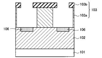
First, as shown in Fig. 1, an n-type SiC film 102 is epitaxially grown on the
surface of an SiC substrate 101 to form a wafer. Then, as shown in Fig. 2, a
first ion
- 10-
CA 02672259 2009-06-10
implantation mask 103 a made of tungsten is formed on the entire surface of
SiC film 102,
and, on the surface of first ion implantation mask 103a, a second ion
implantation mask
103b made of silicon oxide is formed, with the result that an ion implantation
mask 103
made of a stacked body including first ion implantation mask 103a and second
ion
implantation mask 103b is formed.
First ion implantation mask 103a made of tungsten and second ion implantation
mask 103b made of silicon oxide each can be formed by, for example, the
sputtering
method, the CVD (Chemical Vapor Deposition) method, or the like.
Furthermore, it is preferable that first ion implantation mask 103a made of
tungsten is formed to have a thickness of not more than 2 m, and more
preferably a
thickness of not more than 1 m. It is also preferable that second ion
implantation
mask 103b made of silicon oxide is formed to have a thickness of not more than
0.5 m,
and more preferably a thickness of not more than 0.3 m.
As shown in Fig. 3, a resist 104 having a predetermined opening 105 is then
formed on second ion implantation mask 103b using, for example, the
photolithography
technique. Then, as shown in Fig. 4, a portion of each of first ion
implantation mask
103a and second ion implantation mask 103b located under opening 105 is
removed in
the thickness direction by etching, to expose a portion of the surface of SiC
film 102.
As shown in Fig. 5, resist 104 is then removed and ions of an n-type dopant
such
as phosphorus are ion-implanted into the exposed surface of SiC film 102 to
thereby
form an n-type dopant implantation region 106 on the surface of SiC film 102.
As shown in Fig. 6, first ion implantation mask 103a is etched in its width
direction to decrease the width of first ion implantation mask 103a. This
causes
exposure of the region of the surface of SiC film 102 other than the region
where n-type
dopant implantation region 106 is formed, to increase the exposed region of
the surface
of SiC film 102.
The material used as an etching solution or etching gas for etching first ion
implantation mask 103a has a property in which first ion implantation mask
103a is
-11-
CA 02672259 2009-06-10
etched more readily than in the case of second ion implantation mask 103b.
Then, as shown in Fig. 7, second ion implantation mask 103b on first ion
implantation mask 103a is removed by etching. The material used as the etching
solution or etching gas for etching second ion implantation mask 103b has a
property in
which second ion implantation mask 103b is etched more readily than in the
case of first
ion implantation mask 103a.
As shown in Fig. 8, ions of a p-type dopant such as aluminum are ion-implanted
into the thus increased exposed region of the surface of SiC film 102, to
thereby form a
p-type dopant implantation region 107 on the surface of SiC film 102.
As shown in Fig. 9, first ion implantation mask 103a is removed. Then, the
activation annealing is carried out for restoring crystallinity of the wafer
from which first
ion implantation mask 103a has been removed and also activating the ions of
the ion-
implanted n-type dopant and p-type dopant.
As shown in Fig. 10, after a gate oxide film 108, a source electrode 109 and a
drain electrode 111 are formed on the surface of SiC film 102 and a gate
electrode 110
is formed on the surface of gate oxide film 108, the wafer is divided into
chips to
thereby complete an SiC-MOSFET.
Thus, in the present embodiment, the ion implantation mask used for forming
the
n-type dopant implantation region can also be used for forming the p-type
dopant
implantation region. This eliminates the need to separately form the ion
implantation
mask for forming the n-type dopant implantation region and the ion
implantation mask
for forming the p-type dopant implantation region as in the conventional case.
Therefore, as compared to the conventional case, it is possible to reduce the
variation in the relative positional relationship between the n-type dopant
implantation
region and the p-type dopant implantation region and to shorten the gate
length, which
leads to reduction in size of the semiconductor device. The reduction in the
variation
also allows variations in characteristics of the semiconductor device to be
reduced.
Furthermore, since only a single formation of the resist for patterning the
ion
-12-
CA 02672259 2009-06-10
implantation mask is required, the number of steps can also be reduced as
compared to
the conventional case.
Ion implantation mask 103 may include the layer made of, for example,
titanium,
nickel, silicon oxide, or silicon nitride between first ion implantation mask
103a made of
tungsten and the surface of SiC film 102. This layer is provided because it
may
improve the adhesion between ion implantation mask 103 and SiC film 102 and
may also
serve as an etching stop layer of the surface of SiC film 102. This layer can
be formed,
for example, to have a thickness of not more than 100 nm.
In the above description, although tungsten is used for first ion implantation
mask 103a and silicon oxide is used for second ion implantation mask 103b, it
goes
without saying that the present invention is not limited thereto. For example,
a silicon
compound such as silicon oxide, silicon nitride or silicon oxynitride can be
used for first
ion implantation mask 103a, and metal such as aluminum or titanium can be used
for
second ion implantation mask 103b.
In other words, the material used for first ion implantation mask 103a may
have
a property that is more resistant to etching by the etching solution or
etching gas for
etching second ion implantation mask 103b than in the case of second ion
implantation
mask 103b. The material used for second ion implantation mask 103b may have a
property that is more resistant to etching by the etching solution or etching
gas for
etching first ion implantation mask 103a than in the case of first ion
implantation mask
103 a.
Particularly, it is preferable to use tungsten for first ion implantation mask
103a
and to use silicon oxide for second ion implantation mask 103b. In this case,
second
ion implantation mask 103b tends to be more resistant to etching during the
etching of
first ion implantation mask 103a, and first ion implantation mask 103a tends
to be more
resistant to etching during the etching of second ion implantation mask 103b.
Thus,
first ion implantation mask 103a can be reduced in width while suppressing the
reduction in thickness of first ion implantation mask 103a. Therefore, the
reliability of
- 13 -
CA 02672259 2009-06-10
` `.
first ion implantation mask 103a at the time of the implantation of the ions
of the second
dopant can be improved.
It is to be noted that, in the present invention, ion implantation mask 103 is
not
limited to the above-described two-layer configuration, but may be one layer
or may be
three or more layers.
Furthermore, it is preferable that the selective ratio of second ion
implantation
mask 103b to first ion implantation mask 103a by the etching solution or
etching gas for
etching second ion implantation mask 103b is not less than 2. In this case,
before
implanting the ions of the p-type dopant, the etching of second ion
implantation mask
103b can be suppressed and first ion implantation mask 103a can be etched in
its width
direction while suppressing the reduction in thickness of first ion
implantation mask
103a. Consequently, the reliability of first ion implantation mask 103a at the
time of
the implantation of the ions of the p-type dopant is improved.
The above-mentioned selective ratio can be calculated by etching first ion
implantation mask 103a and second ion implantation mask 103b by the etching
solution
or etching gas on the same conditions and obtaining the ratio between the
etching rate of
first ion implantation mask 103a and the etching rate of second ion
implantation mask
103b (the etching rate of first ion implantation mask 103a/the etching rate of
second ion
implantation mask 103b).
In the above description, it is preferable that the etching of each of first
ion
implantation mask 103a and second ion implantation mask 103b in the thickness
direction shown in Fig. 4 is carried out by dry etching using etching gas.
Although the
etching of first ion implantation mask 103a in its width direction shown in
Fig. 6 may
also be carried out by wet etching using etching solution, it is preferable
that the etching
is carried out by dry etching using etching gas.
In the case of the dry etching using etching gas, a bias voltage is generally
applied to SiC substrate 101 and the etching gas proceeds with a certain
directivity in
the direction of SiC substrate 101. Accordingly, the etching tends to proceed
in the
-14-
CA 02672259 2009-06-10
thickness direction of each of first ion implantation mask 103 a and second
ion
implantation mask 103b as compared to the case of the wet etching.
Furthermore, in
the case of the wet etching using etching solution, the isotropic etching
tends to proceed,
and therefore, the etching tends to proceed in the width direction of first
ion
implantation mask 103a as compared to the case of the dry etching. However,
for the
purpose of facilitating the etching control, it is preferable to etch first
ion implantation
mask 103a in its width direction by dry etching using etching gas.
In the above description, SiC is used as a semiconductor, but it goes without
saying that a semiconductor other than SiC may be used. In the present
invention, for
example, gallium nitride, diamond, zinc oxide, aluminum nitride, or the like
may be used
as a semiconductor.
Particularly, in the present invention, it is preferable to use a
semiconductor
having a band gap energy of not less than 2.5 eV. This tends to allow the
manufacture
of the semiconductor device that withstands a high voltage, achieves low loss,
and is
excellent in heat resistance and environment resistance.
In the above description, although the case where an SiC-MOSFET is
manufactured as a semiconductor device has been described, it goes without
saying that,
in the present invention, a semiconductor device other than the SiC-MOSFET may
be
manufactured using a semiconductor other than SiC.
Furthermore, it goes without saying that, in the present invention, the above-
described p-type conductivity and n-type conductivity may be replaced with
each other.
(Second Embodiment)
Referring to the schematic cross-sectional views in Figs. 11-19, an example of
the method of manufacturing the semiconductor device of the present invention
will be
hereinafter described.
First, as shown in Fig. 11, n-type SiC film 102 is epitaxially grown on the
surface
of SiC substrate 101 to form a wafer. Then, as shown in Fig. 12, ion
implantation
mask 103 made of tungsten is formed on the entire surface of SiC film 102.
-15-
CA 02672259 2009-06-10
As shown in Fig. 13, resist 104 having predetermined opening 105 is then
formed on the surface of ion implantation mask 103 using, for example, the
photolithography technique. Then, as shown in Fig. 14, a portion of
implantation mask
103 located under opening 105 is removed by etching to expose a portion of the
surface
of SiC film 102.
Then, as shown in Fig. 15, resist 104 is removed and ions of an n-type dopant
such as phosphorus are ion-implanted into the exposed surface of SiC film 102
to
thereby form n-type dopant implantation region 106 on the surface of SiC film
102.
Then, as shown in Fig. 16, ion implantation mask 103 is subjected to isotropic
etching and is removed in its width direction to reduce the width of ion
implantation
mask 103. This causes exposure of the region of the surface of SiC film 102
other than
the region where n-type dopant implantation region 106 is formed, to increase
the
exposed region of the surface of SiC film 102.
In the present embodiment, the above-described isotropic etching causes ion
implantation mask 103 to be entirely etched, with the result that not only the
width but
also the height of ion implantation mask 103 is reduced.
Then, as shown in Fig. 17, the ions of the p-type dopant such as aluminum are
ion-implanted into the thus increased exposed region of the surface of SiC
film 102, to
thereby form p-type dopant implantation region 107 on the surface of SiC film
102.
As shown in Fig. 18, ion implantation mask 103 is removed. Then, the
activation annealing is carried out for restoring crystallinity of the wafer
from which ion
implantation mask 103 has been removed.
As shown in Fig. 19, after gate oxide film 108, source electrode 109 and drain
electrode 111 are formed on the surface of SiC film 102 and gate electrode 110
is
formed on the surface of gate oxide film 108, the wafer is divided into chips
to thereby
complete an SiC-MOSFET.
Thus, in the present embodiment, the ion implantation mask used for forming
the
n-type dopant implantation region can also be used for forming the p-type
dopant
- 16-
CA 02672259 2009-06-10
implantation region. This eliminates the need to separately form the ion
implantation
mask for forming the n-type dopant implantation region and the ion
implantation mask
for forming the p-type dopant implantation region.
Therefore, as compared to the conventional case, it is possible to reduce the
variation in the relative positional relationship between the n-type dopant
implantation
region and the p-type dopant implantation region and to shorten the gate
length, which
leads to reduction in size of the semiconductor device. The reduction in the
variation
also allows variations in characteristics of the semiconductor device to be
reduced.
Furthermore, since only a single formation of the resist for patterning ion
implantation mask 103 is required, the number of steps can also be reduced as
compared
to the conventional case.
In the present embodiment, although tungsten is used for ion implantation mask
103, it goes without saying that the present invention is not limited thereto.
Furthermore, in the above description, it is preferable that ion implantation
mask
103 after the etching shown in Fig. 16 has a thickness that serves as an ion
implantation
mask in the subsequent ion implantation of the ions of the p-type dopant. This
is
because, when ion implantation mask 103 after the etching shown in Fig. 16
does not
serve as an ion implantation mask in the ion implantation described below, p-
type
dopant implantation region 107 is formed in the area where it is not required.
The
thickness serving as an ion implantation mask means a thickness that allows
99.9% or
more of the ion-implanted ions to be prevented from being implanted.
For example, in the case where ion implantation mask 103 is reduced in width
by
x from either side thereof by the etching shown in Fig. 16, ion implantation
mask 103
may be reduced in thickness by x or more. In this case, it is sufficient that
the thickness
of ion implantation mask 103 after reduction by x or more is equal to or
greater than the
thickness serving as an ion implantation mask.
Furthermore, in the above description, it is preferable that the etching of
ion
implantation mask 103 in the thickness direction shown in Fig. 14 is carried
out by dry
-17-
CA 02672259 2009-06-10
=
etching using etching gas. Furthermore, although the etching of ion
implantation mask
103 shown in Fig. 16 may also be carried out by wet etching using etching
solution, it is
preferable that the etching is carried out by dry etching using etching gas.
As described above, in the case of the dry etching using etching gas, the
etching
gas proceeds with a certain directivity in the direction of SiC substrate 101.
Accordingly, the etching tends to proceed in the thickness direction of ion
implantation
mask 103 as compared to the case of the wet etching. Furthermore, in the case
of the
wet etching using etching solution, the isotropic etching tends to proceed,
and therefore,
the etching tends to proceed in the width direction of ion implantation mask
103 as
compared to the case of the dry etching. However, for the purpose of
facilitating the
etching control, it is preferable to etch ion implantation mask 103 in its
width direction
by dry etching using etching gas.
It is to be noted that other descriptions in the present embodiment are the
same
as those in the first embodiment.
Example
(Example 1)
A wafer having an n-type SiC film epitaxially grown on the surface of an SiC
substrate was first prepared, in which the epitaxially grown n-type SiC film
had a film
thickness of 10 m and the n-type dopant had a concentration of 1 x 1015cm 3.
Then, a first ion implantation mask made of tungsten was formed on the entire
surface of the SiC film by the sputtering method, and a second ion
implantation mask
made of silicon oxide was formed on the first ion implantation mask by the
sputtering
method, in which the first ion implantation mask had a thickness of 800 nm and
the
second ion implantation mask had a thickness of 100 nrn.
Then, the photolithography technique was used to form on the second ion
implantation mask a resist patterned so as to have an opening in the portion
of the n-
type dopant implantation region to be formed.
Then, the portion of the second ion implantation mask exposed from the opening
-18-
CA 02672259 2009-06-10
f
of the resist was etched by CF4 gas for removal. The portion of the first ion
implantation mask exposed from the second ion implantation mask removed as
described above was etched by SF6 gas, to expose the surface of the SiC film
located
under the opening of the above-described resist.
CF4 gas was an etching gas by which the second ion implantation mask made of
silicon oxide was etched more than in the case of the first ion implantation
mask made of
tungsten. Furthermore, SF6 gas was an etching gas by which the first ion
implantation
mask made of tungsten was etched more than in the case of the second ion
implantation
mask made of silicon oxide.
The resist was then removed and phosphorus ions were ion-implanted into the
exposed surface of the SiC film to thereby form an n-type dopant implantation
region in
a portion of the surface of the SiC film, in which the n-type dopant
implantation region
was formed by implanting phosphorus ions on the condition that the dose amount
was 1
x 10'Scm 2.
Immersion in the etching solution made of the mixed solution of ammonia
aqueous solution and hydrogen peroxide solution for 2 minutes caused the side
surface
of the first ion implantation mask made of tungsten to be etched in its width
direction by
a thickness of 0.5 m. This causes exposure of the region of the surface of
the SiC
film other than the region where the n-type dopant implantation region was
formed.
The etching solution made of the mixed solution of ammonia aqueous solution
and hydrogen peroxide solution was an etching solution by which the first ion
implantation mask made of tungsten was etched more than in the case of the
second ion
implantation mask made of silicon oxide.
Then, the second ion implantation mask made of silicon oxide was entirely
removed by the etching using buffered hydrofluoric acid. Buffered hydrofluoric
acid
was an etching solution by which the second ion implantation mask made of
silicon
oxide was etched more than in the case of the first ion implantation mask made
of
tungsten.
19-
CA 02672259 2009-06-10
Aluminum ions were implanted into the exposed surface of the SiC film to
thereby form a p-type dopant implantation region on the surface of the SiC
film, in
which the p-type dopant implantation region was formed by implanting aluminum
ions
on the condition that the dose amount was I x l 014cm 2.
Then, the first ion implantation mask made of tungsten was entirely removed by
the etching using the etching solution made of the mixed solution of ammonia
aqueous
solution and hydrogen peroxide solution. The wafer was then heated to 1700 C
to be
subjected to activation annealing for restoring crystallinity, and to activate
the ion-
implanted dopant.
Then, a gate oxide film made of silicon oxide was formed to have a film
thickness of 100 nm on the surface of the SiC film by the thermal oxidation
method.
After a source electrode and a drain electrode were formed and a gate
electrode
was formed on the surface of the gate oxide film, the wafer was divided into
chips to
complete an SiC-MOSFET.
(Example 2)
A wafer having an n-type SiC film epitaxially grown on the surface of an SiC
substrate was first prepared, in which the epitaxially grown n-type SiC film
had a film
thickness of 10 m and the n-type dopant had a concentration of I X I O15cm 3
Then, the ion implantation mask made of tungsten was formed to have a film
thickness of 1600 nm on the entire surface of the SiC film by the sputtering
method.
Then, the photolithography technique was used to form on the above-described
ion implantation mask a resist patterned so as to have an opening in the
portion of the n-
type dopant implantation region to be formed.
Then, the portion of the ion implantation mask made of tungsten exposed from
the opening of the resist was etched by SF6 gas, to expose the surface of the
SiC film
located under the opening of the above-described resist.
The resist was then removed and phosphorus ions were ion-implanted into the
exposed surface of the SiC film to thereby form an n-type dopant implantation
region in
-20-
CA 02672259 2009-06-10
a portion of the surface of the SiC film, in which the n-type dopant
implantation region
was formed by implanting phosphorus ions on the condition that the dose amount
was 1
x 10'Scm-2.
Then, the ion implantation mask made of tungsten was subjected to dry etching
using SF6 gas, in which the conditions of the dry etching were assumed to be
close to
those of the isotropic etching. After the dry etching, the width of the ion
implantation
mask made of tungsten was reduced by 800 nm and the thickness of the ion
implantation
mask was reduced by 400 nm. Therefore, the ion implantation mask after the
above-
described dry etching had a thickness of 1200 nm.
Aluminum ions were implanted into the exposed surface of the SiC film to
thereby form a p-type dopant implantation region on the surface of the SiC
film, in
which the p-type dopant implantation region was formed by implanting aluminum
ions
on the condition that the dose amount was I x 1014cm 2.
The thickness serving as an ion implantation mask in the ion implantation of
aluminum ions was 800 nm. Therefore, it was confirmed that the ion
implantation
mask after the above-described dry etching had a sufficient thickness serving
as an ion
implantation mask in the ion implantation of aluminum ions.
Then, the ion implantation mask made of tungsten was entirely removed by the
etching using the etching solution made of the mixed solution of ammonia
aqueous
solution and hydrogen peroxide solution. The wafer was then heated to 1700 C
to be
subjected to activation annealing for restoring crystallinity, and to activate
the ion-
implanted dopant.
Then, a gate oxide film made of silicon oxide was formed to have a film
thickness of 100 nm on the surface of the SiC film by the thermal oxidation
method.
After a source electrode and a drain electrode were formed and a gate
electrode
was formed on the surface of the gate oxide film, the wafer was divided into
chips to
complete an SiC-MOSFET.
It should be understood that the embodiments and the examples disclosed herein
-21-
CA 02672259 2009-06-10
are illustrative and non-restrictive in every respect. The scope of the
present invention
is defined by the terms of the claims, rather than the description above, and
is intended
to include any modifications within the scope and meaning equivalent to the
terms of the
claims.
INDUSTRIAL APPLICABILITY
According to the present invention, a method of manufacturing a semiconductor
device can be provided that allows the semiconductor device to be reduced in
size and
also allows variations in characteristics of the semiconductor device to be
reduced.
-22-