Note: Descriptions are shown in the official language in which they were submitted.
CA 02672882 2011-04-04
OK.
67789-606
1
LOW PROFILE SURFACE MOUNT
POKE-IN CONNECTOR
[0001] This Application is related to co-pending United States Published
Application No. 2006/0189174, filed February 22, 2005 entitled "LOW PROFILE
SURFACE MOUNT CONNECTOR" assigned to the assignee of the present
invention.
[0002] The present invention is directed to a low profile surface mount
electrical
connector (SMEC) for connecting wire leads to an electrical device constructed
using
surface mount technology (SMT). The electrical device may be a printed circuit
board (PCB), but is not limited thereto. The PCB may contain light emitting
diodes
(LEDs). The invention is particularly well suited for connecting multiple PCBs
in
series.
[0003] Electrical devices are often attached to printed circuit boards (PCBs)
by
soldering terminals of the electrical device to a surface of the PCB. Surface
Mount
Technology (SMT) is a particular method of soldering electrical terminals to a
PCB.
SMT has been developed to affix electrical devices upon PCBs in an automated
manner, but the devices may also be placed manually. SMT has reduced cost,
improved reliability, and reduced the overall physical size of the PCB in many
applications. SMT allows for mounting electrical devices on both sides of a
PCB,
which was not possible using through hole mounting technology.
[0004] SMT is a method for constructing electronic circuits in which the
components are mounted directly onto the surface of a PCB or other suitable
component surface. SMT is a proven technology for creating electronic
assemblies
with higher packaging density when compared with comparable through-hole
technology methods of PCB assembly. The components are typically mounted on
the
board by an automated method such as robot assisted assembly line. Electrical
points
of contact between the components and the board may be treated with solder
paste.
Assembled PCBs may then be treated in a high temperature oven at temperatures
of
CA 02672882 2009-06-16
WO 2008/082533 2 PCT/US2007/025872
up to about 265 C or higher to reflow the solder. The oven may be operated
with an
air atmosphere or under an inert atmosphere such as nitrogen.
[00051 Electronic devices so made are called surface-mount devices (SMDs).
SMT has largely replaced the previous construction method of fitting
components
with wire leads into holes in the circuit board, which is called through-hole
technology. An SMT component is usually smaller than its leaded counterpart
because it has no leads or smaller leads. It may have short pins or leads of
various
styles, flat contacts, a matrix of balls, or other terminations on the body of
the
component to assist with fixing the component to the board and/or establish an
electrical connection between the board and the component.
100061 PCBs supporting light emitting diodes (LEDs) may be used to form light
displays. Often, multiple LED lighting PCBs are coupled in series by two or
more
wires to form a string of PCBs. The string of PCBs provides for a flexible
light
source able to adapt to the contours of large letters used in signage. Current
practice
is to connect the wires to the PCBs by soldering the leads of the wires to the
top
surface of the PCB. The step of soldering the wire leads to the boards is time
consuming and costly.
[00071 The problem to be solved is to provide a connector for securely
connecting
a wire lead to a PCB that is capable of being attached to the PCB by a simple,
reliable
and cost effective process such as a SMT automated process. The connector must
approach the small physical size envelope of the wires to be soldered so as
not to
shadow any neighboring components in a PCB supporting LEDs.
[00081 The solution is provided for a low profile surface mounted electrical
connector (SMEC) for connecting a wire lead to a printed circuit board (PCB)
or other
suitable component surface. The low profile of the connector reduces shadowing
by
the connector when mounted on a PCB supporting LEDs. The SMEC is attached to
the PCB by surface mount technology (SMT), a standardized automated process
for
placing and attaching electrical and electronic components to PCBs. Attachment
may
be by soldering, using a conductive adhesive, or other similar method.
CA 02672882 2011-12-05
67789-606
3
[0009] The SMEC is formed of a housing with an opening that allows for a
stripped wire lead to be inserted and secured. Inside the opening in the
housing is a
contact to accept and secure the wire lead firmly in place, and thus establish
an
electrical path from the wire lead to the PCB. The securing mechanism may be
in the
form of a barrel, spring or other tensioning mechanism that provides for a
strong,
reliable electrical connection. The SMEC replaces a solder joint to connect
wire
leads to PCBs.
In one aspect of the invention, there is provided a surface mount plug-in
connector, comprising: a housing; an opening in the housing; and a contact
attached
to the housing; wherein the contact is at least partially covered by the
housing; and
wherein the contact comprises: a cylindrical portion for receiving a wire lead
passed
through the opening in the housing; a slot formed in the cylindrical portion;
an
engaging mechanism comprising a lance disposed in the slot formed in the
cylindrical
portion, the lance to engage the received wire lead; an attachment point
connected to
the cylindrical portion for attaching the contact to a substrate; and wherein
the
attachment point is configured to attach the contact to the substrate without
contacting the cylindrical portion to the substrate.
In another aspect of the invention, there is provided the contact for
securing a wire lead in a surface mount plug-in connector, the contact,
comprising: a
cylindrical portion for receiving the wire lead; a slot formed in the
cylindrical portion;
an engaging mechanism comprising a lance disposed in the slot formed in the
cylindrical portion, the lance to engage the received wire lead; and an
attachment
point connected to the cylindrical portion for attaching the contact to a
substrate;
wherein the attachment point is configured to attach the contact to the
substrate
without contacting the cylindrical portion to the substrate.
[0010] The invention will now be described by way of example with reference
to the accompanying drawings in which:
CA 02672882 2011-12-05
67789-606
3a
[0011] FIG. 1 illustrates an arrangement of an embodiment of the surface
mounted electrical connector.
[0012] FIG. 2 illustrates a detailed view of a contact.
[0013] FIG. 3 illustrates a sectional view of a contact.
[0014] FIG. 4 illustrates a detailed view of an alternative embodiment of an
attachment point of a contact.
[0015] FIG. 5 illustrates a sectional view of the alternative embodiment of an
attachment point of a contact.
[0016] FIG. 6 illustrates an application of a surface mounted electrical
connector upon a PCB containing LEDs.
[0017] The present invention now will be described more fully hereinafter with
reference to the accompanying drawing, in which a preferred embodiment of the
invention is shown. This invention may, however, be embodied in many different
forms and should not be construed as limited to the embodiments set forth
herein;
rather, these embodiments are provided so that this disclosure will be
thorough and
complete and will fully convey the scope of the invention to those skilled in
the art.
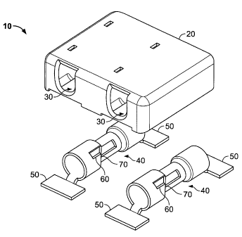
[0018] Referring to FIG. 1, an embodiment of the surface mounted electrical
connector (SMEC) 10 is depicted. A SMEC 10 was formed of a housing 20 with at
CA 02672882 2009-06-16
WO 2008/082533 4 PCT/US2007/025872
least one opening 30 and at least one contact 40. The housing 20 was formed of
Zenite 6330 , a high temperature liquid crystalline polyester by E.I. du Pont
de
Nemours and Company of Wilmington, DE. The heat resistance of the housing
allows it to be attached at the temperatures used to reflow solder the
connector to the
PCB surface.
[0019] The housing may be formed of a high temperature liquid crystalline
polymer (LCP) such as Zenite 6330 or a high temperature nylon such as Stanyl
46
HF or any other known industry acceptable non-conductive high temperature
resin.
[0020] The SMEC 10 allows for the electrical connection of wire leads to the
PCB without having to solder the wire leads to the PCB. The housing 20 was
designed with a low profile and small footprint so that it could be placed
upon a PCB
supporting lighting LEDs without shadowing or blocking the light emissions of
the
LEDs.
[0021] The housing 20 contained at least one opening 30 that was initially
formed
into the housing 20. The housing 20 was formed by injection molding, and the
opening 20 was formed during this step. The opening 30 may be formed after the
initial forming of the housing 20. The housing 20 was designed to allow the
contact
40 to be frictionally fit and retained by the housing 20 by a snap in feature.
[0022] The contact 40 was formed with attachment points 50 to allow the
contact
40 to be joined to a PCB by conventional SMT methods such as soldering. The
contact 40 was formed with a slot 60 and a lance 70 to secure a wire lead upon
insertion into the contact 40.
[0023] Fig. 2 shows a contact 40 with an attachment point 52 with a different
geometry than attachment point 50 of Fig. 1. The shape of the attachment point
52
may vary depending upon the surface area desired to be in contact with the PCB
surface.
[0024] The contact 40 may be attached to a PCB by soldering the attachment
point 50 to the PCB surface. The housing 20 may then be attached to the
contact 40
CA 02672882 2009-06-16
WO 2008/082533 5 PCT/US2007/025872
to form the SMEC 10. Alternatively, the contact 40 may be attached to the
housing
20 to form the SMEC 10, and the SMEC 10 may then be attached to the PCB at the
attachment points 50 by a conventional SMT method such as soldering.
[0025] As an alternative method of attachment, the attachment points 50 may be
further formed to direct the attachment points 50 down 90 degrees so as to
allow the
attachment points to be inserted into through holes formed in a PCB surface.
[0026] Fig. 3 illustrates a more detailed view of an embodiment of the contact
40
with a slot 60 and a lance 70 formed on the bottom side of the contact 40. As
shown
in Fig. 3, the lance 70 is slightly depressed into the contact 40 so as to
engage a wire
lead when inserted into the contact 40. The contact 40 was formed by first
stamping
out a flat pattern blank from a tin plated phosphor bronze sheet. The sheet
was a
phosphor bronze metal of about 320 microns thick with a tin plating of about
3.0 to
about 4.0 microns. It should be noted that the invention is not limited to
this sheet or
plating thickness, and that thinner or thicker sheet and plating may be
selected as
determined by the wire gauge and application. The flat pattern blank was then
partially rolled and worked to form the contact 40 as shown in Figs. 2 and 3
with a
cylindrical portion 42 and an attachment point 52 for attaching the contact 40
to a
substrate such as a PCB.
[0027] The cylindrical portion 42 was formed with an orientation notch 41 to
assist in SMT processing by assisting in mating with the housing 20 to assist
in.
polarization and alignment of the contact 40 attachment points 50, an expanded
cylindrical portion 44 for receiving wire that has insulation thereupon, a
wire lead
portion 45 for receiving wire that has the insulation stripped therefrom. The
contact
40 may be formed without the expanded cylindrical portion 44 to reduce the
size of
the contact 40. The wire lead portion 45 may be formed to accept standard wire
strip
lengths of between about 4 mm and about 7 mm. The wire lead may be a solid
wire, a
fused stranded wire, a stranded wire, a stranded twisted wire, or any other
suitable
wire configuration. As shown in more detail in Fig. 3, a lance 70 was provided
with
a sharp edge 72 to assist in securely engaging an inserted wire lead.
CA 02672882 2011-12-05
67789-606
6
[0028] In an additional embodiment of the invention, the barrel may be used
upon
a PCB without a housing 20. This additional embodiment may reduce
manufacturing and
materials cost in uses where it is less important to shield the barrel from
unwanted
contact.
[0029] In an alternative embodiment of the attachment point as shown in Figs.
4
and 5, the barrel 20 is provided with an alternative attachment point 55. The
attachment
point 55 is shown with a beveled section 82 to assist in solder reflow during
attachment
to a PCB. As further illustrated in Fig. 5, the attachment point 55 is
provided with a
substantially horizontal bottom section 90 and a flat sidewall section 100. A
beveled
section 82 with a thickness of about 50 to about 70 percent of the total
thickness of the
attachment point 55 has provided improved solder reflow properties. The
beveled
section 82, which may be formed by hitting the edge of the attachment point 55
with a
coining operation, the tin plating on the bottom surface is formed on an
angle. The
beveled section 82 allows for the solder to more easily wet the angled tin
face, creating a
fillet of solder that would not otherwise form.
[0030] Figure 6 illustrates an application of an SMEC 720 as a system and
method for attaching wires to a PCB 730. In this illustration, an SMEC 720 is
attached to
a surface of a PCB 730. The SMEC 720 may be attached to the PCB 730 by a
conductive adhesive or solder. The PCB 730 also supports resistors 740 and
LEDs 750.
Wire leads 760 are attached to the PCB 730 via the SMEC 720. In this method,
several
PCBs supporting LEDs may be wired in series to form lighted signs.
[0031] While the invention has been described with reference to a preferred
embodiment, it will be understood by those skilled in the art that various
changes may be
made and equivalents may be substituted for elements thereof without departing
from the
scope of the claims. In addition, many modifications may be made to adapt a
particular
situation or material to the teachings of the invention without departing from
the essential
scope of the claims. Therefore, it is intended that the invention not be
limited to the
particular embodiment disclosed as the best mode contemplated for carrying out
this
invention, but that the invention will include all embodiments falling within
the scope of
the appended claims.