Note: Descriptions are shown in the official language in which they were submitted.
CA 02673043 2009-06-04
WO 2008/071472 PCT/EP2007/060497
1
METHOD AND APPARATUS FOR RECEIVING RADIO FREQUENCY SIGNALS
TECHNICAL FIELD
The present invention generally relates to all wireless receivers, and
particularly relates to direct
frequency down conversion of radio frequency signals in wireless receivers.
BACKGROUND
Information is transmitted in many wireless applications using Radio Frequency
(RF) signals.
RF signals are formed by modulating a baseband signal (information) onto a
carrier signal, the
carrier signal having a frequency greater than the baseband signal frequency.
Upon reception,
an RF signal is finally down converted to a desired baseband frequency before
baseband signal
processing occurs. RF signals may be directly down converted or may be
processed by one or
more intermediate stages before finally being converted to a desired baseband
frequency.
A heterodyne-based receiver down converts a received RF signal via one or more
intermediate
frequency (IF) stages until a desired baseband frequency is obtained. Each IF
stage comprises
a mixer, a filter and/or an amplifier stage. The output of a particular IF
stage has a frequency
corresponding to the difference between a local oscillation signal input to
the mixer and the
frequency of the RF (or IF) input signal.
A homodyne-based receiver eliminates the need for IF stages by directly down
converting a
received RF signal to a desired baseband frequency signal. As such, homodyne-
based
receivers tend to use fewer components than their heterodyne counterparts,
thus resulting in
size and power advantages. A direct-conversion homodyne receiver
conventionally includes a
RF receiver front-end which comprises a Low Noise Amplifier (LNA) for
amplifying a received RF
signal, a mixer for directly down converting the amplified RF signal to a
desired baseband
frequency signal and an impedance matching circuit for matching the output
impedance of the
LNA to the input impedance of the mixer. In full-duplex homodyne receivers, a
surface acoustic
wave filter is conventionally included to filter interference injected from
the transmitter to the
receiver during simultaneous operation.
CA 02673043 2009-06-04
WO 2008/071472 PCT/EP2007/060497
2
Various challenges exist when directly down converting an RF signal to a
desired baseband
frequency signal, particularly when the components used for direct conversion
are integrated
onto the same silicon die using a deep sub-micron CMOS technology. Deep-
submicron CMOS
technologies offer low supply voltages. A low supply voltage limits the linear
operating range of
an LNA. That is, a limited supply voltage limits the output voltage range of
the LNA, thus
causing it to desensitize the gain for weak wanted signals. As such, the LNA
operates in a
nonlinear region when processing high level signal components of an RF signal
unless the gain
of the LNA is adjusted downward. To avoid desensitization of the gain for weak
wanted signals,
good linearity is required for the RF receiver front-end. Normally, passive
mixers provide better
linearity than active mixers. However, passive mixers become difficult to use
because passive
mixers have negative gain and the total gain provided by the LNA and mixer is
not enough,
which results in low RF receiver front-end gain. Low RF receiver front-end
gain requires that
circuits following the mixer must be designed with low noise circuitry.
To compensate for reduced LNA gain, active mixers are conventionally used.
Although active
mixers provide additional gain, they consume more power than their passive
mixer counterparts.
Active mixers also have poor linearity. Further, flicker noise is present in
active mixers.
Although flicker noise does not affect high frequency signals, it does
adversely affect low
frequency signals such as narrowband GSM baseband signals. Flicker noise may
be reduced
by increasing the size of transistors included in an active mixer. However,
larger transistors
consume more power. In addition to power consumption and flicker noise
concerns, active
mixers also have a DC offset, thus causing level shift at the mixer output.
Passive mixers cure
many of the disadvantages associated with active mixers. However, passive
mixers generally
have negative gain. As such, it is increasingly difficult to use traditional
passive mixers and
LNAs using deep sub-micron CMOS technologies due to the low voltage margin
associated with
such technologies and insufficient gain.
CA 02673043 2009-06-04
WO 2008/071472 PCT/EP2007/060497
3
SUMMARY
According to the methods and apparatus taught herein, down conversion of a
received RF
signal to a baseband signal is achieved using a receiver having a passive
mixer, a balun and a
Low-Noise Amplifier (LNA). Gain of the LNA is reduced to minimize nonlinearity
which arises
when signals output by the LNA approach or exceed the linear voltage output
range of the LNA.
The balun couples the LNA output to the passive mixer input. To compensate for
any gain
shortfalls that may result from using the passive mixer or reducing LNA gain,
the balun
comprises a primary winding coupled to the LNA output and a secondary winding
coupled to the
passive mixer input. The secondary winding has more turns than that of the
primary winding,
thus providing voltage gain between the LNA output and the passive mixer
input. The
transformer turn ratio is selected to provide both sufficient voltage gain and
impedance matching
between the LNA output and passive mixer input.
The secondary winding of the balun may be biased with a DC voltage that serves
as a bias
voltage for the passive mixer. Passive mixer nonlinearity may be minimized by
using a
complementary passive mixer having both P-FET and N-FET transistors. Thus, by
properly
selecting the bias voltage and sizing the P-FET and N-FET devices, the
resulting passive mixer
nonlinearity partly cancels or reduces LNA nonlinearity, thus improving the
overall linearity of the
receiver. Since the balun provides voltage gain to compensate for negative
gain in the mixer,
the LNA gain may be maintained relatively low to reduce the LNA nonlinearity.
Low LNA gain
also relaxes LNA design constraints so that low LNA output impedance can be
used. Low LNA
output impedance advantageously improves the frequency tuning range of the
receiver. As
such, proper selection of the balun transformer turn ratio and biasing of the
balun enables the
receiver to down convert received RF signals using a passive mixer without
sacrificing voltage
gain or linearity.
According to one embodiment of the down conversion receiver, the receiver
comprises a
passive mixer, a low-noise amplifier and a balun. The low-noise amplifier is
configured to
generate an amplified single-ended signal responsive to a single-ended
receiver input signal.
The passive mixer is configured to generate a mixer output signal responsive
to a differential
CA 02673043 2009-06-04
WO 2008/071472 PCT/EP2007/060497
4
mixer input signal and a four-phase local oscillator signal. The balun is
configured to transform
the amplified singled-ended signal into the differential mixer input signal,
the balun having a first
winding coupled to an output of the low-noise amplifier and a second winding
coupled to an
input of the passive mixer, the second winding having more turns than the
first winding. The
turn ratio of the second winding to the first winding is configured to provide
gain compensation to
the low-noise amplifier, and in conjunction with the low-noise amplifier and
the passive mixer, to
provide a desired gain to the receiver and linearity over a dynamic range of
the receiver input
signal.
Of course, the present invention is not limited to the above features and
advantages. Those
skilled in the art will recognize additional features and advantages upon
reading the following
detailed description, and upon viewing the accompanying drawings.
BRIEF DESCRIPTION OF THE DRAWINGS
Figure 1 is a block diagram of one embodiment of a wireless communication
device including a
frequency down conversion receiver.
Figure 2 is a block diagram of one embodiment of a frequency down conversion
receiver.
Figure 3 is a block diagram of another embodiment of a frequency down
conversion receiver.
Figure 4 is a timing diagram illustrating a four-phase local oscillation
signal for use with a
passive mixer.
Figure 5 is a graph diagram illustrating varying conducting resistance of one
embodiment of a
passive mixer.
Figure 6 is a graph diagram illustrating varying conducting resistance of
another embodiment of
a passive mixer due to process variation.
Figure 7 is a block diagram of one embodiment of a frequency down conversion
receiver having
a frequency tuning capacitor array.
CA 02673043 2009-06-04
WO 2008/071472 PCT/EP2007/060497
DETAILED DESCRIPTION
Figure 1 illustrates an embodiment of a wireless communication device 10 such
as a mobile
phone, radio, cordless telephone, personal digital assistant, global
positioning system, wireless
Local Area Network (WLAN) adapter such as a wireless network interface
controller, etc. The
5 wireless device 10 receives and transmits information via RF signals. The
device 10 includes a
receiver front-end 12 for down converting a received RF signal r(t) to a
desired baseband
frequency signal BI(t)/BQ(t). Received signals are filtered, e.g., by a
bandpass filter 13, before
being processed by the receiver front-end 12. The device 10 also includes a
demodulator 14,
an analog-to-digital converter 16 and a baseband processor 18 for processing
the baseband
signal B(n), e.g., by performing decoding, symbol estimation, interference
cancellation, bit
synchronization, error correction, etc. Alternatively, the baseband processor
18 also performs
signal demodulation. For heterodyne-based receivers, one or more intermediate-
frequency (IF)
stages (not shown) are included between the receiver front-end 12 and the
demodulator 14 for
down-converting the received signal in successive steps. The wireless device
10 also includes a
transmitter 19 to transmit information via RF signals and a duplexer 21 for
enabling full duplex
(receive and transmit) operation.
The receiver front-end 12 comprises a Low-Noise Amplifier (LNA) 20, a balun
22, a passive
mixer 24 and filters 26 and 28. The receiver front-end 12 provides sufficient
signal gain so that
components downstream from the receiver front-end 12 operate properly in the
presence of
noise. Although the passive mixer 24 mitigates the flicker noise and power
consumption
drawbacks associated with active mixers, it has negative gain. Further, the
LNA 20 operates
with reduced gain to minimize LNA nonlinearity as will be described later. To
compensate for
any gain shortfall, the balun 22 comprises a transformer having an m:n ratio
of primary winding
turns (m) to secondary winding turns (n), the secondary winding being coupled
to inputs of the
passive mixer 24 and the primary winding being coupled to an output of the LNA
20. The
secondary winding has more turns than does the primary winding, i.e., n>m,
thus providing
positive voltage gain at the secondary winding.
CA 02673043 2009-06-04
WO 2008/071472 PCT/EP2007/060497
6
The transformer turn ratio m:n is selected to provide at least enough voltage
gain to compensate
for the reduced gain of the LNA 20 and the use of passive mixer 24. That is,
the balun 22
compensates for the gain shortfall between the total desired receiver front-
end gain and the gain
provided by the LNA 20 and passive mixer 24. The transformer turn ratio is
also selected to
provide sufficient impedance matching between the output impedance of the LNA
20 (which
tends to be low) and the input impedance of the passive mixer 24 (which tends
to be high).
Further, if LNA nonlinearity remains, the passive mixer 24 may be biased by
providing a DC
voltage to the center tap of the secondary winding. Proper selection of the DC
bias voltage
enables the passive mixer 24 to counteract LNA nonlinearity as will be
described in detail later.
Also, by having more turns on the secondary winding, local oscillator clock
signal leakage from
the passive mixer 24 to antenna 30 is reduced since local oscillator clock
signals at the primary
winding have negative voltage gain due to backward transformation. Thus, by
properly selecting
the transformer turn ratio and appropriately biasing the balun 22, impedance
matching is
achieved and the receiver front-end gain requirement satisfied while
minimizing the effects of
LNA nonlinearity.
In more detail, the received RF signal r(t) is amplified by the LNA 20. The
LNA 20 has a gain a
that is less than the desired total receiver front-end gain. The LNA gain is
selected to reduce
LNA nonlinearity, particularly when the LNA 20 amplifies high level signal
components of the RF
signal r(t). Maintaining the LNA gain sufficiently low when the LNA 20
amplifies high level signal
components reduces LNA nonlinearity caused by a limited output voltage range
of the LNA 20.
Lower LNA gain allows lower LNA output impedance. The frequency tuning range
of the
receiver front end 12 is beneficially increased when LNA output impedance is
low as will be
described in detail later.
The balun 22, which inductively couples the output of the LNA 20 to the inputs
of the passive
mixer 24, transforms the amplified signal ar(t) into a differential signal
having total voltage gain
of P. The total voltage gain P is the sum of the LNA voltage gain a and the
balun voltage gain k,
where k=n/m when the balun 22 is lossless. The passive mixer 24 directly down
coverts the
CA 02673043 2009-06-04
WO 2008/071472 PCT/EP2007/060497
7
mixer input signal Pr(t) to In-phase and Quadrature (I/Q) signals, BI (t) and
BQ (t) . The
demodulator 14 recovers the baseband information B(t) by demodulating the I/Q
signals.
Returning to the balun 22, its voltage gain k is a function of the ratio [ n]
where n is the number
rn
of secondary transformer winding turns and m is the number of primary winding
turns. Thus, to
increase the balun voltage gain, the ratio of secondary to primary winding
turns is increased.
The transformer turn ratio is also selected such that a desired impedance
matching between the
output of the LNA 20 and the input of the passive mixer 24 is realized. If the
balun 22 is
lossless, the impedance seen by the LNA 20 looking into the primary coil of
the balun 22 (Zprm) is
related to the impedance seen by the passive mixer 24 looking into the
secondary coil of the
balun 22 (ZSeC) as given by:
z
= [ n ]
sec
Zsec
(1)
Thus, the output impedance of the LNA 20 (ZLNA) may be sufficiently matched to
the input
impedance of the passive mixer 24 (ZMIx) by selecting a transformer turn ratio
that satisfies
[ 15 n 2=ZLNA
n] ZMIX
(2)
Accordingly, the greater the impedance ratio of ZMIx to ZLNA, the greater the
ratio of secondary
winding turns to primary winding turns. Since ZLNA ZMIx for most integrated
circuit
implementations, it is feasible to have n>m, thus positive voltage gain is
achieved. The
transformer turn ratio may be set once, e.g., during circuit design or may be
programmable.
Regardless, the selection of the transformer turn ratio enables the receiver
front-end 12 to utilize
a passive mixer 24 and a reduced gain LNA 20 without sacrificing gain or
linearity.
Figure 2 illustrates an embodiment of the receiver front-end 12. The amplified
LNA output signal
ar(t) excites one end of a primary transformer winding 32 while the opposite
end is connected to
CA 02673043 2009-06-04
WO 2008/071472 PCT/EP2007/060497
8
a DC supply voltage Vdd. The balun 22 transforms the amplified LNA output
signal to a
differential signal via a secondary winding 34 with voltage gain k of the
balun 22 being a function
of the ratio1 11>1. The number of primary and secondary winding turns is
selected to provide
rn
sufficient impedance matching and gain compensation as previously described. A
tuning
network 36 adjusts the frequency range of the receiver front end 12. The
differential signal
output by the balun 22 is input to the passive mixer 24.
The passive mixer 24 includes an in-phase mixer 38 (I-channel mixer) and a
quadrature mixer
40 (Q-channel mixer). The differential balun output signals +pr(t)/2 and -
pr(t)/2 are provided to
the I/Q-channel mixer 38 and 40, respectively. The I/Q-channel mixer 38 and 40
down-converts
the mixer input signals by multiplying the signals with local oscillation
signals. The local
oscillation signals may be multi-phase as described in detail later.
Regardless, the filters 26 and
28, e.g., low pass or bandpass filters, remove high frequency products of the
mixing process to
yield I/Q signals having a desired baseband frequency. The desired baseband
frequency is a
function of the local oscillation frequency and RF input signal frequency as
is well known in the
art.
According to this embodiment and equations (1) and (2), the impedance at the
primary winding
32 of the balun 22 is a function of the impedance at the secondary winding 34
and the ratio m:n
of primary winding turns (m) to secondary winding turns (n). The impedance at
the secondary
winding 34 is related to the input impedance of the passive mixer 24. The
input impedance of
the passive mixer 24 is a function of the mixer's output impedance and the
input impedance of
the filters 26 and 28. When configured for homodyne-based direct conversion,
the filters 26 and
28 are configured as baseband low pass filters. When configured for heterodyne-
based
frequency down-conversion, the filters 26 and 28 are configured as
intermediate frequency (IF)
bandpass filters.
The amount of signal attenuation provided by the filters 26 and 28 is
frequency dependent.
Thus, the input impedance of the filters 26 and 28 depends on the frequency of
the signals to be
filtered. The filters 26 and 28 have an input impedance that is lower for stop
band frequencies
CA 02673043 2009-06-04
WO 2008/071472 PCT/EP2007/060497
9
than it is for pass band frequencies. For example, when configured for
homodyne-based direct
conversion, the filters 26 and 28 may comprise a first order RC low pass
filter having a resistor
and capacitor where one node of the resistor is connected to one node of the
capacitor to form
an output node while the other node of the resistor forms the input node of
the low pass filter.
The capacitor is connected to ground and provides high input impedance at
lower frequencies
for in-band frequency components and low impedance at higher frequencies for
out-band
frequency components.
The impedance of the filters 26 and 28 is reflected at the output of LNA 20
through the balun 22.
Thus, lower impedance for out-of-band frequency components results in low LNA
gain.
Accordingly, the LNA 20 will have different gains for desired in-band and
undesired out-of-band
RF input signals. Particularly, the LNA 20 has a higher gain for desired in-
band signals than for
undesired out-of-band signals, thus improving the frequency selectivity of the
receiver front end
12.
Power may leak from the transmit side of the device to the receive side when
the device 10
operates in full duplex mode, i.e., when the device 10 transmits and receives
signals
simultaneously, e.g., in WCDMA applications. During full duplex operation,
power leakage from
the transmitter 19 to the receiver front-end 12 is often the largest source of
interference power
present at the input to LNA 20. The configuration of the receiver front end 12
attenuates signals
transmitted by the transmitter 19 in the filters at the mixer 24 base-band
side for homodyne
direct down-conversion (or intermediate frequency side for heterodyne down
conversion), and
through the passive mixer 24 impedance transformation, the transmitted signals
are also
attenuated at the input of the mixer 24. Because the balun 22 inductively
couples the LNA 20 to
the passive mixer 24, signals transmitted by the transmitter 19 are also
attenuated at the LNA
20. Attenuating signals transmitted by the device 10 at the LNA 20 reduces
transmission power
leakage caused by the transmitter 19. Also, maintaining low LNA output
impedance improves
receiver front end linearity while reducing desensitization caused by power
leakage from the
transmitter 19.
CA 02673043 2009-06-04
WO 2008/071472 PCT/EP2007/060497
According to this embodiment, the secondary winding 32 of the balun 22 is
biased at a selected
DC voltage Vb;as. The bias voltage is injected into the secondary winding 32
via a winding tap,
preferably a center tap. The secondary winding 34 provides the bias voltage to
the drain/source
of transistors (not shown) forming the passive mixer 24. When biased at a
proper DC voltage,
5 the transistors contribute to the nonlinearity of the passive mixer 24 due
to non-ideal switching
property of the transistors, e.g., FET or MOSFET devices. The passive mixer 24
may be a
complementary passive mixer which minimizes nonlinearity when its transistors
are properly
balanced and an appropriate secondary winding bias voltage is selected as will
be described in
detail later. Even though LNA gain may be reduced to mitigate nonlinearity,
some LNA
10 nonlinearity may remain, particularly when the LNA 20 amplifies high level
signal components of
a received RF signal. The nonlinearity introduced by the passive mixer 24 may
be designed to
partly cancel LNA nonlinearity by appropriately selecting the secondary
winding bias voltage and
properly sizing the devices forming the complementary passive mixer 24.
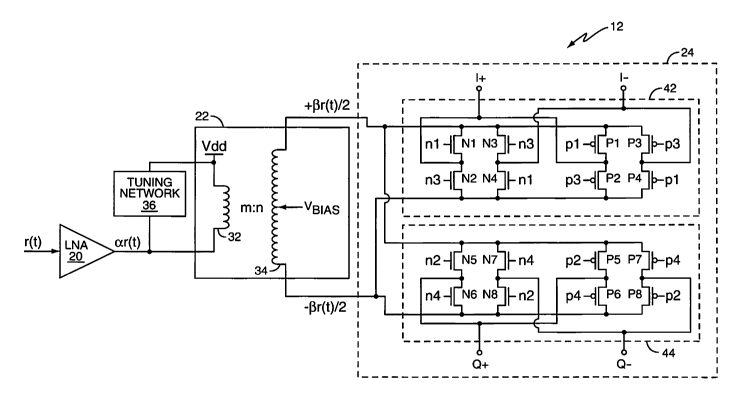
Figure 3 illustrates another embodiment of the receiver front-end 12 where I-
channel mixer 42
and Q-channel mixer 44 in the passive mixer 24 are complimentary mixers. Each
complimentary mixer comprises four N-FETs (N1-N4 in I-channel mixer 42 and N5-
N8 in Q-
channel mixer 44) and four P-FETs (P1-P4 in I-channel mixer 42 and P5-P8 in Q-
channel mixer
44). Nonlinearity introduced by the complimentary passive mixer 24 counteracts
LNA
nonlinearity when the transistors N1-N8 and P1-P8 are properly sized and
biased.
In more detail, the I-channel mixer 42 comprises two sets of cascaded N-FET
transistors (N1-
N4) clocked by positive local oscillation signals (n1 and n3) and two sets of
cascaded P-FET
transistors (P1-P4) clocked by negative local oscillation signals (p1 and p3).
Similarly, the Q-
channel mixer 44 also comprises two sets of cascaded N-FET transistors (N5-N8)
clocked by
positive local oscillation signals (n2 and n4) and two sets of cascaded P-FET
transistors (P5-P8)
clocked by negative local oscillation signals (p2 and p4).
The cascaded sets of N-FET and P-FET transistors in each I/Q-channel mixer 42
and 44 share
two common nodes, one common node being coupled to a first end of the
secondary winding 34
and the other common node being coupled to the opposite end. For example, the
end of the
CA 02673043 2009-06-04
WO 2008/071472 PCT/EP2007/060497
11
secondary winding 34 that outputs the signal +pr(t)/2 is coupled to the common
node shared by
transistors N1, N3, P1 and P3 in the I-channel mixer 42 and transistors N5,
N7, P5 and P7 in the
Q-channel mixer 44. Likewise, the end of the secondary winding 34 that outputs
the signal -
Pr(t)/2 is coupled to the common node shared by transistors N2, N4, P2 and P4
in the I-channel
mixer 42 and transistors N6, N8, P6 and P8 in the Q-channel mixer 44.
During operation, the transistors in the I/Q-channel mixers 42 and 44 operate
as switches, their
operation being controlled by local oscillation clock signals having four
phases. Two clock
signals (n1 and n3) and their complements (p1 and p3) have first and third
phases that control
the transistor gates of the I-channel mixer 42. Two other clock signals (n2
and n4) and their
complement signals (p2 and p4) have second and fourth phases that control the
transistor gates
of the Q-channel mixer 44. Figure 4 illustrates the duty cycle and phases of
the different clock
signals.
The phases of the clock signals are staggered such that only one of the I/Q-
channel mixers 42
or 44 is active at any point in time, where a positive clock pulse activates N-
FET transistor gates
and a negative clock pulse activates P-FET transistor gates. For example, when
clock signal n1
and its compliment p1 are active (positive and negative, respectively) during
the first phase,
transistors N1, P1, N4, and P4 are on in the I-channel mixer 42 while all
other transistors are off.
As such, the I-channel mixer 42 outputs a differential In-phase signal
component at the output
nodes I+ and L. When clock signal n2 and its compliment p2 are active during
the second phase,
transistors N5, P5, N8 and P8 are active in the Q-channel mixer 44 while all
other transistors are
off. Accordingly, the Q-channel mixer 44 outputs a differential Quadrature
signal component at
the output nodes Q+ and Q. The remaining clock signals and their compliments
are activated in
turn, thus yielding differential I/Q signals.
The differential I/Q signals are then low-pass filtered to remove high
frequency harmonics as
previously described. The frequencies of the four-phase clock signal and the
RF input signal
determine the baseband signal frequency. While a four-phase clocking scheme is
preferred,
any phase clocking scheme may be used such as two-phase local oscillation.
Regardless, the
CA 02673043 2009-06-04
WO 2008/071472 PCT/EP2007/060497
12
conducting resistance of the complimentary passive mixer 24 is a function of
the secondary
winding bias voltage and the mixer input signal. Thus, as the mixer input
signal fluctuates, so
too does the conducting resistance of the complimentary passive mixer 24. As a
result, the
complimentary passive mixer 24 attenuates I/Q output signals more when the
mixer's
conducting resistance is high and less when its conducting resistance is low.
Preferably, the nonlinearity of the conducting resistance of the complimentary
passive mixer 24
partly cancels LNA nonlinearity, thus improving the overall linearity of the
receiver front-end 12.
Nonlinearity occurs in the LNA 20 when the received RF signal r(t) approaches
high signal
levels, such as reaching a compression point of the LNA 20. When this occurs,
the limited
supply voltage available to the LNA 20 causes the LNA output to be clipped,
thus reducing LNA
gain for high input signal levels. The voltage output range of the LNA 20 is
limited by the
available supply voltage. This is particularly a concern when receiver
components are
fabricated using deep-sub micron CMOS technologies where very limited supply
voltage ranges
are available. To the contrary, LNA gain reduction is not a concern when the
received RF signal
is at a low level because the LNA 20 has sufficient output voltage margin.
Preferably, the bias
voltage applied to the secondary winding 34 causes the conducting resistance
of the
complimentary passive mixer 24 to vary in a manner that substantially cancels
LNA nonlinear
behavior at high signal levels. Nonlinearity cancellation may be valid only
for certain ranges of
signal levels beyond which linearity degrades sharply.
By way of example, the secondary winding 34 is biased at approximately one
half the supply
voltage (Vdd/2). Figure 5 graphically illustrates how the conducting
resistance of the
complimentary mixer 24 varies in response to the mixer input signal when the
secondary
winding 34 is biased at Vdd/2. Also illustrated in Figure 5 are a weak RF
signal (with small signal
level) and a strong RF signal (with high signal level). The conducting
resistance of the
complimentary mixer 24 is low when the RF signal level is high, thus, the high
level signal is
subjected to less attenuation in the complimentary mixer 24. Recall, when the
LNA output is
high, nonlinearity may be present in the LNA 20, thus resulting in reduced LNA
gain. The
CA 02673043 2009-06-04
WO 2008/071472 PCT/EP2007/060497
13
reduced conducting resistance lessens signal loss by the complimentary mixer
24, thus
minimizing the effects of reduced LNA gain.
To the contrary, when the LNA output is low, the balun 22 output drifts toward
the secondary
winding bias voltage (Vdd/2 in this example). As such, voltages applied to the
common nodes
of the complimentary mixer 24 are both at approximately Vdd/2. When this
occurs, the
conducting resistance of the complimentary mixer 24 increases since the
transistors that are
activated have higher channel resistance, and thus conduct weakly. The mixer
input signal is
thus subjected to increased attenuation. As a result, low-level LNA output
signals are
attenuated more by the complimentary mixer 24 than are high-level LNA output
signals.
In the previous example, the selection of Vdd/2 for the secondary winding bias
voltage
presumes sufficient transistor matching in the complimentary passive mixer 24.
However, if the
current driving capabilities of the P-FETs and N-FETs forming the
complementary passive mixer
24 are not sufficiently balanced, e.g., due to process variation, the bias
voltage applied to the
secondary winding 34 may be altered to bring the complimentary mixer 24 back
into balance,
thus optimizing receiver front end linearity. For example, if the P-FETs have
greater current
drive capability than the N-FETs, the bias voltage applied to the secondary
winding 34 is
decreased below one half the supply voltage. By doing so, the channel
resistance of the P-FET
transistors is balanced at a new point Vpo as shown in Figure 6. Likewise, if
the N-FETs have
greater current drive capability, the bias voltage applied to the secondary
winding 34 is
increased above one half the supply voltage also as shown in Figure 6. By
doing so, the
channel resistance of the N-FET transistors is balanced at a new point Vno. As
such, the bias
voltage may be programmable to accommodate for transistor mismatches, e.g.,
due to process
variations, temperature changes, etc.
Figure 7 illustrates an embodiment of the receiver front end 12 where the
frequency tuning
network 36 comprises a tuning capacitor array coupled to the primary winding
32 of the balun
22. The tuning capacitor array 36 comprises a plurality of control transistors
T1-TN coupled in
parallel. The source and drain of each control transistor has a tuning
capacitor coupled thereto,
e.g., C1 and C2 are coupled to T1, C3 and C4 are coupled to T2, etc. The
control transistors
CA 02673043 2009-06-04
WO 2008/071472 PCT/EP2007/060497
14
T1-TN determine which capacitors are switched into the tuning network, thus
determining the
frequency tuning range of the receiver front-end 12.
Since the balun 22 provides positive voltage gain as previously described, the
gain of the LNA
20 may be reduced to avoid nonlinearity. When LNA gain is reduced, the LNA
output
impedance becomes very low. Maintaining very low LNA output impedance enables
the
frequency tuning range of the receiver front-end12 to be advantageously
increased. To
accommodate a desired increase in receiver frequency tuning range, the tuning
capacitor array
36 adjusts its tuning capacitance accordingly. Thus, the tuning capacitor
array 36 enables the
LNA 20 to accommodate greater frequency tuning ranges.
The frequency tuning range r of the receiver front-end 12 is given by:
/ max ~tmax + cp
J" - -
f.n Ctniin + Cp
(3)
where fmax and fmin are the maximum and minimum operating frequencies of the
receiver front-
end 12, respectively, Ctmax and Ctmin are the maximum and minimum tuning
capacitances of the
tuning capacitor array 36, respectively, and Cp is the parasitic capacitance
at the output node of
the LNA 20. From equation (3), a decrease in the minimum tuning capacitance
Ctmin results in a
corresponding increase in the frequency tuning range of the receiver front-end
12.
In more detail, the LNA 20 comprises first and second transistors TC1 and TC2.
Transistors
TC1 and TC2 form a cascaded LNA amplification stage for amplifying the
received RF signal
r(t). A bias resistor RB provides DC bias to the gate of transistor TC2 while
the supply voltage
Vdd biases the gate of transistor TC1. The received RF signal is coupled to
the gate of TC2 via
inductance Lg, where Cpa is the input parasitic capacitance and Ls is the
source degeneration
inductance. The cascaded amplifier stage formed by transistors TC1 and TC2
yields an
amplified version ar(t) of the RF input signal. The amplified signal is
provided to one end of the
primary winding 32 while the opposite end is biased at the supply voltage Vdd.
The tuning
CA 02673043 2009-06-04
WO 2008/071472 PCT/EP2007/060497
capacitor array 36 is coupled between the inputs to the primary winding 32 and
determines the
frequency tuning range of the receiver front-end 12.
A control word (TUNE<1:n>) input to the gates of the control transistors
determines which
transistors are switched on and which ones are not. The tuning capacitors
coupled in series
5 with each activated control transistor determine the overall tuning
capacitance of the receiver
front end 12 as given by equation (3). When one of the control transistors T1-
TN is switched off,
the corresponding parasitic diode pair D1/D2 through D2N-1/D2N associated with
the source
and drain of the deactivated control transistor contributes to the tuning
capacitance. For
example, if control transistor T1 is switched off, parasitic diodes D1 and D2
contribute junction
10 capacitance to the ground node. As such, the tuning capacitance Ct is a
function of the
capacitance of capacitor C1 and the junction capacitance of diode D1. Diode D1
is reverse
biased at a high potential to reduce its junction capacitance.
In general, an inverter 46-50 associated with each deactivated control
transistor creates a high
potential responsive to the control word and feeds it through corresponding
resistor pairs RO/R1
15 and R2N-1/R2N to respective cathodes of the diode pair (D1/D2, D3/D4, D2N-
1/D2N)
associated with each deactivated control transistor. For example, if
transistor T1 is deactivated,
the control word causes inverter 46 to drive resistors RO and R1 with a high
potential which is
applied to the cathodes of diodes D1 and D2. The bulk of the transistor T1-TN
is biased to
ground, so the parasitic diodes associated with the deactivated transistor are
reversed biased,
thus reducing the parasitic capacitance of the diodes. When one or more of the
control
transistors are switched on, the source and drain of each activated control
transistor are
preferably biased to ground to reduce the on-resistance associated with the
activated
transistors, thus enabling the frequency tuning capacitor array 36 to have
high Q. Of course,
various other tuning capacitor embodiments may be used to adjust the frequency
tuning range
of the receiver front-end 12 in response to changes in LNA output impedance,
and thus, are
within the scope of the present invention.
With the above range of variations and applications in mind, it should be
understood that the
present invention is not limited by the foregoing description, nor is it
limited by the
CA 02673043 2009-06-04
WO 2008/071472 PCT/EP2007/060497
16
accompanying drawings. Instead, the present invention is limited only by the
following claims,
and their legal equivalents.