Note: Descriptions are shown in the official language in which they were submitted.
CA 02673330 2009-06-18
WO 2008/088669 PCT/US2008/000006
SEMICONDUCTOR NANOSTRUCTURES, SEMICONDUCTOR DEVICES, AND
METHODS OF MAKING SAME
FIELD OF THE INVENTION
[0001] The present invention generally relates to semiconductor nanostructures
with a
core-shell configuration that can be used for forming nano-sized semiconductor
devices. More specifically, the present invention relates to field effect
transistors
(FETs) formed by such semiconductor nanostructures, as well as to methods for
forming the FETs.
BACKGROUND OF THE INVENTION
[0002] Miniaturization of semiconductor devices, such as field effect
transistors
(FETs), has been the main driving force behind the incredible progress in the
area of
computation over the last half decade. Use of smaller FETs advantageously
results in
a higher packing density, as well as improved device performance. To further
sustain
this trend, novel nanostructures are explored as possible successors of the
current
state-of-art silicon devices. One type of nanostructure considered as
particularly
promising for forming nano-sized FETs is a semiconductor nanowire grown by
homo-
epitaxy (such as a germanium or silicon nanowire).
[0003] However, building devices from semiconductor nanowires requires
reinventing the conventional complementary metal-oxide-semiconductor (CMOS)
process flow and redesigning desired doping profiles and implementation
details, so
that such semiconductor nanowires may become the central portions of new high
performance nano-sized FETs.
[0004] The conventional nano-sized FET contains a rather simple (i.e., non-
ideal)
semiconductor nanowire structure. Specifically, a top or bottom gate is used
to
control the electrostatics inside a channel region of the FET, which is
located in the
uniformly doped or undoped semiconductor nanowire, and source/drain metal
contacts for the FET are attached to the two ends of the semiconductor
nanowire. In
1
CA 02673330 2009-06-18
WO 2008/088669 PCT/US2008/000006
such a FET configuration, the gate not only controls the electrostatics inside
the
channel region, but also impacts the injection properties at the
metal/nanowire
interface. This unavoidably results in a transmission probability that is
substantially
smaller than unity through this interface when an undoped nanowire is used, or
in a
very substantial shift of the threshold voltage when a uniformly doped
nanowire is
used for improving the contact quality.
[0005] The desired approach would involve a more complicated doping profile
with a
highly doped region located close to the metal contacts and a lowly doped or
undoped
region located close to the gate, but away from the contacts.
[0006] Currently, there are two standard approaches for realizing such a
complicated
doping profile in a nanowire - both suffering from substantial drawbacks. One
approach is to grow the semiconductor nanowires in situ with a desired doping
profile
along the length of the nanowire. This approach, however, is incompatible with
the
requirement for precisely aligning the FET components, such as the gate and
the
source/drain metal contacts, at a later stage to this doping profile.
Consequently, the
parasitic capacitance contributions cannot be reduced as desirable, which
ultimately
limits improvement in the device performance. The second approach is to
implant
dopants into an existing semiconductor nanowire, using conventional dopant
implantation techniques. It is highly desirable to use nanowires in a three-
dimensional integrated approach, but the implanted dopant cannot form a
uniform
doping profile in various depths of the nanowire relative to the implantation
direction.
In addition, it is highly questionable whether it is possible to use an ion
implantation
approach for any nanostructure, since the ions would have to be "stopped" very
precisely within the nanostructure.
[0007] There is therefore a continuing need for improved nanostructures with
desired
doping profiles that are suitable for forming FET devices.
SUMMARY OF THE INVENTION
[0008] The present invention provides a three-dimensional nanostructure with a
doping profile characterized by uniform dopant concentrations along a
longitudinal
2
CA 02673330 2009-06-18
WO 2008/088669 PCT/US2008/000006
axis of the nanostructure and differential dopant concentrations in a radial
direction
thereof. Such a three-dimensional nanostructure is formed by using a
combination of
lithographical and deposition techniques, without the need for dopant
implantation.
[0009] In one aspect, the present invention relates to semiconductor structure
comprising multiple sections arranged along a longitudinal axis of the
semiconductor
structure, wherein a semiconductor core having a first dopant concentration
extends
along the longitudinal axis through the multiple sections of the semiconductor
structure, and wherein a semiconductor shell having a second, higher dopant
concentration encircles a portion of the semiconductor core at one or more,
but not all,
sections of the semiconductor structure.
[0010] Preferably, the semiconductor structure of the present invention has a
middle
section and two terminal sections located at opposite ends of the middle
section. The
semiconductor core extends through the middle section and two terminal
sections of
the semiconductor structure, and the semiconductor shell encircles a portion
of the
semiconductor core at the two terminal sections, but not at the middle
section, of the
semiconductor structure. More preferably, the semiconductor structure of the
present
invention is preferably a nanostructure with a cross-sectional dimension of
not more
than about 100 nm.
[0011] The semiconductor core and the semiconductor shell comprise any
suitable
semiconductor material. It is noted that in the present invention the
semiconductor
core and the semiconductor shell comprise the same semiconductor material.
[0012] In a specific embodiment of the present invention, the semiconductor
core is
undoped, while the semiconductor shell is doped with ari n-type or a p-type
dopant.
Alternatively, both the semiconductor core and the semiconductor shell can be
doped
with an n-type dopant, provided that the first dopant concentration ranges
from about
10" to about 10" atoms/cm3, and the second, higher dopant concentration ranges
from about 1017 to about 1021 atoms/cm3. Further, both the semiconductor core
and
the semiconductor shell can be doped with a p-type dopant, provided that the
first
dopant concentration ranges from about 101 1 to about 1017 atoms/cm3, and the
second,
higher dopant concentration ranges from about 1017 to about 1021 atoms/cm3.
3
CA 02673330 2009-06-18
WO 2008/088669 PCT/US2008/000006
[0013] In another aspect, the present invention relates to a method
comprising:
forming a semiconductor structure having a longitudinal axis, wherein
a semiconductor core having a first dopant concentration extends along the
longitudinal axis, and wherein a semiconductor shell having a second,
higher dopant concentration also extends along the longitudinal axis and
encircles the semiconductor core; and
selectively removing a portion of the semiconductor shell from at least
one section of the semiconductor structure, so that a remaining portion of
the semiconductor shell encircles a portion of the semiconductor core at
other sections, but not the at least one section, of the semiconductor
structure.
[0014] Preferably, the portion of the semiconductor shell is selectively
removed by:
forming a patterned mask layer to selectively cover the other sections,
but not said at least one section, of the semiconductor structure, wherein
the portion of the semiconductor shell to be selectively removed is
exposed at the at least one section of the semiconductor structure;
oxidizing the exposed portion of the semiconductor shell to form a
semiconductor oxide at the at least one section of the semiconductor
structure;
selectively etching the semiconductor oxide; and
optionally, repeating the oxidizing and selective etching steps until the
exposed portion of the semiconductor shell is completely removed to
expose an underlying portion of the semiconductor core at the at least one
section of the semiconductor structure.
[0015] In a specific embodiment of the present invention, the portion of the
semiconductor shell is removed from a middle section of the semiconductor
structure,
so that the remaining portion of the semiconductor shell encircles a portion
of the
semiconductor core at two terminal sections at opposite ends of the middle
section,
but not at the middle section of the semiconductor structure.
4
CA 02673330 2009-06-18
WO 2008/088669 PCT/US2008/000006
[0016] In a further aspect, the present invention relates to a semiconductor
device
comprising:
a semiconductor structure comprising a middle section and two
terminal sections located at opposite ends of the middle section along a
longitudinal axis of said semiconductor structure, wherein a semiconductor
core having a first dopant concentration extends along the longitudinal axis
through the middle section and the two terminal sections of the
semiconductor structure, and wherein a semiconductor shell having a
second, higher dopant concentration encircles a portion of the
semiconductor core at the two terminal sections, but not the middle section,
of the semiconductor structure; and
a field effect transistor (FET) comprising a source located at one of the
two terminal sections of the semiconductor structure, a channel located at
the middle section of the semiconductor structure, a drain located at the
other of the two terminal sections of the semiconductor structure, and a
gate structure over a portion of the semiconductor core at the middle
section of the semiconductor structure.
100171 The gate structure as mentioned hereinabove may comprise a gate
dielectric
layer and a gate conductor layer. The semiconductor device may further
comprise
metal contacts located over the source and drain of the FET, or metal silicide
layers
between the metal contacts and the source and drain of the FET.
[0018] In a still further aspect of the present invention, the present
invention relates to
a method for forming a semiconductor device comprising:
forming a semiconductor structure having a longitudinal axis, wherein
a semiconductor core having a first dopant concentration extends along the
longitudinal axis, and wherein a semiconductor shell having a second,
higher dopant concentration also extends along the longitudinal axis and
encircles the semiconductor core;
selectively removing a portion of the semiconductor shell from a
middle section of the semiconductor structure, so that a remaining portion
of the semiconductor shell encircles a portion of the semiconductor core at
CA 02673330 2009-06-18
WO 2008/088669 PCT/US2008/000006
two terminal sections at opposite ends of the middle section, but not at the
middle section of the semiconductor structure; and
forming a field effect transistor (FET) from the semiconductor
structure, wherein the FET comprises a source located at one of the two
terminal sections of the semiconductor structure, a channel located at the
middle section of the semiconductor structure, a drain located at the other
of the two terminal sections of the semiconductor structure, and a gate
structure over a portion of the semiconductor core at the middle section of
the semiconductor structure.
[0019] Preferably, the FET as mentioned hereinabove is formed by:
forming a gate dielectric layer over the portion of the semiconductor
core at the middle section of the semiconductor structure; and
forming a gate conductor layer over the gate dielectric layer at the
middle section of the semiconductor structure, wherein the portion of the
semiconductor core at the middle section of the semiconductor structure,
which is covered by the gate dielectric layer and gate conductor layer,
forms the channel of the FET, wherein one of the two terminal sections
located at one end of the middle section of the semiconductor structure
forms the source of the FET, and wherein the other of the two terminal
sections located at the other, opposite end of the middle section of the
semiconductor structure forms the drain of the FET.
BRIEF DESCRIPTION OF THE DRAWINGS
[0020] FIG. 1 shows a side view of a semiconductor nanostructure containing a
differentially doped semiconductor core and shell, while a portion of the
semiconductor shell is removed from a middle section of the semiconductor
nanostructure to expose the underlying semiconductor core, according to one
embodiment of the present invention.
[0021] FIG. 2 shows a side view of a field effect transistor (FET) formed
using the
semiconductor nanostructure of FIG. 1, while the FET contains a channel region
6
CA 02673330 2009-06-18
WO 2008/088669 PCT/US2008/000006
located at the middle section of the semiconductor nanostructure and
source/drain
regions located at two terminal sections of the semiconductor nanostructure,
according to one embodiment of the present invention.
[0022] FIGS. 3-4 illustrate exemplary processing steps for forming the
semiconductor
nanostructure of FIG. 1, according to one embodiment of the present invention.
[0023] FIGS. 5-9 illustrate exemplary processing steps for forming the FET of
FIG. 2
by using the semiconductor nanostructure of FIG. 1, according to one
embodiment of
the present invention.
[0024] DETAILED DESCRIPTION OF THE INVENTION, AND PREFERRED
EMBODIMENTS THEREOF
[0025] In the following description, numerous specific details are set forth,
such as
particular structures, components, materials, dimensions, processing steps and
techniques, in order to provide a thorough understanding of the present
invention.
However, it will be appreciated by one of ordinary skill in the art that the
invention
may be practiced without these specific details. In other instances, well-
known
structures or processing steps have not been described in detail in order to
avoid
obscuring the invention.
[0026] It will be understood that when an element as a layer, region or
substrate is
referred to as being "on" another element, it can be directly on the other
element or
intervening elements may also be present. In contrast, when an element is
referred to
as being "directly on" another element, there are no intervening elements
present. It
will also be understood that when an element is referred to as being
"connected" or
"coupled" to another element, it can be directly connected or coupled to the
other
element or intervening elements may be present. In contrast, when an element
is
referred to as being "directly connected" or "directly coupled" to another
element,
there are no intervening elements present.
[0027] While the invention has been described herein with reference to
specific
embodiments, features and aspects, it will be recognized that the invention is
not thus
7
CA 02673330 2009-06-18
WO 2008/088669 PCT/US2008/000006
limited, but rather extends in utility to other modifications, variations,
applications,
and embodiments, and accordingly all such other modifications, variations,
applications, and embodiments are to be regarded as being within the spirit
and scope
of the invention.
[0028] The present invention provides an improved semiconductor structure,
which is
preferably an improved semiconductor nanostructure having a cross-sectional
dimension of not more than about 100 nm.
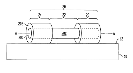
[0029] FIG. 1 shows an exemplary semiconductor structure 20, according to one
embodiment of the present invention. Specifically, the semiconductor structure
20 is
located over an upper surface 12 of a substrate 10 and has a core-shell
configuration
including a semiconductor core 20C and a semiconductor she1120S.
[0030] The substrate 10 may comprise any semiconductor or insulating
materials.
Preferably, the substrate 10 comprises a semiconductor material selected from
the
group consisting of: Si, SiC, SiGe, SiGeC, Ge alloys, GaAs, InAs, InP, as well
as
other III-V or II-VI compound semiconductors. The substrate 10 may also
comprise
an organic semiconductor or a layered semiconductor such as Si/SiGe, a silicon-
on-
insulator (SOI) or a SiGe-on-insulator (SGOI). In some embodiments of the
present
invention, it is preferred that the substrate 10 be composed of a Si-
containing
semiconductor material, i.e., a semiconductor material that includes silicon.
The
substrate 10 may be doped or undoped, or it may contain both doped and undoped
device regions therein. Further, the substrate 10 may comprise one or more
isolation
regions between adjacent device regions.
[0031] The semiconductor structure 20 is preferably a nanostructure having a
cross-
sectional dimension of not more than about 100 nm. The semiconductor core 20C
and the semiconductor she1120S of the semiconductor nanostructure 20 can be
formed
of any suitable semiconductor material, including, but not limited to: Si,
SiC, SiGe,
SiGeC, Ge alloys, GaAs, InAs, InP, as well as other III-V or II-VI compound
semiconductors.
8
CA 02673330 2009-06-18
WO 2008/088669 PCT/US2008/000006
[0032] Preferably, the semiconductor core 20C and the semiconductor shell 20S
comprise the same semiconductor material, but with different doping levels.
For
example, both 20C and 20S may comprise Si or SiGe, but the semiconductor 20C
either is undoped or is doped with a dopant species (either an n-type or p-
type dopant)
at a first, relatively low doping concentration, while the semiconductor 20S
is doped
with the same (comment: if the doping profile n/p/n or p/n/p is chosen, the
device may
still prove useful but dopant fluctuation for ultimately scaled devices may
prove
harmful in the channel region) dopant species (either an n-type or p-type
dopant) at a
second, relatively high doping concentration.
[0033] In a preferred embodiment of the present invention, both the
semiconductor
core 20C and the semiconductor she1120S are doped with an n-type dopant, such
as
phosphorus, arsenic, and antimony. More preferably, the semiconductor core 20C
has
a first, relatively low dopant concentration ranging from about 10" to about
1017
atoms/cm3, and the semiconductor she1120S has a second, relatively high dopant
concentration ranging from about 1017 to about 1021 atoms/cm3.
[0034] In an alternative embodiment of the present invention, both the
semiconductor
core 20C and the semiconductor she1120S are doped with a p-type dopant, such
as
aluminum, gallium, and indium. Preferably, the semiconductor core 20C has a
first,
relatively low dopant concentration ranging from about 1011 to about 1017
atoms/cm3,
and the semiconductor she1120S has a second, relatively high dopant
concentration
ranging from about 1017 to about 1021 atoms/cm3.
[0035] The semiconductor nanostructure 20 may comprise multiple sections
arranged
along a longitudinal axis A-A of the semiconductor structure 20. Preferably,
but not
necessarily, the semiconductor nanostructure 20 includes at least a middle
section 22
and two terminal sections 24 and 26 at opposite ends of the middle section 22,
as
shown in FIG. 1. The semiconductor core 20C extends along the longitudinal
axis A-
A through all of the multiple sections 22, 24, and 26 of the structure 20.
However, a
portion of the semiconductor she1120S is removed from the middle section 22 of
the
semiconductor nanostructure 20, so that the underlying semiconductor core 20C
is
exposed at the middle section 22. Correspondingly, the semiconductor she1120S
encircles only a portion of the semiconductor core 20C at the two terminal
sections 24
9
CA 02673330 2009-06-18
WO 2008/088669 PCT/US2008/000006
and 26, but not the middle section 22, of the semiconductor nanostructure 20,
as
shown in FIG. 1.
[0036] It is important to note that although FIG. 1 illustratively shows a
three-section
semiconductor nanostructure 20 with a portion of the semiconductor shell 20S
being
removed from the middle section 22, the present invention is not so limited;
instead,
the present invention contemplates semiconductor structures with various
numbers of
sections ranging from two to a few hundred, while a portion of the
semiconductor
shell is removed from one or more, but not all, sections of the semiconductor
structure.
[0037] The semiconductor nanostructure 20 of FIG. 1 can be readily formed by
conventional deposition and lithographic techniques, as illustrated in FIGS. 3-
4.
[0038] First, a core-shell semiconductor nanostructure 20 with different
doping levels
in the semiconductor core 20C and the semiconductor shell 20S, as shown in
FIG. 3,
can be formed by an epitaxial growth process. The different doping levels in
the
semiconductor core 20C and the semiconductor shell 20S are formed by in situ
adjustment of dopant concentration used during the epitaxial growth process.
[0039] A substrate, desirably but not necessarily Si, is plated (using thermal
or e-
beam deposition) with a thin (on the order of about 10 to about 30 A) Au film.
The
substrate is then annealed at a temperature from about 400 C to about 600 C in
order
for the Au film to coalesce into small (on the order of about 20 to about 50
nm
diameter) droplets. The substrate is subsequently exposed to an ambient of
SiH4 at a
temperature from about 400 C to about 550 C and a SiH4 pressure from about 1
mtorr
to about 100 torr. This will result in one dimensional, Si nanowire growth
with
diameters from about 20 to about 50 nm and with a length directly proportional
to the
SiH4 pressure and growth time. The growth rate will also depend on the
temperature,
with the growth rate increasing with the temperature. As an example, at a
pressure of
0.15 torr and a temperature of 500 C, the growth rate is approximately 5
m/hour.
This procedure will result in undoped or lightly doped Si nanowires, which
constitute
the core of the inventive core-shell structures. The substrate as grown is
subsequently
exposed to an ambient of SiH4 and B2H6 at a temperature ranging from about 550
C
to about 800 C. This will result in a conformal growth of B-doped Si that will
wrap
CA 02673330 2009-06-18
WO 2008/088669 PCT/US2008/000006
around the undoped Si nanowire core. The doping level of the conformal growth
will
be proportional to the relative concentration of B2H6 and SiH4 in the growth
ambient
and the growth rate will depend on the SiH4 pressure and the growth
temperature. As
an example, at a temperature of 550 C, a total pressure of 0.15 torr, using 50
sccm
SiH4 and 50 sccm B2H6 (20 ppm diluted in He), the conformal growth rate is 100
nm/hour, with a doping level of 5x1019 cm"3.
[0040] Next, a portion of the semiconductor she1120S is selectively removed
from a
middle section 22 of the semiconductor nanostructure 20, thereby exposing the
underlying semiconductor core 20C at the middle section 22, as shown in FIG.
4.
Specifically, a patterned dielectric hard mask layer 102 is formed, which
covers only
the two terminal sections 24 and 26 of the semiconductor nanostructure 20,
while the
middle section 22 is exposed. The patterned dielectric hard mask layer 102 may
contain any suitable dielectric mask materials, such as silicon oxides,
silicon nitrides,
silicon oxynitrides, etc. Preferably, the patterned dielectric hard mask layer
102
comprises a patterned silicon nitride mask formed by conventional lithography
and
etching techniques. A selective oxidization step is then carried out to
oxidize an
exposed portion of the semiconductor she1120S at the middle section 22,
followed by
a selective etching step that selectively etches the semiconductor oxide so
formed
over the un-oxidized semiconductor. When the exposed portion of the
semiconductor
she1120S comprises silicon, which forms silicon oxide after the oxidation
step, a HF-
based etching solution can be used to remove the oxidized semiconductor
she1120S.
[0041] The selective oxidation and etching steps can be repeated until the
semiconductor she1120S has been entirely removed from the middle section 22 of
the
semiconductor nanostructure 20 to expose the underlying semiconductor core
20C, as
shown in FIG. 4.
[0042] The semiconductor nanostructure 20 as illustrated by FIG. 4 of the
present
invention can be readily used to form a nano-sized semiconductor device, such
as a
nano-sized field effect transistor (FET) 40, as shown in FIG. 2.
[0043] Specifically, the nano-sized FET 40 comprises a source 40S located at
one
terminal section 24 of the semiconductor nanostructure 24, a channe140C
located at
11
CA 02673330 2009-06-18
WO 2008/088669 PCT/US2008/000006
the middle section 22, and a drain located at the other semiconductor section
26. The
channe140C of the FET 40 includes the exposed portion of the semiconductor
core
20C at the middle section 22 of the nanostructure 20. A gate structure of the
FET 40,
which comprises a gate dielectric layer 42 and a gate conductor layer 40G, is
formed
over the channe140C, i.e., the exposed portion of the semiconductor core 20C
at the
middle section 22, as shown in FIG. 4. Source and drain metal contacts 46S and
46D
may be provided to allow access to the FET 40. Further, metal silicide layers
44S and
446 can be formed between the metal contacts 46S and 46D and the source and
drain
40S and 40D of the FET 40, so as to reduce the contact resistance of the FET
40.
[0044] The FET 40 as shown in FIG. 2 can be readily integrated into CMOS
circuits
by using a fabrication process that is compatible with conventional CMOS
processing
steps. FIGS. 5-9 shows specific exemplary processing steps for forming the FET
40,
according to one embodiment of the present invention.
[0045] First, the semiconductor nanostructure 20 as shown in FIG. 4 is subject
to a
thermal oxidation or nitrification process, which forms an oxide or nitride
layer 42
over the exposed surfaces of the semiconductor nanostructure 20 (i.e.,
surfaces not
covered by the patterned dielectric hard mask layer 102), as shown in FIG. 5.
Such
oxide or nitride layer 42 can function as the gate dielectric layer for the
FET to be
formed.
[0046] Next, a gate conductor material 104 is deposited over the entire
structure, as
shown in FIG. 6. The gate conductor material 104 may comprise polysilicon,
metal,
metal alloy, metal silicide, metal nitride, or any other conductive material
suitable for
forming a FET gate conductor. The gate conductor material 104 and the
patterned
hard mask layer 102 are subsequently removed from the two terminal sections 24
and
26 of the semiconductor nanostructure 20, as shown in FIG. 7. The remaining
gate
conductor material 104 at the middle section 22 of the semiconductor
nanostructure
20 thereby forms a gate conductor layer 40G that overlays the gate dielectric
layer 42
and the semiconductor core 20C, which will function as the channel for the FET
to be
formed.
12
CA 02673330 2009-06-18
WO 2008/088669 PCT/US2008/000006
[0047] A patterned photoresist layer 106 is then formed over the structure of
FIG. 7
by conventional lithographic techniques. The patterned photoresist layer 106
selectively protects the middle section 22 of the semiconductor nanostructure
20,
while the two terminal sections 24 and 26 of the semiconductor nanostructure
20 are
exposed, as shown in FIG. 8. The patterned photoresist layer 106 defines the
source/drain regions of the FET to be formed, which are located in the two
terminal
sections 24 and 26 of the semiconductor nanostructure 20. Alignment of this
patterned layer relative to the gate 40G is not critical, as long as it does
not overlap
with the region 22.
[0048] Subsequently, a metal layer 108 is deposited over the entire structure,
as
shown in FIG. 9. Portions of the metal layer 108 deposited over the exposed
terminal
sections 24 and 26 of the semiconductor nanostructure 20 forms source/drain
metal
contacts or electrodes 46S and 46D as shown in FIG. 2, while remaining
portions of
the metal layer 108 can be removed together with the patterned photoresist
layer by
resist stripping. A further annealing step can optionally be carried out to
form the
metal silicide layers 44S and 44D, as shown in FIG. 2.
[0049] The FET 40 as shown in FIG. 2 exhibits improved injection properties
between the metal contacts 46S and 46D, the metal silicide layers 44S and 44D,
the
highly doped semiconductor she1120S, and the undoped or lowly doped
semiconductor core 20C, which conjunctively function to improve the overall
device
performance of the FET 40. On one hand, carrier injection occurs from the
metal
contacts 46S and 46D through the metal silicide layers 44S and 44D into the
highly
doped semiconductor she1120S at the source and drain regions 40S and 40D for a
relatively low contact resistance. The relatively high doping level in the
semiconductor shell 20S ensures such a low contact resistance. On the other
hand,
when the carriers (either electrons or holes) reach the channel region 40C,
they are
injected from the semiconductor she1120S into the semiconductor core 20C at
the
channel region 40C. Since the junction between the semiconductor she1120S and
the
semiconductor core 20C is a semiconductor-to-semiconductor junction, ideal
carrier
injection can be ensured.
13
CA 02673330 2009-06-18
WO 2008/088669 PCT/US2008/000006
100501 Further, because the gate conductor 40G only covers the semiconductor
core
20C at the channel region 40C, no undesirable gate-voltage-dependent Schottky
barriers are formed to impact the device performance.
[0051] More importantly, the gate dielectric layer 42 and the gate conductor
layer
40G are formed in a self-aligned manner with respect to the channel region 40C
of the
FET 40, thereby ensuring minimum parasitic capacitance contributions.
[0052] While the invention has been described herein with reference to
specific
embodiments, features and aspects, it will be recognized that the invention is
not thus
limited, but rather extends in utility to other modifications, variations,
applications,
and embodiments, and accordingly all such other modifications, variations,
applications, and embodiments are to be regarded as being within the spirit
and scope
of the invention.
14