Note: Descriptions are shown in the official language in which they were submitted.
CA 02673344 2009-06-18
WO 2008/077043
PCT/US2007/087941
TITLE OF THE INVENTION
Data Interface Assembly for Electronic Locks and Readers
The present invention relates to electronic locks, and more particularly to
data interface
assemblies for such electronic locks.
Data interface assemblies, such as input and/or output assemblies for
electronic locks or
electronic readers, are known. Certain types of data interface assemblies
include a data port and
a contact on a PCB, and in some of these devices also include a conductor
disposed between and
electrically coupling the port and the contact. When directly connected with a
PCB contact, the
ports are typically soldered thereto, which often leads to unreliable soldered
joints and risks the
integrity of the PCB by mechanical loads transferred from the data port. In
other applications,
wires, prongs, springs, etc. have been used to connect a data port with the
PCB contact spaced
therefrom, which eliminates mechanical loading of the contact and direct
soldering between port
and contact. However, such interface arrangements often experienced
malfunctions due to
pinched wires and generally required some manner of waterproofing the PCB to
prevent
moisture damage.
SUMMARY OF THE INVENTION
In one aspect, the present invention is an interface assembly for an
electronic device
including a base and a control mounted on the base. The interface assembly
comprises a contact
mounted on the base and coupled with the control, a data port spaced from the
contact, and a
conductor configured to electrically couple the data port and the contact. The
conductor has a
body disposed at least partially between the data port and the contact such
that data is
transmissible between the data port and the contact through the conductor
body. The conductor
body is either generally compressed between or generally compressible between
the data port
and the contact.
In another aspect, the present invention is an interface assembly for an
electronic device
including a base with a mounting surface and a control disposed on the base
mounting surface.
The interface assembly comprises a contact disposed on the base and coupled
with the control a
generally fluid impermeable cover disposed at least partially over the base
mounting surface so
as to generally cover the control and the contact. The cover is configured to
generally prevent
1
CA 02673344 2014-10-09
67363-1667
moisture from contacting the control and the contact. Further, a data port is
spaced from the
contact such that the cover is disposed generally between the port and the
base and at least one
conductor extends through the cover. The conductor has a body with a first end
disposed
against the data port and a second end disposed against the contact such that
data is
transmissible between the port and the control through the conductor.
In a further aspect, the present invention is an interface assembly for an
electronic device including a base member and a control mounted on the base.
The interface
assembly comprises a contact mounted on the base and coupled with the control
and a data
port having an outer end configured to receive a key with stored data and an
inner end. A
conductor has a generally cylindrical body with a first end disposed against
the data port inner
end and a second end disposed against the contact such that data is
transmissible from the
port, through the conductor and the contact and to the control. The conductor
body has
sufficient resistance so as to be configured to snub electrostatic charge.
In yet another aspect, the present invention is an electronic device
comprising a
base, a control mounted on the base, a contact mounted on the base and coupled
with the
control, and a data port spaced from the contact. A conductor has a body with
a first end
disposed against the data port and a second end disposed against the contact
such that data is
transmissible from the port, through the conductor and the contact and to the
control. The
conductor body is generally compressed between and/or generally compressible
between the
data port and the contact.
According to another aspect of the present invention, there is provided an
interface assembly for an electronic device, the device including a base and a
control mounted
on the base, the interface assembly comprising: a plurality of contacts
mounted on the base
and coupled with the control; a plurality of data ports spaced from the
plurality of contacts; a
cover having a plurality of apertures spaced apart from each other, the cover
disposed at least
partially over the base and configured to generally prevent moisture from
contacting the
control and the plurality of contacts; and a plurality of conductors each
having a body at least
partially disposed in one of the plurality of apertures and disposed at least
partially between
2
CA 02673344 2014-10-09
=
67363-1667
one of the plurality of data ports and one of the plurality of contacts such
that data is
transmissible between one of the plurality of data ports and the one of the
plurality of contacts
through each of the conductor bodies, each conductor body being at least one
of generally
compressed between and generally compressible between the one of the plurality
of data ports
and the one of the plurality of contacts.
According to still another aspect of the present invention, there is provided
an
electronic device comprising: a base; a control mounted on the base; plurality
of contacts
mounted on the base and coupled with the control; a cover having a plurality
of apertures
spaced apart from each other, the cover sealingly coupled to the base to
generally prevent
moisture from contacting the control and the plurality of contacts; a
plurality of data ports
spaced from the plurality of contacts; and a plurality of conductors disposed
in the plurality of
apertures, each conductor having a body with a first end disposed against one
of the plurality
of data ports and a second end disposed against one of the plurality of
contacts such that data
is transmissible from one of the data ports , through a corresponding one of
the conductors
and a corresponding one of the contacts and to the control, the conductor body
being at least
one of generally compressed between and generally compressible between the
data port and
the contact.
BRIEF DESCRIPTION OF THE SEVERAL VIEWS OF THE DRAWINGS
The foregoing summary, as well as the detailed description of the preferred
embodiments of the present invention, will be better understood when read in
conjunction
with the appended drawings. For the purpose of illustrating the invention,
there is shown in
the drawings, which are diagrammatic, embodiments that are presently
preferred. It should be
understood, however, that the present invention is not limited to the precise
arrangements and
instrumentalities shown. In the drawings:
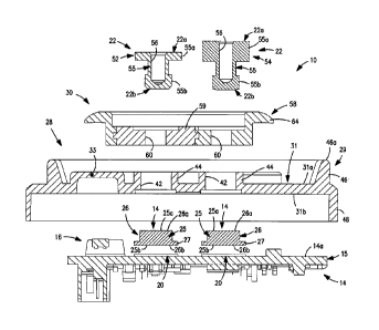
Fig. 1 is an exploded, perspective view of an exemplary electronic lock
incorporating a data interface assembly in accordance with the present
invention;
Fig. 2 is a cross-sectional view of the electronic lock and data interface
assembly;
2a
CA 02673344 2009-06-18
WO 2008/077043
PCT/US2007/087941
Fig. 3 is an enlarged, cross-sectional view of a central portion of the data
interface
assembly shown in Fig. 2;
Fig. 4 is an exploded, cross-sectional view of several components of the data
interface
assembly depicted in Fig. 3;
Figs. 5A and 58 are each a greatly enlarged, axial cross-sectional view of a
contact, a
conductor and a data port of a data interface assembly, each showing a
different value of a
spacing distance between the contact and data port; and
Fig. 6 is an exploded view of a preferred data port assembly of the data
interface
assembly.
DETAILED DESCRIPTION OF THE INVENTION
Certain terminology is used in the following description for convenience only
and is not
limiting. The words "right", left", "lower", "upper", "upward", "down" and
"downward"
designate directions in the drawings to which reference is made. The words
"inner", "inwardly"
and "outer", "outwardly" refer to directions toward and away from,
respectively, a designated
centerline or a geometric center of an element being described, the particular
meaning being
readily apparent from the context of the description. Further, as used herein,
the word
"connected" is intended to include direct connections between two members
without any other
members interposed therebetween and indirect connections between members in
which one or
more other members are interposed therebetween. The terminology includes the
words
specifically mentioned above, derivatives thereof, and words of similar
import.
Referring now to the drawings in detail, wherein like numbers are used to
indicate like
elements throughout, there is shown in Figs. 1-6 a data interface assembly 10
for an electronic
device 12, the device 12 preferably being an electronic lock (as shown) or a
data reader (not
depicted) and including a base 14 and a control 16 mounted on the base 14,
preferably on a base
mounting surface 14a. The base 14 is preferably a printed circuit board or
"PCB" 15 with front
and rear mounting surfaces 15a, 15b, but may be any other appropriate
electronic substrate, as
discussed below. The data interface assembly 10 basically includes at least
one and preferably
two contacts 20, most preferably conductive pads, mounted on the base 14 and
coupled with the
control 16, at least one and preferably two data ports 22 each having an outer
end 22a configured
to receive data from a key K (Fig. 2) with stored data and/or to transmit data
to an external data
3
CA 02673344 2009-06-18
WO 2008/077043
PCT/US2007/087941
storage device (e.g., of a lock programming or auditing device), and at least
one and preferably
two conductors 24. Each conductor 24 has a body 26 with a first end 26a
disposed against the
data port inner end 22b and a second end 26b disposed against the contact 20.
As such, the key
data DK is transmissible from the port 22, through the conductor 24 and the
contact 20 and to the
control 16, as indicated in Figs. 5A and 5B. The conductor body 26 is either
generally
compressed between, or at least generally compressible between, the data port
22 and the contact
20, for reasons described below.
Preferably, the conductor 24 is formed of a conductive carbon material and is
configured
to snub electrostatic discharge proximal to the data port 22, and thus
distally from the base 14, as
discussed in greater detail below. Further, the interface assembly 10 also
preferably comprises a
generally fluid impermeable cover 28 disposed at least partially over the base
mounting surface
14a so as to generally cover the control 16 and the contact 20, with each
conductor body 26
being at least partially disposed within the cover 28. The cover 28 is
configured to generally
prevent moisture or other fluid from contacting the control 16, the contact
20, and any other
electrical components on the base 14, as described below. Furthermore, the
interface assembly
10 preferably also comprises a support member 30 spaced from the base 14 and
configured to
retain the data port(s) 22 spaced from the associated contact(s) 20, each data
port 22 being either
molded to or connected with the support member 30 as discussed in further
detail below. Also,
the electronic device 12 preferably further includes a housing or escutcheon
32 having a front
end 32a and an interior chamber 33, the various components of the preferred
lock assembly
being disposed within, attached to, or otherwise connected with the housing
32. Specifically, the
base 14 is coupled with the housing 32 such that the control 16 and the
contact 20 are generally
disposed within the housing interior chamber 33, and the data ports 22 are
connected with the
housing front end 32a, preferably by means of the support member 30 being
connected with the
housing 32 so as to be spaced from the base 14.
Referring particularly to Figs. 5A and 5B, the data port 22 is spaced from the
contact 20
by a distance ds, which is preferably established by the spacing between the
support member 30
and the base 14. The spacing distance ds has a value lin (e.g., vi, v2, etc.)
within a range of
values; in other words, the actual value of the spacing distance ds between
the data port 22 and
the contact 20 in a specific interface assembly 10, as compared with other
data assemblies 10
(e.g., in a production run), may vary due to the tolerance "stackup" of the
various parts that the
4
CA 02673344 2009-06-18
WO 2008/077043
PCT/US2007/087941
form the interface assembly and the electric device 12, as described in more
detail below.
Therefore, with the preferred conductor body 26, the conductor 24 is
configured to provide a
conductive path Pc between the data port 22 and the contact 20 at each one of
the various
spacing distance values võ. That is, the preferred compressible conductor body
26 is compressed
to a greater or lesser extent as necessary to accommodate differences in the
spacing distance ds,
such that each one of a plurality of data assemblies 10 will function
correctly even though the
spacing distance ds of the assemblies 10 varies within the range of values.
For example, Fig. 5A
depicts one interface assembly 10 with a first, lesser spacing distance value
vi and Fig. 5B
depicts another interface assembly 10 with a second, greater spacing distance
value v2. With
both interface assemblies 10, the body 26 of each conductor 24 compresses as
required to
provide the conductive path Pc between the data ports 22 and the associated
contacts 20.
As indicated in Figs. 3, 5A and 5B, a further benefit of having a compressible
body 26 is
that the conductor 24 is configured to form a first, generally fluid
impermeable seal SI between
the body first end 26a and the data port 22 and a second, generally fluid
impermeable seal S2
between the body second end 26b and the contact 20. In other words, the
compression of the
body 26 forces the body ends 26a, 26b tightly against the associated data port
22 and contact 20,
respectively, which substantially prevents any fluid from entering
therebetween. Therefore, not
only are there reliable electrical contacts between the conductor 18 and both
the data port 22 and
the contact 20, but these electric contacts are substantially isolated from
moisture by the seals SI,
S2 formed by conductor body compression.
As best shown in Fig. 4, the conductor body 26 is preferably formed as a
generally
circular cylinder 25 (i.e., a cylinder with circular axial cross-sections)
with a radially-extending
ledge or lip 27 and arranged such that the conductor first and second body
ends 26a, 26b are
provided by the axial ends 25a, 25b of the cylinder 25. Alternatively, the
conductor body 26
may be formed of a plurality of conductive of strands or strips, commonly
referred to in the art as
"zebra stripes", as a generally pill-shaped body, as a generally tubular body,
or as any other
appropriate shape (no alternatives shown).
Regardless of the specific body shape, the conductor 24 is preferably formed
of a
combination or mixture of a conductive material and an elastic material so as
to be conductive,
compressible, and to have a degree of internal resistance, as discussed above.
Most preferably,
the conductor body 26 is formed of finely milled carbon particles or powder
mixed/milled in a
5
CA 02673344 2009-06-18
WO 2008/077043
PCT/US2007/087941
raw silicone base material, the carbon powder being in a sufficient amount or
"concentration" so
that after vulcanization or extrusion of the mixture, the body 26 is
substantially conductive. The
concentration/amount of the carbon powder in the mixture is determined by the
desired
resistance of the finished conductor 24; specifically, more carbon powder is
used when the
desired resistance of the conductor 24 is lesser, and vice-versa. Such a
material mixture is
commercially referred to as "carbon impregnated silicone". However, the
conductor body 24
may be formed of one or more other types of elastic materials, such as EPDM,
natural rubber,
etc., and/or of other types of conductive material such as copper, silver,
etc, and the scope of the
present invention embraces these and all other appropriate materials for
forming the conductor
24 so as to function generally as described herein.
In any case, being formed of a material that provides at least a degree of
resistance (i.e.,
carbon), any static electric charge accumulating at the data port 22 is
"snubbed" within the
conductor body 26, preferably generally proximal to the data port 22. As such,
electrostatic
charge is prevented from increasing or "spiking" the amplitude of any signals
(i.e., key data)
passing through the conductor 24 to the associated contact 20, which could
potentially damage
any electronic components configured to operate within a specified voltage
range. Such damage
may occur with a conductor formed of relatively highly conductive (i.e., low
resistance) material,
such as copper, steel. etc.
Referring now to Figs. 1-4, the cover 28 has a generally rectangular body 29
with a
generally thin, generally plate-like central portion 31 with front and rear
surfaces 31a, 31b, the
rear surface 3 lb being disposed generally against or upon the base 14, and is
preferably formed
of at least one sheet 33 of an elastomeric material. The elastomeric material
sheet 33 may be
natural or synthetic rubber, and is most preferably silicone rubber. With such
a cover 28, the two
preferred conductors 24 are each preferably insert molded within the
elastomeric sheet(s) 33, but
may be coupled with the cover 28 by any other appropriate technique.
Preferably, the cover 28
is provided by a portion of a flexible "keypad" that includes, and also
preferably functions to
bias, one or more input members 40 (Fig. 1) such as a pushbutton(s), input
key(s), etc., and/or
includes lights or other output members (none shown). Alternatively, the cover
28 may be
formed or constructed so as to function solely or primarily to protect the
electronic components
on the base 14 (not shown).
6
CA 02673344 2009-06-18
WO 2008/077043
PCT/US2007/087941
Referring to Figs. 3 and 4, the cover 28 preferably has at least one and
preferably a
plurality of through holes 42 each configured to receive a separate conductor
24. Preferably, the
conductor 24 is molded within the cover 28, most preferably insert molded
therewithin. The
cover 28 also preferably has one or more circular mounting flanges 44
extending outwardly from
a front surface 31a of the cover central portion 31, each flange 44 being
formed to fit tightly
about at least a portion of one conductor body 26 (i.e., insert molded about).
Further, the cover
28 also preferably has a sealing flange 46 extending outwardly from the cover
body front surface
31a and having an outer end 46a disposeable against an inner surface 32a of
the
housing/escutcheon 32. As such, the sealing flange 46 functions to
substantially prevent
moisture or other fluid from entering the space Si between the support member
30 and the base
14. Furthermore, the cover 28 also preferably includes a mounting and sealing
flange 48
extending outwardly from the cover body rear surface 31b disposeable about an
outer edge of a
base holder 17, as discussed below. The mounting and sealing flange 48 is
configured to couple
the cover 28 with the base 14 and to prevent moisture/fluid from entering the
space S2 between
the base 14 and the base holder 17, and thereby contacting electrical
components on the base rear
surface 15b, as best shown in Fig. 3.
Referring again to Figs. 1-6, the data ports 22 are preferably configured or
arranged such
that one port 22 is a data reader port 52 and the other port 22 is a ground
port 54. Preferably, the
ports 52, 54 are configured to operate as an ibutton input port (see Fig. 2)
and to alternatively
each receive a separate prong (e.g., a "banana clip") of a data reader or
programming device (not
shown). With such a structure, the reader port 52 is configured to transmit
and/or receive data
from the prongs to andior from the conductor 24, and thereafter to the control
16 or a
programming/data storage device. The ground port 54 is provided to close a
circuit including the
ibutton K or reader/programmer and the control 16. Referring particularly to
Fig. 4, each data
port 22 preferably includes a body 55 with an outer, radially larger circular
cylindrical portion
55a and an inner, radially smaller circular cylindrical portion 55b, and a
data port opening 56
sized to receive a prong, as discussed above. Further, the two ports 52, 54
are preferably
constructed such that the radially larger portion 55a of the ground port 54
has a greater axial
extent than the corresponding section of the reader port 52. As such, an
ibutton key K
contacting the reader port 52 will have a portion that contacts the ground
port 54 as required.
However, the one or more data ports 22 may be constructed in any other
appropriate manner and
7
CA 02673344 2009-06-18
WO 2008/077043
PCT/US2007/087941
the scope of the present invention is in no manner limited by the structure or
operation of the
data port(s) 22.
Referring now to Figs. 1, 3, 4 and 6, the support member 30 preferably
includes a
generally rectangular, generally disk-like body 58 connectable with the
housing 32, most
preferably frictionally retained within an opening 37 of the housing 32. The
support member
body 58 preferably has two generally circular, stepped or counter-bored
mounting holes 60 each
configured to receive and frictionally retain a separate data port 22, as
described below. Most
preferably, the support member body 58 includes a circular insert 59 providing
the mounting
hole 60 for the data port 52, as best shown in Fig. 6, but the data reader
hole 60 may alternatively
be formed in the main portion of the body 58. Further, the support body 58
preferably includes a
plurality of mounting posts 62, preferably four (only two shown), each
disposeable within a
separate mounting hole section (not shown) of the housing opening 37, and a
outer ledge or lip
64 disposeable against the housing outer surface 32a, as indicated in Fig. 4.
Preferably, the
support member 30 is formed of plastic, but may be fabricated of any
appropriate material.
Although the support member 30 is preferably constructed as described above,
the support
member 30 may be formed in any other appropriate manner.
Referring now to Figs. 1-4, as discussed above, the base 14 is preferably a
PCB 15, onto
which are mounted various electronic components used to operate the preferred
lock assembly
12. However, the base 14 may alternatively be any appropriate electronic
substrate formed of
any appropriate material such as fiber glass, glass, flex circuit, etc., or
any other electronic
assembly means capable of electrically connecting various electronic
components.
Referring particularly to Fig. 1, the preferred lock assembly 12 preferably
includes an
electronic actuator 70, preferably a motor 71 and spring shaft 72, operably
coupled with the
control 16 and configured to displace a coupling device 73, such as a
component of a clutch
mechanism 74, configured to connect a handle 75 with a retractor device 76.
Alternatively, the
actuator 70 may displace a blocking device (not shown) configured to
releasably retain the
handle 75, the retractor 76, or an intermediate connected component (not
indicated). In either
case, the control 16 is configured to receive input data from one or both data
ports 22, to
compare the input data with stored data (e.g., authorized user codes, etc.),
and to generate and
transmit a control signal to the actuator 70. The control 16 is preferably
also configured to
interface with and transmit stored data records to a data reader, for example
to provide audit
8
CA 02673344 2014-10-09
=
67363-1667
information concerning lock usage, and to receive programming instructions or
new lock codes.
However, the data interface assembly 10 of the present invention may be
configured for use with
any appropriate electronic device 12, such as for example a credential reader
for access control
systems, a generic data terminal (e.g., for ATM machines, a "watchman"
station), etc.
It is understood, that this invention is not limited to the particular
embodiments
disclosed, but it is intended to cover modifications within the scope of the
present invention
as defined in the appended claims.
9