Note: Descriptions are shown in the official language in which they were submitted.
CA 02674868 2009-07-07
WO 2008/092032 PCT/US2008/051953
1
METHOD AND APPARATUS FOR SETTING CACHE POLICIES IN A PROCESSOR
BACKGROUND
Field of the Invention
[0001] The present invention generally relates to caching operations in a
processor, and particularly relates to determining cache policies.
Relevant Background
[0002] Processor performance is improved by including one or more levels of
cache locally in a processor for storing frequently accessed or most recently
used
information. A processor cache is a small, fast memory which stores a copy of
select
information stored in main memory such as DRAM or a hard-disk drive. When an
instruction accesses a memory location, the processor first checks whether the
memory location is replicated in a local cache. Particularly, the address
associated
with the memory access is compared to all tags in a cache. If the desired
memory is
located in the cache, a cache hit occurs. Otherwise, a cache miss occurs.
[0003] When a cache hit occurs, the processor immediately reads or writes
the
information such as data or instructions in the identified cache line. In the
event of a
cache miss, the desired information is retrieved from a higher-level cache or
main
memory. Also, a new entry is conventionally allocated in the cache to store
the newly
retrieved information. The new entry comprises a tag identifying the address
that
caused the cache miss and a copy of the information retrieved from main
memory.
[0004] To accommodate a new cache entry, an existing entry is evicted from
the
cache. The heuristic used to choose the entry to evict from a cache is based
on a
replacement policy such as least recently used or first-in, first-out. Other
cache policies
(also referred to as cache attributes) are also utilized to determine how a
cache is
accessed, used and maintained. Other cache policies include write policies,
allocation
policies, cache level policies, and customized policies.
CA 02674868 2009-07-07
WO 2008/092032 PCT/US2008/051953
2
[0005] Write policies determine when information written to a cache block
is also
written to main memory. For example, cache and main memory are updated at the
same time when a write-through policy is used. When a write-back policy is
employed,
main memory is updated only when the corresponding cache block is replaced. A
write-once policy uses a write-through policy for the first write to a
particular cache
block and a write-back policy for subsequent writes to the same block.
[0006] A cache allocation policy determines when a cache block is written.
For
example, if the allocation policy associated with a particular cache block is
"allocate on
read only", the block is not disturbed during writes. To the contrary, the
cache block is
updated during both writes and reads when the allocation policy is "allocate
on read
and write". For processors having multiple levels of caches such as first-
level
instruction and data caches and at least one higher level cache, a cache level
policy
determines which level of cache is used to store information. For example,
instructions
may be stored in a first-level instruction cache while other information may
be stored
only in a second level cache.
[0007] Cache policies are conventionally stored in a page table. The page
table is
maintained in main memory with frequently accessed or most recently used
entries
being stored locally to a processor, e.g., in a Translation Lookaside Buffer
(TLB). Each
page table entry maps a virtual address to a corresponding physical address.
Particularly, a page table stores a list of virtual page numbers and
corresponding
physical page numbers. The virtual page numbers identify respective blocks of
virtual
memory allocated to processes running on a processor while the physical page
numbers identify the corresponding blocks of physical memory containing the
actual
information used by the processes.
[0008] When a processor accesses a particular memory location, page table
entries are searched using the virtual page number portion of the virtual
address
provided as part of the access. The physical page number is retrieved from the
CA 02674868 2009-07-07
WO 2008/092032 PCT/US2008/051953
3
matching page table entry. The physical page number and page offset form a
physical
address which is used to access the desired memory location.
[0009] If the desired memory location is not contained within a local
processor
cache, main memory is accessed. Cache policy information stored in the
matching
page table entry determines whether information read from or written to main
memory
as part of the memory access is stored locally in the cache, and if so, how
the
information is maintained in the cache. Thus, cache policies are
conventionally set and
applied to a cache on a per-page (or per block) basis. Further, cache policies
are
conventionally programmed by the operating system. As such, cache policies are
applied generally to all processes running on a processor and may result in
inefficiencies when utilized by a particular type of main memory device. For
example,
an "allocate on read only" cache allocation policy may optimize cache
utilization for
some processes such as graphics applications, but not others.
SUMMARY OF THE DISCLOSURE
[0010] According to the methods and apparatus taught herein, processor
caching
policies are determined using cache policy information associated with a
target memory
device accessed during a particular memory operation. Thus, caching operations
may
be tailored to particular memory device settings instead of general cache
policy
settings. Processor performance is improved by determining cache policies for
a
current memory operation based on cache policy information associated with the
target
memory device accessed during the memory operation.
[0011] According to one embodiment of a processor, the processor comprises
at
least one cache and a memory management unit. The at least one cache is
configured
to store information local to the processor. The memory management unit is
configured to set one or more cache policies for the at least one cache. The
memory
management unit sets the one or more cache policies based on cache policy
CA 02674868 2013-10-21
74769-2498
4
information associated with one or more target memory devices configured to
store
information used by the processor.
[0012] According to one embodiment of a system, the system comprises a
processor having at least one cache configured to store information local to
the
processor, one or more target memory devices coupled to the processor and a
memory management unit included in the processor. The one or more target
memory devices are configured to store information used by the processor. The
memory management unit is configured to set one or more cache policies for the
at
least one cache based on cache policy information associated with the one or
more
target memory devices.
[0012a] According to another embodiment, there is provided a method
comprising:
receiving first cache policy information at a memory management unit within a
processor, wherein the first cache policy information is received from an
address
decoder circuit based on a page table entry associated with a target memory
device
and wherein the processor is coupled to the target memory device via a memory
controller; storing the first cache policy information at the processor; and
setting the
cache policy based on second cache policy information received from the memory
controller upon receipt at the memory controller of the second cache policy
information from the target memory device; wherein the first cache policy
information
and the second cache policy information are generated by the address decoder
residing in the memory controller.
CA 02674868 2012-08-28
4a
[001213] According to another embodiment, there is provided a processor,
comprising: a cache configured to store information local to the processor;
and a
memory management unit inside the processor, the memory management unit
configured to set a cache policy for the cache based on cache policy
information
associated with a target memory device in response to receiving the cache
policy
information from a memory controller that is external to the processor and
coupled to
the target memory device; wherein the memory controller includes an address
decoder that decodes physical addresses and causes a multiplexer to select the
cache policy information associated with the target memory device.
[0012c] According to another embodiment, there is provided a system,
comprising:
a processor; a target memory device configured to store information used by
the
processor, wherein the target memory device is not a cache; and a memory
controller coupled to the processor and associated with the target memory
device,
the memory controller comprising an address decoder circuit. The processor
comprises: a cache configured to store information local to the processor; and
a
memory management unit configured to set a cache policy for the cache based on
cache policy information associated with a target memory device when the cache
policy information is available from the address decoder circuit. The memory
controller includes the address decoder that decodes physical addresses,
causing a
multiplexer to select the cache policy information associated with the target
memory
device.
CA 02674868 2012-08-28
=
4b
[0012d] According to another embodiment, there is provided a method of
determining cache policy, the method comprising: retrieving first cache policy
information associated with a target memory device; storing the first cache
policy
information at a processor that is coupled to the target memory device via a
memory
controller; and when second cache policy information is available from the
memory
controller, overwriting the stored first cache policy information with the
second cache
policy information, and setting a cache policy based on the second cache
policy
information. An address decoder located in the memory controller decodes
physical
addresses, causing a multiplexer to select the second cache policy information
associated with the target memory device.
[0012e] According to another embodiment, there is provided a processor
comprising: a cache configured to store information local to the processor;
and a
memory management unit. The memory management unit is configured to: store a
first cache policy information at the processor, wherein the first cache
policy
information is received from a page table entry associated with a target
memory
device, wherein the target memory device is not a cache and wherein the page
table
entry is identified by an address associated with a memory access by the
processor;
set a cache policy for the cache based on the first cache policy information;
and
when second cache policy information is available from a memory controller
associated with the target memory device, overwrite the stored first cache
policy
information with the second cache policy information, and replace the cache
policy
with another cache policy based on the second cache policy information. The
CA 02674868 2012-08-28
4c
memory controller includes an address decoder that decodes physical addresses
and generates a control signal that enables a multiplexer to select the second
cache
policy information.
[0012f] According to another embodiment, there is provided a system
comprising:
a target memory device; a memory controller associated with the target memory
device, the memory controller comprising an address decoder circuit; and a
processor coupled to the memory controller. The processor includes a cache
configured to store information local to the processor, and a memory
management
unit configured to: store first cache policy information at the processor,
wherein the
first cache policy information is received from a page table entry associated
with the
target memory device and wherein the page table entry is identified by an
address
associated with a memory access by the processor; set a cache policy for the
cache
based on the first cache policy information; and when second cache policy
information is available from the memory controller, overwrite the stored
first cache
policy information with the second cache policy information and set the cache
policy
based on the second cache policy information. The second cache policy
information
is provided by a multiplexer enabled by a control signal generated by the
address
decoder residing in the memory controller.
[0013] Of course, the present invention is not limited to the above
features and
advantages. Those skilled in the art will recognize additional features and
advantages upon reading the following detailed description, and upon viewing
the
accompanying drawings.
CA 02674868 2012-08-28
4d
BRIEF DESCRIPTION OF DRAWINGS
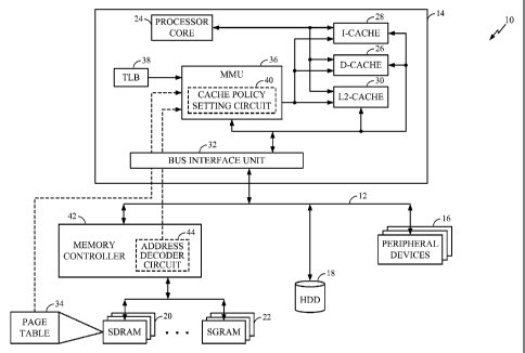
[0014] Figure 1 is a block diagram illustrating an embodiment of a
system
including a processor having circuitry for determining cache policies.
[0015] Figure 2 is a block diagram illustrating an embodiment of an
address
decoder circuit for providing cache policy information associated with a
memory
device.
[0016] Figure 3 is a block diagram illustrating another embodiment of a
system
including a processor having circuitry for determining cache policies.
[0017] Figure 4 is a block diagram illustrating an embodiment of
circuitry for
determining cache policies in a processor.
[0018] Figure 5 is a logic flow diagram illustrating an embodiment of
program
logic for determining cache policies in a processor.
[0019] Figure 6 is a diagram illustrating how the circuitry of Figure 4
determines
caching policies responsive to an exemplary write operation.
CA 02674868 2009-07-07
WO 2008/092032
PCT/US2008/051953
[0020] Figure 7 is a diagram illustrating how the circuitry of Figure 4
determines
caching policies responsive to an exemplary read operation.
CA 02674868 2009-07-07
WO 2008/092032 PCT/US2008/051953
6
DETAILED DESCRIPTION
[0021] Figure 1 illustrates an embodiment of a system 10 including a bus 12
coupling a processor 14 to one or more peripheral devices 16 and main memory
such
as a hard-disk drive (HDD) 18 and DRAM such as Synchronous DRAM (SDRAM) 20
and Synchronous Graphics RAM (SGRAM) 22. The processor 14 includes a processor
core 24, data and instruction caches 26, 28, a second-level cache (L2) 30 and
a bus
interface unit 32. The processor core 24 provides centralized control of
instruction flow
and instruction execution. The data and instruction caches 26, 28 store data
and
instructions, respectively. The L2 cache 30 provides a high-speed memory
buffer
between the data and instruction caches 26, 28 and main memory external to the
processor 14 such as the HDD 18, SDRAM 20, and SGRAM 22. The bus interface
unit
32 provides a mechanism for transferring data, instructions, addresses, and
control
signals between the processor 14 and devices external to the processor 14 such
as
peripherals 16 and main memory 18, 20, 22.
[0022] Main memory 18, 20, 22 is represented as virtual memory to processes
running on the processor 14. That is, pages of physical memory are allocated
as
virtual memory for use by processes during program execution. A page table 34
is
maintained in main memory 18, 20, 22, e.g., as shown in Figure 1, for enabling
mapping between virtual and physical address spaces. A Memory Management Unit
(MMU) 36 included in the processor 14 accesses the page table 34 and handles
memory accesses issued by the processor 14, including virtual memory
management,
memory protection, cache control, and bus arbitration. As part of virtual
memory
management, the MMU 36 maintains frequently or recently referenced page table
entries (PTEs) local to the processor 14, e.g., in a Translation Lookaside
Buffer (TLB)
38.
[0023] When the processor 14 accesses a desired memory location identified
by a
virtual address, the MMU 36 accesses the TLB 38 to determine whether the TLB
38
CA 02674868 2009-07-07
WO 2008/092032 PCT/US2008/051953
7
contains a matching entry. If so, the virtual address is translated into a
physical
address using address translation information stored in the matching TLB
entry.
Otherwise, the page table 34 is searched for a matching entry. Either way, the
MMU
36 initiates a cache lookup operation in one of the physically-tagged caches
26, 28, 30
based on the resulting physical address. If one of the caches 26, 28, 30
contains the
desired memory location, the corresponding cache line is accessed and the
memory
access completes, e.g., by reading from or writing to the cache line.
Otherwise, the
MMU 36 initiates a memory access to main memory 18, 20, 22 for accessing the
desired memory location.
[0024] Main memory 18, 20, 22 is accessed by providing the physical address
which identifies the desired memory location. The memory device containing the
desired memory location is referred to herein as the target memory device.
According
to the various embodiments disclosed herein, the target memory device may
comprise
any addressable memory module, device or bank included in the system. For
example,
a target memory device may be one of the SDRAMs 20, SGRAMs 22 or other memory
device (not shown) depending on the particular process being executed by the
processor 14.
[0025] In response to an external memory access, cache policy information
associated with the corresponding target memory device is provided to a cache
policy
setting circuit 40 included in or associated with the MMU 36. The cache policy
setting
circuit 40 determines the cache policy settings for the current memory
operation based
on the cache policy information associated with the corresponding target
memory
device. This way, when the processor 14 accesses a particular external memory
location, cache policies are tailored to the corresponding target memory
device
containing the desired memory location.
[0026] For example, if a memory operation is directed to one of the SGRAM
devices 22, the cache allocation policy associated with the target SGRAM
device may
CA 02674868 2009-07-07
WO 2008/092032
PCT/US2008/051953
8
be "allocate on read only" when the target device functions as a video frame
buffer for
a multimedia application. The processor 14 may write frequently to the target
SGRAM
device during execution of a multimedia application, but rarely read from the
device.
Thus, the target SGRAM device's cache allocation policy may indicate "allocate
on
read only" for improving processor performance. The target memory device's
cache
policy information may also indicate a particular replacement policy, write
policy,
allocation policy, cache level policy, and/or one or more customized policies.
[0027] In one embodiment, cache policy information associated with a target
memory device is provided by a memory controller 42 that provides an interface
between the bus 12 and the various DRAM devices 20, 22 as shown in Figure 1.
According to this embodiment, the memory controller 42 includes an address
decoder
circuit 44 for decoding physical memory addresses provided by the processor 14
as
part of memory accesses (e.g., reads or writes). The cache policy information
generated by the address decoder circuit 44 is a function of the physical
memory
address provided as part of a particular memory access. The physical address
identifies the memory device containing the memory location which is the
target of the
current memory operation.
[0028] Figure 2 illustrates one embodiment of the address decoder circuit
44.
According to this embodiment, the decoder circuit 44 includes an address
decoder 46,
a multiplexer 48 and a table 50 having various entries 52 associated with
respective
memory devices 20, 22 supported by the memory controller 42. Each table entry
52
contains cache policy information associated with a corresponding memory
device.
[0029] When the processor 14 accesses external memory, the physical address
included as part of the access identifies one of the memory devices 20, 22
supported
by the memory controller 42. The address decoder 46 decodes the physical
address,
causing the multiplexer 48 to select the entry 52 containing the cache policy
information associated with the target memory device identified by the
physical
CA 02674868 2009-07-07
WO 2008/092032 PCT/US2008/051953
9
address. The memory controller 42 provides the selected cache policy
information to
the MMU 36 via the bus 12 and the bus interface unit 32 (e.g., as shown by the
dashed
line going from the address decoder circuit 44 to the MMU 36 in Figure 1). The
cache
policy setting circuit 40 uses the received cache policy information to set
the cache
polices for the current memory operation. This way, cache policies may be set
on a
per-cache line basis as a function of target memory device.
[0030] In another embodiment, cache policy information is provided by an
address
decoder circuit 54 included in the processor 14 as shown in Figure 3.
According to this
embodiment, the address decoder circuit 54 provides cache policy information
based
on virtual addresses or physical addresses, e.g., as previously described and
in
accordance with Figure 2. In yet another embodiment, one or more of the memory
devices 20, 22 supported by the memory controller 42 store their cache policy
information, e.g., in a device ID register or other register (not shown). When
a target
memory device is accessed by the memory controller 42, cache policy
information is
provided to the controller 42 and forwarded to the processor 14 as previously
described. Alternatively, the cache policy information is provided to the
processor 14
without solicitation, e.g., automatically during system boot or upon reset of
the
processor 14. Further, the processor 14 may store the tailored cache policy
information upon receipt, thus obviating the need to request the same
information when
the corresponding target memory device is subsequently accessed. Instead, the
processor 14 internally retrieves and uses the tailored cache policy
information.
Regardless, the cache policy setting circuit 40 uses target memory device
cache policy
information to set cache policies during memory operations.
[0031] Figure 4 illustrates an embodiment of the cache policy setting
circuit 40
included in or associated with the MMU 36. According to this embodiment, the
cache
policy setting circuit 40 includes selection circuitry 56 for setting cache
policies directed
to a current memory operation. In more detail, a page table entry (PTE) 58
matching
CA 02674868 2009-07-07
WO 2008/092032 PCT/US2008/051953
the virtual address provided as part of a memory access is retrieved from
either the
TLB 38 or page table 34 (e.g., as shown by the dashed line going from the page
table
34 to the MMU 36 in Figure 1). The virtual address is translated into a
corresponding
physical address based on address translation information 60 stored in the
matching
PTE 58 where the physical address identifies the desired memory location.
[0032] If the desired memory location is not located in one of the
processor caches
26, 28, 30, the MMU 36 initiates an external memory access. In response to the
request, the memory controller 42 identifies the target memory device
containing the
desired memory location based on the translated physical address. The
processor 14
gains access to the target memory device via the memory controller 42. The
target
memory device performs the desired memory operation (e.g., a read or write).
In
addition, cache policy information associated with the target memory device is
provided
to the cache policy setting circuit 40 and stored in a buffer 62 as part of
the memory
operation, e.g., as illustrated by Step 100 of Figure 5.
[0033] The selection circuitry 56 processes cache policy information 64
retrieved
from the matching PTE 58 and the target memory device's cache policy
information
stored in buffer 62, e.g., as illustrated by Step 102 of Figure 5. The cache
policy
information 64 retrieved from the matching PTE 58 is overwritten with the
target
device's information and used as the current cache policy settings. However,
if no
cache policy information is provided for the target memory device, the cache
policy
information 64 retrieved from the matching PTE 58 is used instead.
[0034] A purely illustrative example of how the cache policy setting
circuit 40
determines caching policies is illustrated in Figure 6. The processor core 24
issues a
memory write request to virtual address X. The MMU 36 retrieves the matching
PTE
from either the TLB 38 or page table 34 and uses it to convert virtual address
X to a
corresponding physical address X'. The MMU 36 then probes one or more of the
physically-tagged caches 26, 28, 30 using physical address X'. In this
example, none
CA 02674868 2009-07-07
WO 2008/092032
PCT/US2008/051953
11
of the caches 26, 28, 30 contains the desired memory location as indicated by
a cache
miss. Accordingly, the MMU 36 issues an external memory write request to the
memory controller 42 based on physical address X'. The memory controller 42
selects
the target memory device containing the memory location identified by physical
address X'. The target memory device performs the desired write operation and
informs the controller 42 that the write is complete.
[0035] Additionally, the physical address X' is decoded and cache policy
information corresponding to the target memory device retrieved as previously
described, e.g., by address decoder circuit 44 or 54. Alternatively, the
target memory
device provides its cache policy information to the memory controller 42.
Regardless,
the MMU 36 is notified that the write operation has completed. Further, the
cache
policy setting circuit 40 is provided the target memory device's cache policy
information. In this example, the cache policy information indicates "allocate
on read
only." Thus, the write operation completes in the processor 14 and the MMU 36
does
not allocate a cache line in one of the processor caches 26, 28, 30.
[0036] Figure 7 continues the exemplary illustration by showing a
subsequent read
request issued by the processor core 24 to the same virtual address X. Recall,
the
target memory device's cache policy information indicates "allocate on read
only" for
the memory location identified by physical address X'. Therefore, no cache
lines were
previously allocated for physical address X'. As such, a cache miss occurs
during the
present read operation.
[0037] Further, when the target memory device completes the read operation,
the
read operation is not complete in the processor 14 because the target device's
cache
policy information indicates that a cache line should be allocated. Thus, the
cache
policy setting circuit 40 sets the current cache allocation policy such that
the MMU 36
instructs one of the processor caches 26, 28, 30 to allocate a cache line for
the
physical address X'. Additionally, a cache level policy associated with the
target
CA 02674868 2009-07-07
WO 2008/092032
PCT/US2008/051953
12
memory device may indicate which level of cache should allocate a cache line,
e.g.,
one of the first level caches 26, 28 or the L2 cache 30. Other cache policies
may also
be set based on the target device's cache policy information. Regardless, the
corresponding data is also provided to the processor core 24 for processing.
[0038] With the above range of variations and applications in mind, it
should be
understood that the present invention is not limited by the foregoing
description, nor is
it limited by the accompanying drawings. Instead, the present invention is
limited only
by the following claims and their legal equivalents.