Note: Descriptions are shown in the official language in which they were submitted.
CA 02675083 2009-08-11
DEVICE AND PROCESS INVOLVING PINHOLE UNDERCUT AREA
BACKGROUND OF THE INVENTION
100011 In recent years, there have been tremendous interest in organic thin
film
transistors (OTFTs), which promise applications such as RFID tags and liquid
crystal
displays, because fabricating OTFTs using solution processes such as spin-
coating and
jet-printing represents a low-cost manufacturing option compared to
conventional costly
photolithography. A desirable gate dielectric for OTFTs should have a very low
gate
leakage current (pinhole free) and high capacitance. To achieve high device
yield, a
considerable dielectric thickness (e.g., >500 nm) is typically used to reduce
pinhole
density, thus gate leakage current to an acceptable level. To achieve high
capacitance, on
the other hand, a thin dielectric layer (e.g., <300 nm) is preferred, since
solution
processable polymeric gate dielectrics usually have low dielectric constants.
Therefore,
there is a need for processes to make a thin dielectric layer having both high
device yield
and low gate leakage. However, OTFTs with a thin gate dielectric typically
have high
leakage and low yield due to pinholes. Thus, there is a need addressed by
embodiments
of the present invention for new electronic devices and new electronic device
fabrication
methods where the deleterious effects of pinholes are reduced.
[00021 The following documents provide background information:
[00031 Takehiro, US Patent 7,176,071 B2.
SUMMARY OF THE DISCLOSURE
[00041 In embodiments, there is provided an electronic device fabrication
method
comprising: (a) providing a dielectric region and a lower electrically
conductive region,
wherein the dielectric region includes a plurality of pinholes each with an
entry and an
exit; and (b) depositing an etchant for the lower electrically conductive
region into the
pinholes that undercuts the pinholes to create for a number of the pinholes an
CA 02675083 2011-09-01
overhanging surface of the dielectric region around the exit facing an
undercut area of the
lower electrically conductive region wider than the exit.
[0005] In other embodiments, there is provided an electronic device
comprising: (a) a
dielectric region including a plurality of pinholes each with an entry and an
exit; and (b) a
lower electrically conductive region, wherein at least some of the pinholes
are undercut with
an overhanging surface of the dielectric region around the exit facing an
undercut area of the
lower electrically conductive region wider than the exit.
[0006] In further embodiments, there is provided a thin film transistor
comprising:
(a) a dielectric region including a plurality of pinholes each with an entry
and an exit; and (b)
a lower electrically conductive region, wherein at least some of the pinholes
are undercut
with an overhanging surface of the dielectric region around the exit facing an
undercut area
of the lower electrically conductive region wider than the exit.
[006a] According to an aspect of the present invention, there is provided an
electronic
device comprising: (a) a dielectric region including a plurality of pinholes,
each pinhole
having an entry and an exit; (b) an upper electrically conductive region over
the dielectric
region, and comprising an upper electrically conductive region material; and
(c) a lower
electrically conductive region under the dielectric region, wherein at least
some of the
pinholes are undercut with an overhanging surface of the dielectric region
around the exit
facing an undercut area of the lower electrically conductive region wider than
the exit; and
wherein the upper electrically conductive region material is present in the
pinholes but in a
number of the pinholes, the upper electrically conductive region material
fails to bridge the
undercut area to contact the lower electrically conductive region.
[006b] According to another aspect of the present invention, there is provided
a thin
film transistor comprising: (a) a dielectric region; (b) an upper electrically
conductive region
over the dielectric region; (c) a lower electrically conductive region below
the dielectric
region; and (d) a plurality of pinholes in the dielectric region, each pinhole
having an entry
and an exit, and each. pinhole extending between the upper electrically
conductive region and
the lower electrically conductive region; wherein at least some of the
pinholes are undercut
with an overhanging surface of the dielectric region around the exit facing an
undercut area
of the lower electrically conductive region wider than the exit; and wherein
no electrical
connection is made between the lower electrically conductive region and the
upper
electrically conductive region through the at least some of the pinholes.
2
CA 02675083 2011-09-01
[006c] According to yet another aspect of the present invention, there is
provided a
thin film transistor comprising: (a) a dielectric region; (b) an upper
electrically conductive
region over the dielectric region; (c) a lower electrically conductive region;
and (d) at least
one pinhole in the dielectric region, the pinhole having an entry and an exit,
and extending
between the upper electrically conductive region and the lower electrically
conductive region;
wherein the at least one pinhole is undercut with an overhanging surface of
the dielectric
region around the exit facing an undercut area of the lower electrically
conductive region
wider than the exit; and wherein no electrical connection is made between the
lower
electrically conductive region and the upper electrically conductive region
through the at least
one pinhole.
BRIEF DESCRIPTION OF THE DRAWINGS
[0007] Other aspects of the present invention will become apparent as the
following
description proceeds and upon reference to the following figures which are
representative
embodiments:
[0008] FIG. I represents a first embodiment of the present invention in the
form of a
TFT;
[0009] FIG. 2 represents a second embodiment of the present invention in the
form of
a TFT;
[0010] FIG. 3 represents a third embodiment of the present invention in the
form of a
TFT;
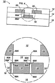
[0011] FIG. 4 represents an enlarged view of a portion of the TFT of FIG. 1;
[0012] FIG. 5 represents an enlarged view of a portion of the TFT of FIG. 2;
and
[0013] FIG. 6 represents an enlarged view of a portion of the TFT of FIG. 3.
2a
CA 02675083 2009-08-11
[0014] Unless otherwise noted, the same reference numeral in different Figures
refers to the same or similar feature.
DETAILED DESCRIPTION
[0015] The term "region" can be any suitable configuration such as a single
layer
or two or more layers of the same or different composition, where the two or
more layers
can be coterminous such as a dual-layer dielectric structure or partially
coterminous such
as a semiconductor layer contacting a source electrode and a drain electrode.
[0016] The phrase "lower electrically conductive region" refers to a
semiconductor region and/or a number of electrodes (e.g., one, two, or more
electrodes).
[0017] The phrase "upper electrically conductive region" refers to a
semiconductor region and/or a number of electrodes (e.g., one, two, or more
electrodes).
[0018] The pinhole undercut area approach can be used with any suitable
electronic device. The phrase "electronic device" encompasses for instance the
following: (1) electronic components such as for example a thin film
transistor, a
capacitor, and the like; and (2) electronic systems including such electronic
components
(e.g., transistor and/or capacitor) such as for example displays, imaging
devices, sensors,
and the like.
[0019] In embodiments, a thin film transistor typically comprises three
electrodes
(a gate electrode, a source electrode and a drain electrode), a dielectric
region (for
example, a gate dielectric), a semiconductor region, a supporting substrate,
and an
optional protecting region.
[0020] FIGS. 1-6 are illustrative embodiments of suitable thin film transistor
structural configurations. FIGS. 1-6 are merely illustrative of possible
configurations for
the various layers of a thin film transistor and are not intended to be
limiting in any
manner.
[0021] Although specific terms are used in the following description for the
sake
of clarity, these terms are intended to refer only to the particular structure
of the
3
CA 02675083 2009-08-11
embodiments selected for illustration in the drawings, and are not intended to
restrict or
limit the scope of the disclosure.
[0022] In FIG. 1, there is schematically illustrated an organic thin film
transistor
("OTFT") configuration 10 comprised of a substrate 16, in contact therewith a
metal
contact 18 (gate electrode) and a layer of a gate dielectric 14 on top of
which two metal
contacts, source electrode 20 and drain electrode 22, are deposited. Over and
between the
metal contacts 20 and 22 is a semiconductor layer 12 as illustrated herein.
Pinhole 90A
and undercut area 96A are shown.
[0023] FIG. 2 schematically illustrates another OTFT configuration 30
comprised
of a substrate 36, a gate electrode 38, a source electrode 40 and a drain
electrode 42, a
gate dielectric 34, and a semiconductor layer 32. Pinhole 90B and undercut
area 96B are
shown.
[0024] FIG. 3 schematically illustrates an additional OTFT configuration 70
comprised of substrate 76, a gate electrode 78, a source electrode 80, a drain
electrode 82,
a semiconductor layer 72, and a gate dielectric 74. Pinhole 90C and undercut
area 96C
are shown.
[0025] FIGS. 4-6 depict pinhole (90A, 90B, 90C) with entry (92A, 92B, 92C) and
exit (94A, 94B, 94C), the undercut area (96A, 96B, 96C), and the overhanging
surface
(98A, 98B, 98C).
[0026] For simplicity, in FIGS. 1-6, no upper electrically conductive region
material is depicted in the pinhole and undercut area.
[0027] In some embodiments of the present disclosure, an optional protecting
layer may also be included. For example, such an optional protecting layer may
be
incorporated on the top of each of the transistor configurations of FIGS. 1-3.
The
protecting layer may comprise for example silicon oxide, silicon nitride,
poly(methyl
methyacrylate), polyester, polyimide, or polycarbonate, or a mixture there.
[0028] Dielectric Region
4
CA 02675083 2009-08-11
[0029] The dielectric region also can be referred to as an insulating region.
In
embodiments involving for instance a thin film transistor, the dielectric
region can be
referred to as a gate dielectric. The dielectric region can be composed of
organic and/or
inorganic materials. Illustrative examples of inorganic materials suitable for
the
dielectric region include silicon oxide, silicon nitride, aluminum oxide,
barium titanate,
barium zirconium titanate and the like; illustrative examples of organic
polymers for the
dielectric region include polyesters, polycarbonates, poly(vinyl phenol),
polyimides,
polystyrene, poly(methacrylate)s, poly(acrylate)s, epoxy resin and the like.
In
embodiments, the dielectric region includes polymeric dielectric material(s).
The
dielectric region can be formed by any suitable methods such as plasma
enhanced
chemical vapor deposition, sputtering, liquid deposition methods including
spin coating,
dip coating, bar coating, printing such as ink jet, screen, flexography, and
gravure
printing. In preferred embodiments, the dielectric region is formed by liquid
deposition
methods. The thickness of the dielectric region is, for example from about 10
nm to
about 1000 nm depending on the dielectric constant of the dielectric material
used. A
representative thickness of the dielectric region is from about 100 nm to
about 500 nm.
The dielectric region may have a conductivity that is for example less than
about 10"12
S/cm or less than about 10"10 S/cm.
[0030] The dielectric region may be a single layer or may be multilayered.
Each
layer of the single layer/multilayer gate dielectric has a thickness of for
example from
about 5 nanometers to about 1 micrometer. In other embodiments each layer of
the single
layer/multilayer dielectric region has a thickness of for example from about
100
nanometers to about 1 micrometer. The thickness can be determined by known
techniques such as ellipsometry and profilometry.
[0031] Substrate
[0032) The substrate may be composed of for instance silicon, glass plate,
plastic
film or sheet. For structurally flexible devices, a plastic substrate, such as
for example
polyester, polycarbonate, polyimide sheets and the like may be preferred. The
thickness
CA 02675083 2009-08-11
of the substrate may be from about 10 micrometers to over about 10 millimeters
with an
exemplary thickness being from about 50 to about 100 micrometers, especially
for a
flexible plastic substrate and from about 1 to about 10 millimeters for a
rigid substrate
such as glass plate or silicon wafer.
[0033] Electrodes
[00341 The gate electrode can be a thin metal film, a conducting polymer film,
a
conducting film made from conducting ink or paste, or the substrate itself can
be the gate
electrode, for example heavily doped silicon. Examples of gate electrode
materials
include but are not restricted to aluminum, gold, silver, titanium, copper,
chromium,
indium tin oxide, conducting polymers such as polystyrene sulfonate-doped
poly(3,4-
ethylenedioxythiophene) (PSS-PEDOT), conducting ink/paste comprised of carbon
black/graphite or colloidal silver dispersion in polymer binders, such as
ELECTRODAGTM available from Acheson Colloids Company. The gate electrode can
be prepared by vacuum evaporation, sputtering of metals or conductive metal
oxides,
coating from conducting polymer solutions or conducting inks by spin coating,
casting or
printing. The thickness of the gate electrode ranges for example from about 10
to about
200 nanometers for metal films and in the range of about 1 to about 10
micrometers for
polymer conductors. In embodiments, the gate electrode is patterned.
100351 The source and drain electrodes can be fabricated from materials which
provide a low resistance ohmic contact to the semiconductor layer. Typical
materials
suitable for use as source and drain electrodes include those of the gate
electrode
materials such as gold, nickel, silver, aluminum, platinum, conducting
polymers and
conducting inks. Typical thicknesses of source and drain electrodes are about,
for
example, from about 40 nanometers to about 10 micrometers with the more
specific
thickness being about 100 to about 400 nanometers.
[00361 While the terms gate electrode, source electrode and drain electrode
refer
to electrodes typically used in thin film transistors, electrodes used in
other types of
6
CA 02675083 2011-09-01
electronic devices are encompassed by embodiments of the present invention
using the
electrode materials, thicknesses, and fabrication methods described herein.
[0037] Suitable electrode materials include for instance aluminum, chromium,
copper, gold, indium, nickel, platinum, silver, titanium, and a mixture
thereof.
[0038] Semiconductor Region
[0039] In embodimentsõ the semiconductor region is referred to as a
semiconductor
layer. Materials suitable for use as an organic semiconductor region include
acenes, such as
anthracene, tetracene, pentacene, and substituted pentacenes, perylenes,
fullerenes,
phthalocyanines, oligothiophenes, polythiophenes, and substituted derivatives
thereof. In
embodiments, the organic semiconductor region is formed from a liquid
processable material.
Illustrative examples of suitable semiconductor materials include
polythiophenes,
oligothiophenes, and the semiconductor polymers described in U.S. Patent
Application No.
2003/0160234, and U.S. Patent: Nos. 6,621,099, 6,774,393, and 6,770,904.
Additionally,
suitable materials include the semiconductor polymers disclosed in "Organic
Thin Film
Transistors for Large Area Electronics" by C.D. Dimitrakopoulos and P.R.L.
Malenfant, Adv.
Mater., Vol. 12, No. 2, pp. 99-117 (2002).
[0040] The semiconductor region may be formed by any suitable means including
but
not limited to vacuum evaporation, spin coating, solution casting, dip
coating, stencil/screen
printing, flexography, gravure, offset printing, inkjet-printing, micro-
contact printing, a
combination of these processes, and the like. In embodiments, the
semiconductor region is
formed by a liquid deposition method. In embodiments, the semiconductor region
has a
thickness of from about 10 nanometers to about 1 micrometer. In further
embodiments, the
semiconductor region has a thickness of from about 30 to about 150 nanometers.
In other
embodiments the semiconductor region has a thickness of from about 40 to about
100
nanometers.
[0041] The gate dielectric, the gate electrode, the semiconductor region, the
source
electrode, and the drain electrode are formed in any sequence. In embodiments
the gate
electrode and the semiconductor region are both in contact with the gate
dielectric, and the
source electrode and the drain electrode are both in contact with the
semiconductor region.
The phrase "in any sequence" includes sequential and simultaneous formation.
For example,
the source electrode and the drain electrode can be formed simultaneously or
sequentially.
7
CA 02675083 2011-09-01
The composition, fabrication, and operation of field effect transistors are
described in Bao et
al., US Patent 6,107,117.
100421 Undercut Area
100431 Any suitable etchant for the lower electrically conductive region may
be used.
The etchant more rapidly etches the lower electrically conductive region than
the dielectric
region (that is, preferential etching of the lower electrically conductive
region). In
embodiments, there is insignificant or no etching by the etchant on the
dielectric region.
Representative etchants include the following: acid such as HF, HNO3, HC1,
H2SO4, and
acetic acid, base such as KOH, NaOH, and NH3OH, H202, (NH4)2S204, and the
mixture
thereof. For example, different metals can be etched with different
combination of above
etchants. The following Table 1 summarizes typical etchants for common metals.
100441 Table I ("Hot" refers to a temperature above about 50 degrees C)
Metal Etchant Ratio (Vol) Remarks
Aluminum H20/HF 1:1
Aluminum HCl/HNO3/HF 1:1:1
Antimony H20/HC1/HNO3 1:1:1
Antimony H2O/HF/HNO3 90:1:10
Bismuth H2O/HF 10:1
Chromium H20/H202 3:1
Copper H20/HNO3 1:5
Gold HC 1 /HNO3 3:1 Hot
Indium HC 1 /HNO3 3:1 Hot
Iron H2O/HC 1 1:1
Nickel HNO3/Acetic acid/acetone 1:1:1
8
CA 02675083 2009-08-11
Nickel HF/HNO3 1:1
Platinum HCl/HNO3 3:1 Hot
Silver NH3OH/H202 1:1
Titanium H20/HF/HNO3 50:1:1
Titanium H20/HF/H202 20:1:1
[00451 Commercially available etchants such as the etchants from Transene
Company
Inc. and their compatibility with metals are listed in the following Table 2.
[00461 Table 2
Etchants Al Au Cr Cu Ni Si Si3N4 Si02 Ti W GaAs Ta/TaN
Aluminum etch ok etch etch etch surf slight ok ok ok etch surf ox
A ox
Aluminum etch ok slight ok ok ok slight ok ok ok ok ok
D
Chromium etch ok etch etch etch surf ok ok ok ok etch surf ox
Etch 1020 ox
Chromium etch ok etch etch slight ok ok ok etch ok etch ok
Etch
CRE-473
Chromium etch ok etch etch etch surf ok ok ok ok etch surf ox
Etch TFD ox
Copper etch ok slight etch etch ok ok ok slight ok etch ok
Etch 100
Copper etch ok slight etch etch ok ok ok slight ok etch ok
Etch 200
Copper ok ok ok etch etch ok ok ok ok slight NA ok
Etch APS-
100
GE-8110 etch etch ok corrode ok ok ok ok ok ok etch ok
GE-8111 etch etch ok corrode ok ok slight ok ok ok etch ok
GE-8148 etch etch ok corrode ok ok ok ok ok ok etch ok
Gold Etch etch etch ok corrode slight ok ok ok ok ok etch ok
TFA
9
CA 02675083 2009-08-11
Nichrome etch ok etch etch etch surf ok ok ok ok etch surf ox
Etch TFC ox
Nichrome etch ok etch etch etch surf ok ok ok ok etch surf ox
Etch TFN ox
Nickel etch ok etch etch etch surf ok ok ok ok etch surf ox
Etch TFB ox
Nickel etch ok ok ok etch ok ok ok ok ok ok ok
Etch TFG
Nickel etch ok slight etch etch ok ok ok slight ok etch ok
Etch Type
I
Silver etch etch ok corrode slight ok ok ok ok ok etch ok
Etch TFS
Tantalum etch ok etch etch etch etch ok etch etch ok etch etch
Nitride
Etch III
Tantalum etch ok etch etch etch etch ok etch etch ok etch etch
Nitride
SIE-8607
Titanium etch ok etch ok ok ok etch etch etch ok ok ok
Etch TFT
Titanium etch ok etch slight slight ok ok ok etch ok etch ok
Etch
TFTN
Ti- ok ok ok etch slight ok ok ok slight slight etch ok
Tungsten
Ti W-30
Tungsten etch ok etch ok ok slight ok slight ok etch etch A
Etch TFW
wherein etch = significant attack, slight = slight attack, ok = no attack ,
surf ox = only
attack surface oxidation, corrode =surface corrosion.
100471 The etchant can etch through the entire thickness or only a portion of
the
thickness of the lower electrically conductive region, where the removed
section of the
lower electrically conductive region corresponds to the undercut area. For
example,
where the lower electrically conductive region comprises both the
semiconductive layer
CA 02675083 2009-08-11
and electrodes, the etchant can etch through one or both of the semiconductor
layer and
electrodes. In embodiments, the lower electrically conductive region functions
as a
component of the electronic devices such as gate electrode of thin film
transistors. The
undercut area is only a small portion of the lower electrically conduction
region;
therefore, after undercut, the lower electrically conductive region can still
function
properly. In one example, after the undercut process, the lower electrically
conductive
region is still a continuous region, but with small holes in the region. In
other words, the
present process will not separate the lower electrically conductive region
into parts. In
embodiments, the surface area for all undercut areas in the lower electrically
conductive
region is less than about 20% of the surface area of the lower electrically
conductive
region (prior to formation of the undercut area), or less than about 5% of the
surface area
of the lower electrically conductive region (prior to formation of the
undercut area). The
phrase "surface area" refers to the surface of the lower electrically
conductive region
parallel to and in contact with the dielectric region.
[00481 Any suitable wet etching process can be used in the invented process.
For
example, the conventional wet etching process used in photolithographic
process can
used in this invention. The etching can be deposited by any method such as
blanket
coating or patterned deposition via printing on the dielectric. The device
comprising the
lower electrically conductive region and the dielectric region can be dipped
or immersed
in the etchants to perform the etching process. The etchant materials and
material
combinations, the compatibility of electrically conductive materials and the
etchants, the
concentration of etchants, and the etchant time are dependent on the lower
electrically
conductive material itself. In embodiments, there occurs etching of the lower
electrically
conductive materials with minimum side effect on the dielectric materials. In
particular,
the etchant time can be for example from about 1 second to about 1 hour, or
from about 5
seconds to about 10 min. or from about 1 second to 60 seconds. The
concentration of one
component of the etchant can be for example from about 1 percent to about 90
percent by
volume. The etching process can be performed at any suitable temperature for
example
from room temperature to about 80 degrees C, or from room temperature to about
50
11
CA 02675083 2009-08-11
degrees C, or at room temperature. To etch dual layers of lower electrically
conductive
region, two or more different etchants may be used. For example one etchant
can be used
to etch the semiconductor layer and another etchant can be used subsequently
to etchant
the electrodes.
[0049] The cross-sectional dimension (parallel to the dielectric region) of
the
undercut area is in embodiments for example from about 500 nanometers to about
4
micrometers, or from about 800 nanometers to about 2 micrometer. The depth of
the
undercut area (perpendicular to the dielectric region) ranges for example from
about 50
nanometers to about 1 micrometer, or from about 50 nanometers to the thickness
of the
entire lower electrically conductive region. In contrast, the cross-sectional
dimension
(parallel to the dielectric region) of the pinholes is typically nanometer
sized ranging for
example from about 1 to about 500 nanometers. The ratio of the cross-sectional
dimension of the undercut area to the thickness of the dielectric region is
for example
from 1:1 to about 20:1, or from about 1:1 to about 10:1. The undercut area in
the lower
electrically conductive region is for example at least about 5 times or at
least about 10
times wider than the size of the pinhole; thus, there is no connection between
the lower
electrically conductive region and the upper electrically conductive region
when the
upper electrically conductive region is deposited on the dielectric region
having the
pinholes. In embodiments, the pinholes extend through the entire thickness of
the
dielectric region where the pinholes have a depth (perpendicular to the
dielectric region)
ranging for example from about 50 nanometers to about 1 micrometer.
[0050] The benefit of the pinhole undercut area approach is that in
embodiments
the likelihood of shorting of the electronic device is reduced even with
diffusion of the
upper electrically conductive region material into the pinholes since there is
a gap (due to
the pinhole undercut area) between the upper electrically conductive region
and the lower
electrically conductive region. Thus, in embodiments, the electronic device
comprises an
upper electrically conductive region over the dielectric region wherein the
upper
electrically conductive region material is present in the pinholes but in a
number of the
12
CA 02675083 2009-08-11
pinholes the upper electrically conductive region material fails to bridge the
undercut area
to contact the lower electrically conductive region. Regarding the electronic
device
fabrication method, in embodiments, the method comprises forming an upper
electrically
conductive region over the dielectric region wherein the upper electrically
conductive
region material enters the pinholes but in a number of the pinholes the upper
electrically
conductive region material fails to bridge the undercut area to contact the
lower
electrically conductive region.
[00511 In embodiments, the lower electrically conductive region comprises a
semiconductor region and a number of electrodes. In embodiments, the upper
electrically
conductive region comprises a semiconductor region and a number of electrodes.
[00521 In embodiments, the electronic device is a transistor array having a
failure
rate that is less than about 5% due to dielectric failure. The dielectric
failure can be
determined by measuring the gate leakage, which is a current flow between the
source
and the gate electrode (IGS). For example, if the gate leakage is higher than
certain value
such as 1 nA, the off current of the transistor would be higher than this
value as well. If
the off current of a transistor is higher than specification of off current of
a transistor
array, this transistor will be considered as a defect or failure. Typically, a
backplane for
display has a transistor array comprising more than 1000 transistors, or more
than 10,000
transistors, or more than 1,000,000 transistors, or from about 1000
transistors to about 10
million transistors, depending on the display size and resolution. To improve
yield of
backplane, there is a need a method to reduce failure rate of transistors.
Dielectric failure
is one of the major reasons for transistor failure. In embodiments, the
transistor array has
a failure rate is less than about 3% due to dielectric failure, or less than
1% due to
dielectric failure.
[00531 In embodiments, the thin film transistor exhibits an improvement in the
current on/off ratio of at least about 10 times, or at least about 100 times,
or from about
times to about 10,000 times, comparing to a transistor without the undercut
using
etching. In embodiments, the thin film transistors exhibits an reduction in
gate leakage
13
CA 02675083 2009-08-11
current by at least about 10 times, or at least about 100 times, or from about
10 times to
about 10,000 times, compared to a transistors without using etching to form
the undercut
in the lower electrically conductive region. In embodiments, the thin film
transistor
exhibits an off current at least 10 times or at least 100 times, or from about
10 times to
about 10,000 times, lower than the transistors without using etching to form
the undercut
in the lower electrically conductive region.
[00541 The invention will now be described in detail with respect to specific
representative embodiments thereof, it being understood that these examples
are intended
to be illustrative only and the invention is not intended to be limited to the
materials,
conditions, or process parameters recited herein. All percentages and parts
are by weight
unless otherwise indicated. As used herein, room temperature refers to a
temperature
ranging for example from about 20 to about 25 degrees C.
[00551 Comparative Example 1 (Capacitor)
[0056] A copper layer about 200 nm in thick was deposited on glass substrate
by
vacuum evaporation. A dielectric composition was formulated by mixing 0.08 g
poly(4-
vinyl phenol) (PVP), 0.08 g poly(melamine-co-formaldehyde) (methylated, 84 wt%
in n-
butanol) as crosslinker for PVP, and 0.1 g poly (methyl silsesquioxane)
(pMSSQ) (25
wt% in n-butanol) in 0.9 g n-butanol. After filtered with 0.2 micron syringe
filter, the
dielectric composition was spin coated on top of the copper layer at 2000 rpm
for 60 s.
After dried at 80 C for 10 min, the dielectric layer was thermally annealed
and
crosslinked at 160 C for 30 min. Twenty (20) capacitors were made by
evaporating gold
electrodes on top of the dielectric layer through shadow mask. Using a
capacitor meter,
the yield of capacitor was determined to be less than 30 %.
[00571 Example 1 (Capacitor)
[00581 The copper layer (lower electrically conductive region) and the
dielectric
were prepared similar to Comparative Example 1. After crosslinking the
dielectric layer,
the device was dipped into O.1M (NH4)2S204 water solution for 2 min to
undercut the
copper layer through pinholes in the dielectric layer. After etching, the
dielectric was
14
CA 02675083 2011-09-01
washed with distilled water, isopropanol, and dried. The undercut area was
first examined
with a microscope. One clearly saw the pinhole where the underneath copper
layer was
etched away so that light passed through it. Twenty (20) capacitors were made
by
evaporating gold electrodes (upper electrically conductive region) on top of
the dielectric
layer through shadow mask. The yield was determined to be 100%.
[0059] Comparative Example 2 (Transistor)
[0060] Bottom-gate, top-contact thin film transistors were fabricated on glass
substrate. Copper (-200 nm) was evaporated as gate electrodes. The gate
dielectric was
formed on the copper gate similar to Comparative Example 1. A polythiophene
having the
following formula was used as the semiconductor:
C12H25
S S
S S
D'In
H25(G12
where n is a number of from about 5 to about 5,000. This polythiophene and its
preparation
are described in Beng Ong et al., US Patent No. 6,770,904. The polythiophene
semiconductor
layer was deposited on top of the gate dielectric on glass substrate by spin
coating. The
semiconductor layer was dried in a vacuum oven at about 80 C for 30 min and
annealed at
140 C for 10 minutes, and then cooled down to room temperature. Subsequently,
a set of
gold source/drain electrode pairs were vacuum evaporated on top of the
resulting
semiconductor layer through a shadow mask to form a series of thin film
transistors with
various dimensions.
[0061] The resulting transistors were evaluated using a Keithley 4200
Semiconductor
characterization system. Thin film transistors with channel lengths of about
90 micron and
channel widths of about 1000 microns were characterized by measuring the
output and
transfer curves. All transistors exhibited poor performance. Only 20%
transistors showed
gate modulation. Off current of the transistors were high at the level of
about 10-7 A, due to
high gate leakage through the pinholes. Current on/off ratio of the
transistors was less than
100.
10062] Example 2 (Transistors)
CA 02675083 2011-09-01
[0063] The transistors were fabricated in a way similar to Comparative Example
2,
except that etching was added. After thermal crosslinking the gate dielectric
layer, the device
was first dipped into O.1M (NH4)2S204 water solution for 2 min to undercut the
copper gate
layer through pinholes in the dielectric layer, followed by washing with
distilled water,
isopropanol, and air-drying. After depositing the semiconductor layer and
evaporated the
source/drain electrodes (the upper electrically conductive region comprise the
semiconductor
layer and the source/drain electrodes), the transistors were evaluated using a
Keithley 4200
Semiconductor characterization system. Most transistors showed good
performance. The
device yield was over 90 % with low off current at the level of 10-1 A, and
current on/off
ratio about 105. The off current was significantly lower and the current
on/off ratio was
dramatically higher than the comparative transistors
[0064] It will be appreciated that various of the above-disclosed and other
features
and functions, or alternatives thereof, may be desirably combined into many
other different
systems or applications. Various presently unforeseen or unanticipated
alternatives,
modifications, variations or improvements therein may be subsequently made by
those skilled
in the art which are also intended to be encompassed by the following claims.
Unless
specifically recited in a claim, steps or components of claims should not be
implied or
imported from the specification or any other claims as to any particular
order, number,
position, size, shape, angle, color, or material.
16