Note: Descriptions are shown in the official language in which they were submitted.
CA 02675565 2009-07-15
WO 2008/098363
PCT/CA2008/000285
NON-VOLATILE MEMORY WITH DYNAMIC MULTI-MODE OPERATION
BACKGROUND
Flash memory is a commonly used type of non-volatile memory in widespread use
as
mass storage for consumer electronics, such as digital cameras and portable
digital music
players for example. The density of a widely available flash memory chip can
be up to 4 GB
(at present) which is suitable for use in popular USB flash drives since the
size of one flash
chip is small.
The advent of 8 mega pixel digital cameras and portable digital entertainment
devices
with music and video capabilities has spurred demand for ultra-high capacities
to store the
large amounts of data, which cannot be met by the single flash memory device.
Therefore,
multiple flash memory devices are combined together into a memory system to
effectively
increase the available storage capacity. For example, flash storage densities
of 20GB may
be required for such applications. Higher density systems can be realized for
hard disk drive
(HDD) applications.
Figure 1 is a general block diagram of typical flash memory of the prior art.
Flash
memory 10 includes logic circuitry such as control circuit 12, for controlling
various functions
of the flash circuits, registers for storing address information, data
information and command
data information, high voltage circuits for generating the required program
and erase
voltages, and core memory circuits for accessing the memory array 14. The
control circuit 12
includes a command decoder and logic for executing the internal flash
operations, such as
read, program and erase functions. The functions of the shown circuit blocks
of flash memory
10 are well known in the art. Persons skilled in the art will understand that
flash memory 10
shown in Figure 1 represents one possible flash memory configuration amongst
many
possible configurations.
The memory cell array 14 of the flash memory 10 of Figure 1 consists of any
number
of banks, which is a selected design parameter for a particular flash device.
Figure 2 is a
schematic illustration showing the organization of one bank 20 of the memory
cell array 14 of
Figure 1. Bank 20 is organized into k+1 blocks, and each block consists of i+1
pages. Both k
- 1 -
CA 02675565 2009-07-15
WO 2008/098363
PCT/CA2008/000285
and i are integer values. Each page corresponds to a row of memory cells
coupled to a
common wordline. A detailed description of the memory cells of the block
follows.
Each block consists of NAND memory cell strings, having up to i+1 flash memory
cells 22 serially arranged and electrically coupled to each other.
Accordingly, wordlines
to WL, are coupled to the gates of each flash memory cell in the memory cell
string. A string
select device 24 coupled to signal SSL (string select line) selectively
connects the memory
cell string to a bitline 26, while a ground select device 28 coupled to signal
GSL (ground
select line) selectively connects the memory cell string to a source line,
such as VSS. The
string select device 24 and the ground select device 28 are n-channel
transistors.
There are j+1 bitlines 26 common to all blocks of bank 20, and each bitline 26
is
coupled to one NAND memory cell string in each of blocks [0] to [k]. Variable
j is an integer
value. Each wordline (WL0 to WL,), SSL and GSL signal is coupled to the same
corresponding transistor device in each NAND memory cell string in the block.
As those
skilled in the art should be aware, data stored in the flash memory cells
along one wordline is
referred to as a page of data.
Coupled to each bitline outside of the bank 20 is a data register 30 for
storing one
page of write data to be programmed into one page of flash memory cells. Data
register 30
also includes sense circuits for sensing data read from one page of flash
memory cells.
During programming operations, the data registers perform program verify
operations to
ensure that the data has been properly programmed into the flash memory cells
coupled to
the selected wordline. Programming within a block typically starts at the page
corresponding
to WL0, and proceeds sequentially up to WL, to fill the present block.
Alternately,
programming can start at WI., and proceed sequentially down to WL0. Then
programming
continues with WL0 of a new block. Within a device, blocks are typically
programmed in
sequence.
The flash cells of flash memory 10 can store data in one of two different
modes. Data
can be stored in a single bit per cell (SBC) storage mode or a multiple bit
per cell (MBC)
storage mode. In the SBC storage mode, exactly one bit of information is
stored in one cell to
represent one of two possible states. In the MBC storage mode, two bits are
stored in one
cell to represent one of four possible states. Of course, three bits or more
can be stored in
one cell, but the example of having two bits stored in one cell will be used
from this point
forward. The advantage of storing data in the MBC storage mode (two bits per
cell or more)
- 2 -
CA 02675565 2009-07-15
WO 2008/098363
PCT/CA2008/000285
is the at least doubling of storage capacity over the SBC storage mode when
using the same
number of cells. The main circuits of the flash memory 10 are substantially
the same when
storing data in the SBC storage mode or the MBC storage mode. Therefore, flash
memory
manufacturers apply a mask option during the fabrication process to configure
the flash
memory 10 to execute either SBC specific algorithms or MBC specific
algorithms, since the
flash circuits are controlled differently between SBC and MBC read and program
operations.
Figure 3 shows a threshold voltage (Vt) distribution graph for erased memory
cells
and programmed memory cells in the SBC storage mode. Due to process and
voltage supply
variations, the erased and programmed threshold voltages are distributed
within a voltage
range. As shown in Figure 3, erased memory cells have a negative threshold
voltage
between -3V to -1V, while programmed memory cells have a positive threshold
voltage
between 1V and 3V. The ranges depend on the desired threshold voltage for the
memory
cells. The threshold voltage ranges are illustrative of possible threshold
voltages that can be
used in a particular flash memory device, however those skilled in the art
will understand that
the selection of threshold voltages to use for erased and programmed memory
cells will
depend on the design and manufacturing process of the flash memory device.
Persons
skilled in the art will understand that different flash devices will have
different threshold
voltage ranges to suit a particular design or application.
Figure 4 shows a threshold voltage (Vt) distribution graph for erased memory
cells
and programmed memory cells in the MBC storage mode. Erased memory cells have
a
negative threshold voltage, and there are three ranges of positive threshold
voltages that the
memory cell will store, each corresponding to a different state. Preferably,
the min and max
ranges of threshold voltages for each state should be minimized, while the
spacing between
the ranges should be maximized.
It is well known that flash memory devices have a limited number of erase-
program
cycles before they can no longer be used to store data reliably. More
specifically, flash
memory cells are subject to program/erase cycle wearing, which is a
progressive
degradation of a flash memory cell due to cumulative program and erase
operations. It is
noted that a memory block is always erased first prior to being programmed
with data, hence
the cycles can be referred to as both program and erase cycles. It is the
understanding of
those skilled in the art that all currently known flash memory is configured
for block erase,
meaning that if just one page of data in a block is to be modified, the entire
block containing
that page is erased and re-programmed with the modified page and the
unmodified pages.
- 3 -
CA 02675565 2009-07-15
WO 2008/098363
PCT/CA2008/000285
The effect of such cumulative program and erase operations is the alteration
of the program
and erase characteristics of the memory cell beyond optimal parameters. When
memory
cells are degraded, higher program and erase voltages are needed to program or
erase the
memory cells to the desired threshold voltages. Eventually, the memory cells
will fail to retain
data (ie. desired threshold voltage) properly. For example, the typical rated
erase-program
cycles for current SBC flash memory is about 100,000 cycles. However, current
MBC flash
memory has a smaller rated limit 10,000 cycles. The above mentioned erase-
program cycle
limits are examples only, but it is well understood that MBC erase-program
cycles are lower
by a significant factor over SBC erase-program cycles.
Currently, most flash memory available is of the MBC type due to the large
storage
density relative to its chip size. While this is suitable for most consumer
applications, the
10,000 cycle program-erase limit may be insufficient for other applications
where data
programming and erasing is frequent. Therefore, when an MBC flash memory has
reached
its 10,000 cycle life span, it is no longer usable and must be discarded. This
problem is more
critical for commercial applications, such as HDD applications, where there
are more
frequent program-erase cycles. Because HDD applications require higher data
integrity than
most consumer applications, MBC flash memory is not suited for use due to its
relatively
short 10,000 cycle life span.
It is, therefore, desirable to provide a flash memory and flash memory system
suitable
for both consumer and commercial applications, having an extended life span.
SUMMARY
It is an aspect of the present embodiments to obviate or mitigate at least one
disadvantage of previous flash memory systems.
In a first aspect, there is provided flash memory device having a memory
array. The
flash memory device includes a command decoder, a control logic circuit, and
flash memory
circuitry for programming memory cells. The command decoder issues one of a
multiple bit
per cell (MBC) program command and a single bit per cell (SBC) program command
in
response to an external program command. The control logic circuit executes a
programming
algorithm in response to either the multiple bit per cell program command or
the single bit per
cell program command. The flash memory circuitry programs memory cells of the
memory
array in response to the programming algorithm. According to an embodiment of
the present
- 4 -
CA 02675565 2009-07-15
WO 2008/098363
PCT/CA2008/000285
aspect, the command decoder includes an SBC command decoder for issuing the
SBC
program command, and an MBC command decoder for issuing the MBC program
command.
In another embodiment of the present aspect, the memory array includes first
subdivisions configured for storing data in an MBC storage mode in response to
the MBC
program command, and second subdivisions configured for storing data in an SBC
storage
mode in response to the SBC program command. The first subdivisions and the
second
subdivisions can include memory blocks or memory pages. Each subdivision is
associated
with a mode tag for designating the MBC storage mode or the SBC storage mode,
where
each subdivision is a memory page in the memory array.
In a second aspect, there is provided a method for storing data in a flash
memory
device. The method includes converting a subdivision of the flash memory
device from a first
storage mode to a second storage mode, the subdivision having a corresponding
mode tag
indicative of either the first storage mode and the second storage mode; and
programming
the data to one of the subdivision and an alternate subdivision. According to
an embodiment
of the present aspect, the first storage mode is a multiple bit per cell (MBC)
storage mode
and the second storage mode is a single bit per cell (SBC) storage mode, and
the step of
converting is executed in response to a predetermined criteria. The
predetermined criteria is
an MBC program erase limit, and the step of converting includes comparing a
program/erase
counter corresponding to the subdivision with the MBC program/erase limit. The
step of
programming includes programming the data to the subdivision if the
program/erase counter
is less than the predetermined MBC program/erase limit, and programming the
data to the
alternate subdivision if the program/erase counter is at least the
predetermined MBC
program/erase limit. The step of programming can include erasing the
subdivision if the data
is programmed to the alternate subdivision, setting the mode tag corresponding
to the
subdivision to a state indicative of the second storage mode, or resetting the
program/erase
counter.
In another embodiment of the present aspect, the predetermined criteria is a
specific
profile of the data, where the specific profile of the data includes a set of
data file types. The
step of programming includes programming the data to the subdivision if the
data has a
profile matching the specific profile, and programming the data to the
alternate subdivision if
the profile mismatches the specific profile. In yet a further embodiment, the
subdivision
includes a block, where the block has a predetermined number of pages, or the
subdivision
- 5 -
CA 02675565 2009-07-15
WO 2008/098363
PCT/CA2008/000285
includes a page, and a predetermined number of the pages are included in a
block. In
another embodiment, the first storage mode is a single bit per cell (SBC)
storage mode and
the second storage mode is a multiple bit per cell (MBC) storage mode, and the
step of
converting includes comparing an SBC program/erase counter corresponding to
the
subdivision to a reclaim limit, and checking a state of a lock bit
corresponding to the
subdivision if the program/erase counter is less than the reclaim limit. The
step of converting
further includes changing a state of a mode tag corresponding to the
subdivision if the state
of the lock bit is false. The step of converting further includes setting the
lock bit to true after
the state of the mode tag bit is changed.
In a third aspect, there is provided a multi-mode flash memory device. The
multi-
mode flash memory device includes a memory array having flash memory cells for
storing
single bit per cell (SBC) data in an SBC storage mode and for storing multiple
bit per cell
(MBC) data in an MBC storage mode. According to embodiments of the present
aspect, a
first block of the memory array stores SBC data and a second block of the
memory stores
MBC data, or a first page in a block of the memory array stores SBC data and a
second page
in the block of the memory array stores MBC data where the first page and the
second page
each stores a mode tag, the mode tag having a logic state indicating a
presence of SBC data
or MBC data.
In a fourth aspect, there is provided a method for selectively programming
data in a
flash memory system in one of a multiple bit per cell (MBC) storage mode and a
single bit
per cell (SBC) storage mode. The method includes receiving data; determining a
high
reliability level or a low reliability level of the data; programming the data
in the SBC storage
mode if the data is determined to be high reliability; and programming the
data in the MBC
storage mode if the data is determined to be low reliability. In an embodiment
of the present
aspect, the step of programming the data in the SBC storage mode includes
programming
the data to selected SBC pages in a memory array of a flash memory device and
setting
mode tags corresponding to each of the selected SBC pages to a first state.
Furthermore,
the step of programming the data in the MBC storage mode includes programming
the data
to selected MBC pages in the memory array of the flash memory device and
setting the
mode tag corresponding to each of the selected MBC pages to a second state.
In a fifth aspect, there is provided a method for reading data from a flash
memory
system having multiple bit per cell (MBC) pages and (SBC) pages. The method
includes
- 6 -
CA 02675565 2009-07-15
WO 2008/098363
PCT/CA2008/000285
receiving a read address for reading at least one page of the flash memory
array; executing
an MBC read operation at the read address if a mode tag corresponding to the
at least one
page is in a first logic state; and executing an SBC read operation at the
read address if the
mode tag corresponding to the at least one page is in a second logic state.
The method
includes initializing an address mapping table with mode tags corresponding to
each page of
the flash memory array prior to receiving the read address. In an embodiment
of the present
aspect, the step of initializing includes powering up the flash memory array,
reading the
mode tags stored in each page of the flash memory array, and storing the mode
tags with
logical address entries corresponding to each page of the flash memory array.
Reading the
mode tags includes executing an SBC read operation for reading the mode tags
in each
page of the flash memory array. In another embodiment, the step of receiving
includes
issuing an external read command from a flash controller to a flash memory
device, the
external read command being generated in response to the read address and the
logic state
of the mode tag bit corresponding to the read address. The step of executing
the MBC read
operation can include decoding the external read command within the flash
memory device
and issuing one of an internal MBC read command and an internal SBC read
command.
Other aspects and features of the described embodiments will become apparent
to
those ordinarily skilled in the art upon review of the following description
of specific
embodiments of the invention in conjunction with the accompanying figures.
BRIEF DESCRIPTION OF THE DRAWINGS
The embodiments will now be described, by way of example only, with reference
to
the attached Figures, wherein:
Fig. 1 is a block diagram of flash memory device of the prior art;
Fig. 2 is a schematic showing the organization of one memory bank of the
flash memory device of Figure 1;
Fig. 3 is a threshold voltage (Vt) distribution graph for erased memory cells
and programmed memory cells in the single bit per cell storage mode;
Fig. 4 is a threshold voltage (Vt) distribution graph for erased memory cells
and programmed memory cells in the multiple bit per cell storage mode;
Fig. 5 is a block diagram of a multi-drop flash memory system;
Fig. 6 is a block diagram of a serially configured flash memory system;
- 7 -
CA 02675565 2009-07-15
WO 2008/098363
PCT/CA2008/000285
Fig. 7 is a flow chart of a method for extending the life span of a multi-mode
flash memory device;
Fig. 8a and 8b are illustrations of memory blocks converted between the MBC
storage mode and the SBC storage mode;
Fig. Sc and 8d are illustrations of pages converted between the MBC storage
mode and the SBC storage mode;
Fig. 9 is a diagrammatic illustration of allocated fields for one page of the
memory array;
Fig. 10 is a block diagram of a flash memory system including one multi-mode
flash memory device;
Fig. 11 is a flow chart of a method for operating the flash memory system of
Figure 10;
Fig. 12 is a flow chart of a method for initializing an address mapping table
with mode tag information;
Fig. 13 is a flow chart of a method for extending the life span of a multi-
mode
flash memory device;
Fig. 14 is a flow chart of a method for user selectable programming of MBC
and SBC storage mode data;
Fig. 15 is a flow chart of a method for automatically converting an MBC
storage mode subdivision into an SBC storage mode subdivision;
Fig. 16 is a flow chart of a method for reclaiming an SBC storage mode
subdivision; and,
Fig. 17 is a flow chart of a method for reading data from a multi-mode flash
memory device.
DETAILED DESCRIPTION
Generally, at least some example embodiments provide a method and system for
extending the life span of a flash memory device. The flash memory device is
dynamically
configurable to store data in the single bit per cell (SBC) storage mode or
the multiple bit per
cell (MBC) storage mode, such that both SBC data and MBC data co-exist within
the same
memory array. Such a memory device is referred to as a multi-mode flash memory
device.
- 8 -
CA 02675565 2009-07-15
WO 2008/098363
PCT/CA2008/000285
One or more tag bits stored in each page of the memory is used to indicate the
type of
storage mode used for storing the data in the corresponding memory block. A
controller
monitors the number of program-erase cycles corresponding to each page for
selectively
changing the storage mode in order to maximize lifespan of the multi-mode
flash memory
device.
The presently described embodiments are applicable to single MBC flash memory
devices such as the one shown in Figure 1, and a system of MBC flash memory
devices
such as the ones shown in Figures 5 and 6.
Figure 5 is a block diagram of a flash memory system 100 integrated with a
host
system 102. Flash memory system 100 includes a flash memory controller 104 in
communication with host system 102, and multiple multi-mode flash memory
devices 106.
The host system 102 will include a processing device such as a
microcontroller,
microprocessor, or a computer system. The flash memory system 100 of Figure 5
is
configured to include one channel 108, where multi-mode flash memory devices
106 are
coupled in parallel to channel 108. Those skilled in the art will understand
that the memory
system 100 can have more or less memory devices coupled to it.
Channel 108 includes a set of common buses (not shown), which include data and
control lines that are coupled to all the memory devices 106. While not shown,
each memory
device is enabled/disabled with a respective chip select signal provided by
flash memory
controller 104. The flash memory controller 104 is responsible for issuing
commands and
data, via the channel 108, to a selected memory device 106 based on the
operation of the
host system 102. Data read from the memory devices is transferred via the
channel 108 back
to the flash memory controller 104 and host system 102. Flash memory system
100 is
generally referred to as a multi-drop configuration, in which the multi-mode
flash memory
devices 106 are coupled in parallel with respect to channel 108. Those skilled
in the art will
understand that the flash memory controller 104 can have multiple channels,
each with flash
memory devices 106 coupled in the multi-drop configuration. Each multi-mode
flash memory
device 106 is implemented as NAND flash memory devices having the bank memory
organization previously shown in Figure 2. The flash memory devices 106 can
have the
same capacity or different capacities.
- 9 -
CA 02675565 2014-03-05
Figure 6 is a block diagram of a flash memory system having serially coupled
memory
devices. Flash memory system 120 includes a flash memory controller 122 in
communication
with host system 124, and four serially coupled multi-mode flash memory
devices 126. Each
of the four flash memory devices has an input/output circuit for facilitating
operation between
memory devices. An example of a such a flash memory device is described in
commonly
owned U.S. Patent Application Serial No. 11/354,023, filed on December 30,
2005, and
commonly owned U.S. Patent Application Serial No. 11/496,278, filed on July
31, 2006.
According to an embodiment, the multi-mode flash memory device is set by
default to
store data in the MBC storage mode. The life span of each multi-mode flash
memory device
is extended by executing a life span extension scheme. Figure 7 is a flow
chart illustrating a
life span extension scheme.
The first step is the cell conversion 200, typically executed in response to a
programming instruction. The program/erase cycles for all the subdivisions
configured in the
MBC storage mode are monitored, and any subdivision reaching a predetermined
limit will
automatically be converted to the SBC storage mode. A subdivision is the
smallest unit or
grouping of cells that are convertible, such as a memory block or a page, for
example. This is
due to the fact that any MBC storage mode subdivision reaching the
predetermined limit will
no longer store data reliably, but they can be used for storing data in the
SBC storage mode
for a set number of program/erase cycles. The cell conversion algorithm will
also convert
subdivisions from the SBC storage mode to the MBC storage mode, if the data
stored therein
is no longer retained.
Following at step 202, data is programmed according to the selected storage
mode.
By default all the subdivisions of the memory bank, are set to store data in
the MBC storage
mode. However, if the user elects to store data that requires higher storage
reliability, then at
least the required number of subdivisions are allocated and set for storing
the data file in the
SBC storage mode. The flash memory controller (104 or 122 for example) can be
configured
to recognize specific data file extension types as being those that require
higher storage
reliability. For example, executable applications with an ".exe" in the
Windows TM operating
system platform will be stored in the SBC storage mode while a video data file
with an ".avi"
extension does not require higher storage reliability. Therefore, the
subdivisions configured in
CA 02675565 2009-07-15
WO 2008/098363
PCT/CA2008/000285
the SBC storage mode will have a longer life span than subdivisions configured
in the MBC
storage mode.
Use of any one of the above-mentioned steps of the life span extension scheme
will
extend the life of the multi-mode flash memory device. However, maximum life
span
extension is achieved when both steps are used during operation of the multi-
mode flash
memory device.
Figures 8a and 8b graphically illustrate the conversion of subdivisions of the
memory
from the MBC storage mode to the SBC storage mode, and vice versa, where a
subdivision
is presently a memory block. For ease of illustration, the multi-mode flash
memory device
300 of Figure 8a consists of four memory blocks 302, each of the four memory
blocks
including four pages 304. It is presumed that the memory device 300 had all
its blocks 302
initially set to store data in the MBC storage mode, and has been subjected to
either the user
or the automatic cell conversion algorithms previously described in Figure 7.
Hence, by
example, the multi-mode flash memory device 300 has the configuration of SBC
and MBC
pages as shown in Figure 8a, where the shaded blocks are set to store data in
the SBC
storage mode and the non-shaded blocks are set to store data in the MBC
storage mode.
Figure 8b illustrates the mapping of the multi-mode flash memory device 300
after
pages 304 have been converted. In a first example, it has been determined that
the MBC
storage mode block containing pages 306, 308, 310 and 312 has reached a
predetermined
number of program/erase cycles. Therefore, they are converted to the SBC
storage mode.
The program/erase cycles are monitored for each page 304 in the block 302, and
block
conversion is executed when at least one of the pages reaches the
predetermined number.
In a second example, it has been determined that the SBC storage mode block
containing pages 314, 315, 316 and 317 are no longer storing data. This can be
determined
when the data therein is erased and no other data is stored therein. The
number of SBC
program/erase cycles for SBC pages 314, 315, 316 and 317 is checked, and
because at
least one of their respective SBC program/erase cycles has reached a
predetermined limit,
the entire block is converted back to the MBC storage mode. Specific details
regarding the
MBC to SBC storage mode and SBC to MBC storage mode conversion will be
discussed
later.
-11 -
CA 02675565 2009-07-15
WO 2008/098363
PCT/CA2008/000285
Figures 8a and 8b illustrate the conversion of block based subdivisions
between the
SBC storage mode and the MBC storage mode. Figures 8c and 8d illustrate the
conversion
of page based subdivisions between the SBC storage mode and the MBC storage
mode. As
shown in Figure 8c, pages 318 and 320 are set to store data in the MBC storage
mode, and
pages 322 and 324 are set to store data in the SBC storage mode. In the first
example, it is
determined by monitoring the program/erase cycles that both pages 318 and 320
have
reached the predetermined MBC program/erase cycle limit. Hence individual page
conversion to the SBC storage mode is executed. In the second example, it is
determined by
monitoring the program/erase cycles that both pages 322 and 324 have reached a
predetermined limit. Hence individual page conversion to the MBC storage mode
is
executed.
The determination of the storage mode of any block 302 in the memory device
300 is
achieved by checking a mode tag (at least one bit) stored in one of the pages
304. This
allows the memory device 300 to execute the proper programming and read
operations upon
the selected block 302. Figure 9 is a diagrammatic illustration of a page 304,
specifically
showing its allocated fields. Page 304 includes a user data field 350 and a
spare data field
352. User data field 350 stores data received from the user, while spare data
field 352 is
reserved for use by the flash device or flash memory controller. In the
present example, user
data field 350 is 2KB in size while the spare data field 352 is 64B in size.
In the spare data
field 350, one or more bits are designated as a storage mode tag 354, and
several bits are
designated as a program/erase cycle counter 356 for tracking the number of MBC
program/erase cycles executed upon the page.
An SBC counter 358 is included to track the total number of SBC program/erase
cycles executed upon the page to support SBC to MBC and subsequent MBC to SBC
conversions. One example application is to program data at high speed using
the SBC
storage mode, and then convert to MBC storage mode later to improve memory
capacity
during an idle period. An optional lock bit 360 can be provided for preventing
an SBC storage
mode page from being converted to the MBC storage mode. Further details of
this feature
will be discussed later. Although memory block 302 will include any number of
pages 304,
any one or more of the pages 304 can be selected for storing the tag bit, the
SBC counter
value, the MBC counter value and the optional lock bit corresponding to the
memory block
302.
- 12 -
CA 02675565 2009-07-15
WO 2008/098363
PCT/CA2008/000285
The mode tag 354 is used by the multi-mode flash memory device 300 to
determine
the specific read, program and erase algorithm to use. As previously
discussed, read and
program algorithms that involve setting of specific voltage levels and timing
of control signals
differ for data stored in the SBC and MBC storage modes. Such differences are
well known
to those skilled in the art. In particular, if a subdivision (such as a block,
for example) to be
read or programmed has its corresponding mode tag 354 set to a specific logic
state, then
the flash device will execute MBC storage mode algorithms. Otherwise, the
flash device will
execute SBC storage mode algorithms. Execution of the algorithms specific to
the SBC and
MBC storage modes is governed by the command decoder and logic circuits of the
multi-
mode flash memory device.
In some embodiments, the multi-mode flash memory device will include all the
circuits
and control logic required for executing operations specific to both the SBC
and MBC storage
modes. It is noted that an MBC flash memory device typically includes all the
circuits used by
an SBC flash memory device. The main difference between dedicated MBC and SBC
flash
memory devices is the control circuitry and logic circuits for executing the
algorithms.
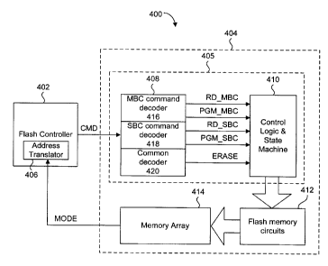
Figure 10 is a block diagram of a flash memory system including one multi-mode
flash memory device. Flash memory system 400 includes a flash memory
controller 402 and
a multi-mode flash memory device 404. While only one device 404 is shown for
convenience
of illustration, the system 400 can include any number of devices 404 coupled
to the same
channel, and the system 400 can include any number of channels. Details of the
flash
memory controller 402 and multi-mode flash memory device 404 will now be
described.
A typical component of the flash memory controller 402 is a logical to
physical
address translator 406, which is responsible for mapping each logical address
provided by
the host system to a corresponding physical address in the multi-mode flash
memory device.
As will be appreciated by those skilled in the art, address mapping is used to
ensure that the
logical address for data consistently points to its actual physical location
in the memory array
if the data is moved or reprogrammed to implement wear leveling operations.
Also, the
translator is commonly implemented as an address mapping table. According to
the present
embodiment, each mode tag (MODE) of each subdivision of the multi-mode flash
memory
device 404 is obtained and stored with its corresponding logical address entry
in the mapping
table. If the subdivision is a block, then the corresponding mode tag for the
logical addresses
corresponding to the block is stored. Alternately, if the subdivision is a
page, then the mode
- 13-
CA 02675565 2009-07-15
WO 2008/098363
PCT/CA2008/000285
tag of each page is obtained and stored. Therefore, the flash memory
controller 402 will
issue external commands (CMD) with information relating to the type of storage
mode
associated with the selected addresses.
The multi-mode flash memory device 404 shown in Figure 10 includes a multi-
mode
control circuit 405 consisting of command decoder 408 and control logic 410,
flash memory
circuitry 412 and a memory array 414. Flash memory circuitry 412 and memory
array 414
have been simplified for sake of clarity, however those skilled in the art
should understand
that these circuit blocks include all the necessary components to ensure
proper operation of
the multi-mode flash memory device 404. The command decoder 408 receives an
external
command CMD issued by the flash memory controller 402, decodes the command,
and
issues a corresponding internal control command to the control logic 410.
Those skilled in
the art will understand that the external command CMD will include information
such as the
type of operation to be executed, user data to be programmed, and an address
to which the
data is to be written to or data is to be read from. Control logic 410 is a
state machine having
logic for executing all standard SBC and MBC read and program operations,
including any
supplementary operations such as program verify operations. The control logic
410 also
includes logic circuitry for executing logical functions unique to the multi-
mode flash memory
device, as will be described later.
The command decoder 408 includes an MBC command decoder 416, an SBC
command decoder 418 and a common command decoder 420. The MBC command decoder
416 issues MBC storage mode specific commands, such as an MBC read command
RD _MBC and an MBC program command PGM_MBC. The SBC command decoder 418
issues SBC storage mode specific commands, such as an SBC read command RD_SBC
and an SBC program command PGM_SBC. The common decoder 420 issues commands
that are not specific to memory subdivisions configured for the SBC or MBC
storage modes,
such as an erase command. The three sub-command decoders 416, 418 and 420 are
shown
as distinct circuit blocks to illustrate the categorization of the types of
commands issued by
the command decoder 408, and does not necessarily indicate a specific circuit
or grouping of
logic used for generating the commands.
The general operation of flash memory system 400 is now described with
reference to
the flow chart of Figure 11. Prior to carrying out of the steps of the
illustrated operating
method, it is assumed that the mode tag information has already been loaded
into the
-14-
CA 02675565 2009-07-15
WO 2008/098363
PCT/CA2008/000285
address translator 406. Now at step 450, a host request is received, which can
include a
read or write request for example. The request will include the logical
address for writing data
to or the logical address for reading data from, the multi-mode flash memory
device 404. At
step 452 the flash memory controller 402 looks up the address mapping table
and generates
the appropriate command CMD with an indication regarding the necessary type of
storage
mode operation that is required (SBC vs MBC storage mode), based on the
requested logical
address and the state of the corresponding mode tag in the address mapping
table. The
CMD command received by the command decoder 408 is decoded, and either SBC
storage
mode or MBC storage mode read/program commands are issued at step 454 by MBC
command decoder 416 or SBC command decoder 418. Of course, the CMD command can
be a non storage mode specific command such as an erase operation that is
issued by
common command decoder 420. At step 456, the control logic 410 executes the
required
algorithm and controls the necessary multi-mode flash memory circuitry 412 in
the proper
manner.
Prior to any operation being executed by the multi-mode flash memory device
404,
the address mapping table of the flash memory controller 402 is initialized
with the mode tag.
This is preferably done during a time when there are no user operations being
executed,
such as during power up of the flash memory system 400. Figure 12 is a flow
chart
illustrating a method for initializing the address mapping table. At step 500
the flash memory
system 400 is powered up. Then at step 502, flash memory device 404 scans its
memory
array to assess the logic states of all its tag bits. This is done by
executing a read operation
of all the pages in the flash memory device 404, and providing only the mode
tag information
(MODE) to the flash memory controller 402. If an entire page of data is read
out at the same
time, only the tag bit is used and the remaining data read out from the pages
is ignored. The
address mapping table is then populated with the MODE tag data at step 504.
In order to maximize the speed and to simplify the mode tag read out process,
all the
pages are read out using the SBC storage mode read algorithm. More
specifically, the SBC
read algorithm detects the presence or absence of an erased state of the tag
bit. The two
binary logic states can be used to determine the SBC or MBC storage mode
configuration of
the subdivision (ie. block or page for example). Preferably, the flash memory
device will be
pre-programmed during manufacturing/testing to have all its mode tag bits set
to one logic
state (the erased state) indicating that data is to be programmed in the MBC
storage mode.
- 15-
CA 02675565 2009-07-15
WO 2008/098363
PCT/CA2008/000285
During standard operation, the flash memory device 402 will be subjected to
program and
erase operations, whereby eventually at least one subdivision, be it a page or
block of
memory, will have its mode tag changed.
Figure 13 is a flow chart illustrating a method for extending the life span of
multi-mode
flash memory device 400 by automatically changing the state of the mode tag.
The method
outlines specific criteria, or conditions, before a mode tag is changed. The
method starts at
step 550 where data is programmed to the multi-mode flash memory device. It is
presumed
that there is a mix of SBC storage mode subdivisions and MBC storage mode
subdivisions in
the memory array of the multi-mode flash memory device. Hence at step 550, an
SBC or
MBC programming operation will be executed.
At step 552, the number of program cycles for each subdivision of the memory
array
is monitored after a program/erase cycle. Alternately, the monitoring can be
done just prior to
a program/erase cycle. It is noted that every program operation to a
subdivision of the
memory is preceded by an erase operation at some point, hence the number of
erase cycles
or program cycles is substantially the same. The address mapping table can
include a
program/erase counter for each subdivision, which is initially populated with
a corresponding
counter value stored in the spare data field (352) of the page. The counter
values can be
loaded during power up of the system and programmed back to the page as data
is
programmed. Monitoring in step 552 includes comparing the program/erase
counter for the
currently programmed subdivision(s) with a predetermined limit. There are two
predetermined limits that are used based on the. One limit is the SBC storage
mode limit,
while the other is the MBC storage mode limit. For example, MBC storage mode
subdivisions
will have a limit of 10,000 program/erase cycles, and the SBC storage mode
subdivision will
have a limit of 100,000 program/erase cycles. Before or after the programming
operation has
been completed, the comparison is executed. Then, one of three possible
actions is taken if
the applicable predetermined limit is reached.
The first possible action is to extend the life span of MBC storage mode
subdivisions
in step 554 by converting them to the SBC storage mode. Therefore, any data
presently
stored in the MBC storage mode subdivisions to be converted is either moved or
programmed to available MBC storage mode subdivisions. Then the corresponding
mode tag
bits in the address mapping table are changed in step 556 to indicate that the
subdivisions
- 16 -
CA 02675565 2009-07-15
WO 2008/098363
PCT/CA2008/000285
are set to the SBC storage mode. The tag bit field of the page is programmed
as data is
programmed to the page.
The second possible action is to reclaim SBC storage mode subdivisions in step
558
by converting them to the MBC storage mode. This is a reverse process to the
one
.. discussed in step 554. Reclamation is done under two conditions, one being
that the number
of SBC program/erase cycles is under a predetermined value less than the
standard SBC
limit, where the standard SBC limit can be 100,000 cycles. This is due to the
fact that SBC
memory cells programmed close to 100,000 cycles will be degraded to the point
that they will
not reliably store data in the MBC storage mode. Therefore, a reduced SBC to
MBC
.. reclamation limit is used. This reduced limit is selected such that the
subdivision will reliably
endure the standard MBC limit of 10,000 program/erase cycles. In one
embodiment, the
reduced SBC to MBC reclamation limit will correspond to the MBC limit. For
example, if the
MBC limit is 10,000 cycles, then the SBC memory cells can be converted to the
MBC storage
mode provided they have endured 10,000 SBC program/erase cycles or less. The
second
.. condition is that the data stored in the SBC subdivisions is no longer
used, ie. the data has
been erased and not reprogrammed to the same subdivisions. When a subdivision
is erased,
the address mapping table is updated to indicate that the subdivision is free.
Once these two
conditions are met, the mode tag state in the address mapping table is changed
in step 556.
Therefore, it is advantageous to reclaim such SBC subdivisions for high
density storage.
The third possible action is to retire SBC subdivisions at step 560 when they
have
reached their SBC program/erase cycle limit. In this case, the subdivisions
are simply
mapped out and no longer used by the flash memory system. Mapping out of
unusable
subdivisions is a well known operation in flash memory systems. However, by
this point in
time, the subdivision(s) will have stored data in both the MBC and SBC storage
modes,
.. thereby maximizing the lifespan of the subdivision(s).
The previously described embodiments presume that the multi-mode flash memory
has all its subdivisions configured to store data in the MBC storage mode by
default.
However, any MBC storage mode subdivision can be converted to the SBC storage
mode by
the host system Figure 14 is a flow chart illustrating the method for host
system selectable
.. programming of MBC and SBC storage mode data. This method can be executed
as a sub-
routine of step 550 in the life span extension method of Figure 13. Starting
at step 600, the
flash memory controller will receive a programming instruction from the host
and identifies
-17-
CA 02675565 2009-07-15
WO 2008/098363
PCT/CA2008/000285
the type of data to be programmed. The type of data can be image files such as
JPEG's,
various application data files such as spreadsheet or text documents, and
executable
programs, for example. Since each file will have a specific extension, the
flash memory
controller will identify the specific data type. The flash memory controller
then determines if
the data file requires high reliability in step 602. This can be done for
example, by checking a
table that includes all the data types considered to require high reliability.
For example,
executable programs can be considered to require high reliability. It is noted
that the host
system can pre-select the data types requiring high reliability.
If the data type does not appear in the table, then the method proceeds to
step 604,
and the multi-mode flash memory device programs the data in the MBC storage
mode. More
specifically, the flash memory controller identifies free subdivisions having
a mode tag set to
the MBC storage mode from its address mapping table, and issues the
appropriate MBC
programming command to the multi-mode flash memory device. Upon receiving the
command, the multi-mode flash memory device will proceed with internal
programming
operations in the manner previously described for Figure 10. Once internal
program
verification has determined that the data has been successfully programmed,
the
program/erase counters in the address mapping table corresponding to the
selected pages
are incremented at step 606.
Returning to step 602, if the data type does appear in the table, then the
method
proceeds to step 608 where the flash memory controller checks if there are
free SBC storage
mode subdivisions available. If free SBC storage mode subdivisions are
available, then the
multi-mode flash memory device is instructed to program the data into the
corresponding
physical locations in the SBC storage mode at step 610. Otherwise, the
necessary MBC
storage mode subdivisions are converted to the SBC storage mode in step 612 by
inverting
the state of their mode tag. Then step 610 is executed to program the data in
the SBC
storage mode. Following SBC storage mode programming at step 610, the
corresponding
program/erase counters are incremented at step 606. Therefore, the user
selectively
programs data in either the MBC or SBC storage modes in the multi-mode flash
memory
device.
The previously discussed method categorized data file types as being either
the high
or low reliability type. In an alternate embodiment, the data file types can
be categorized into
-18-
CA 02675565 2009-07-15
WO 2008/098363
PCT/CA2008/000285
different reliability levels. Then the host system can set a threshold for
determining which
reliability levels are to be categorized as high reliability data.
As previously discussed, the flash memory system can automatically execute the
life
span extension algorithms. Figure 15 is a flow chart illustrating one method
for automatically
converting an MBC storage mode subdivision into an SBC storage mode
subdivision. A
programming instruction is first received by the flash memory controller at
step 650. For
example, the programming instruction is to modify an existing file stored in
the same
subdivisions of the multi-mode flash memory device. The program/erase counter
for the
selected subdivision(s) is compared to the predetermined cycle limit for the
MBC storage
mode at step 652. If the counter value is less than the limit, then the data
is simply
programmed to the same subdivisions in the multi-mode flash memory device at
step 654.
Otherwise, the limit has been reached and the data is programmed to new
subdivisions at
step 656. Then the original subdivisions are erased at step 658 to clear the
data. Finally, the
states of the mode tag for the original subdivisions in the address mapping
table are inverted
at step 658, thereby designating them as SBC storage mode subdivisions. The
subdivisions
converted to the SBC storage mode will have their program/erase counters reset
at step 662,
since now there are a predetermined number of SBC program/erase cycles that
can be
executed before the subdivisions expire and can no longer be used.
An alternate modified sequence is to program the data, increment the counter
and
then compare the program/erase counter to the predetermined cycle limit. No
further action
is taken if the counter value is less than the cycle limit. Otherwise, the
recently programmed
data is moved, or reprogrammed, to available MBC storage mode subdivisions.
The
reprogramming can be done whenever the system is idle. Then the original
subdivisions are
erased and the mode tag bits are inverted.
The steps for programming data to SBC storage mode subdivisions is
substantially
the same as the one shown in Figure 15. The MBC program/erase limit is
replaced with the
SBC program/erase limit, and SBC storage mode subdivisions are simply retired
from use if
the SBC subdivision program/erase counter is equal to the SBC program/erase
limit. The
SBC data is then programmed to an available SBC storage mode subdivision. If
only MBC
storage mode subdivisions are available, then the method of Figure 14 is
executed to convert
the required MBC storage mode subdivisions to the SBC storage mode, and
program the
data.
- 19-
CA 02675565 2009-07-15
WO 2008/098363
PCT/CA2008/000285
In the above mentioned embodiment, one counter can be used for tracking MBC
program/erase cycles, and then re-used for tracking SBC program/erase cycles
when
converted to the SBC storage mode. According to an optional embodiment, if the
SBC
subdivisions can be reclaimed, then separate SBC and MBC program/erase
counters are
provided.
The method of Figure 16 outlines the steps for reclaiming an SBC storage mode
subdivision. This method can be executed at any time while the flash memory
system is
active. The method starts at step 700 by identifying each SBC storage mode
subdivision that
is empty, ie. not intended to store any data. At step 702, the SBC
program/erase counter is
compared to the MBC reclaim limit. If the counter is at least the reclaim
limit, then the
process ends at step 704 and the SBC storage mode subdivision will not be
converted to the
MBC storage mode. On the other hand, if the SBC program/erase counter is less
than the
reclaim limit, then the status of a lock bit is checked at step 706. The lock
bit being set to an
active state indicates that the current SBC subdivision has been previously
converted from
the MBC storage mode to the SBC storage mode by the automatic conversion
method of
Figure 14. In otherwords, if the SBC storage mode subdivision has already
exhausted its
MBC program/erase cycles, there is no reason to reclaim it from the SBC
storage mode for
further use as an MBC storage mode subdivision. If the lock bit is not set,
then the state of its
corresponding mode tag is changed at step 708. At step 710, the lock bit is
set to prevent
future reclaiming of this subdivision should it ever be converted back to the
SBC storage
mode.
The previously discussed methods present techniques for programming data in
the
multi-mode flash memory device, and for extending the life span of the multi-
mode flash
memory device during programming operations. In these operations, the mode tag
is used
for determining whether data is to be programmed with the MBC or SBC storage
modes, and
for executing automatic conversion between the modes. Once programmed, the
mode tag is
used for determining the type of read operation to be executed. Figure 17 is a
flow chart
outlining a method for reading data from the multi-mode flash memory device.
Starting at step 750, a read instruction is received by the flash memory
controller. The
read instruction will include a logical address of the desired data. The flash
memory
controller will then check its address mapping table for the state of the mode
tag bits
corresponding to the logical address in step 752. If the state of the mode tag
is a first state,
- 20 -
CA 02675565 2009-07-15
WO 2008/098363
PCT/CA2008/000285
such as a logic "1" for example, then a MBC storage mode read command CMD is
generated
and provided to the multi-mode flash memory device. In response, the multi-
mode flash
memory device will decode the command and issue an RD_MBC command at step 754.
The
MBC read is then executed at step 756. Otherwise, the multi-mode flash memory
device will
issue an RD_SBC command at step 758 and an SBC read is then executed at step
760.
Regardless of the specific type of read command, the data will be read out
from the memory
array and provided back to the flash memory controller. Therefore, both data
programmed in
the SBC and MBC storage modes can be accessed by the user from the same multi-
mode
flash memory device.
In all the previously discussed embodiments, the selective MBC or SBC
processes
executed by the flash memory controller and the multi-mode flash memory device
are done
transparently to the user. There are no additional instructions, or
modification of instructions
required from the user, as all determination of SBC/MBC storage mode
operations are done
by the flash memory controller. Accordingly, there is minimal overhead
required for
implementing the presently described flash memory system with a host system.
Therefore, the previously described embodiments of the multi-mode flash memory
device can be controlled to selectively program data in the SBC storage mode
or the MBC
storage mode, such that data programmed in both storage modes co-exist within
the same
memory array at the same time. The selective programming can be done under
user control
based on the type of data being programmed, and/or automatically through
preset
algorithms. By storing data with both types of storage modes, the life span of
the multi-mode
flash memory device is extended over flash memory devices dedicated to storing
data only in
the MBC storage mode. The subdivisions referred to in the previously described
embodiments can be memory banks, memory blocks or pages.
In the preceding description, for purposes of explanation, numerous details
are set
forth in order to provide a thorough understanding of the embodiments.
However, it will be
apparent to one skilled in the art that these specific details are not
required in order to
practice the embodiments. In other instances, well-known electrical structures
and circuits
are shown in block diagram form in order not to obscure the aspects of the
embodiments.
For example, specific details are not provided as to whether the embodiments
described
herein are implemented as a software routine, hardware circuit, firmware, or a
combination
thereof.
- 21 -
CA 02675565 2009-07-15
WO 2008/098363 PCT/CA2008/000285
The above-described embodiments are intended to be examples only. Alterations,
modifications and variations can be effected to the particular embodiments by
those of skill in
the art without departing from the scope, which is defined solely by the
claims appended
hereto.
- 22 -