Note: Descriptions are shown in the official language in which they were submitted.
CA 02675860 2009-07-17
WO 2008/089354 PCT/US2008/051351
PERMANENTLY DESTRUCTIBLE RESONANT CIRCUIT
WITH NON-SELF-HEALING CAPACITOR
SPECIFICATION
CROSS-REFERENCE TO RELATED APPLICATIONS
This utility application claims the benefit under 35 U.S.C. 119(e) of
Provisional
Application Serial No. 60/885,531 filed on January 18, 2007 and entitled RF
Label for
Container Stopper or Cap and Provisional Application Serial No. 60/980,948
filed on October
10, 2007 and entitled Permanently Destructible Resonant Circuit with Non-Self-
Healing
Capacitor and both of whose entire disclosures are incorporated by reference
herein.
BACKGROUND OF THE INVENTION
FIELD OF INVENTION
The present invention relates to a resonant circuit used for the prevention of
shoplifting or
the like, and more particularly, to a resonant circuit having a capacitor that
is permanently
deactivated by exposure to a predetermined voltage level.
DESCRIPTION OF RELATED ART
In retail shops, libraries or the like, a surveillance system including a
resonant tag that
resonates with a radio wave, a transmitting antenna and a receiving antenna
has been used for the
prevention of shoplifting. In an embodiment, the resonant tag is composed of
an insulating film, a
coil and a plate made of a conductive metal foil formed on one side of the
insulating film, and a plate
made of a conductive metal foil formed on the other side, which constitute an
LCcircuitandresonates
witharadiowaveataparticularfrequency. In another embodiment, the resonant tag
is composed of a
wire loop and a discrete capacitor, both of which are embedded in or affixed
to an object to be
protected from theft. An example of this type of tag includes a bottle
stopper, such as a wine
bottle stopper wherein the wire loop inductor and discrete capacitor are
connected in parallel and
installed inside the bottle stopper. Copending provisional application
60/885,531 discloses such
a device.
If an article with the resonant circuit attached passes through a surveillance
area without
being disabled at checkout, the resonant circuit resonates with the radio wave
from the transmitting
antenna, and the receiving antenna detects the resonance and generates an
alarm. A typically used
resonant frequency is 5 to 15 MHz, because frequencies within the range can be
easily distinguished
from various noise frequencies. In electric article surveillance (EAS), a
frequency of 8.2 MHz is most
popularly used, and in radio frequency identification (RFID), afiequencyof
13.56MHzismostpopulatiy
1
CA 02675860 2009-07-17
WO 2008/089354 PCT/US2008/051351
uSed.
By way of example only, Figs. 1-3 depict a prior art LC resonant circuit in
the form of a
tag 10 which includes a coil 11 and a first capacitor plate 12 on one side
(Fig. 1) of a substrate 13
and a second capacitor plate 14 on the other side of the substrate 13 (Fig.
2). Fig. 3 is a cross-
sectional view of this prior art tag showing a typical substrate thickness, t,
of approximately 20
microns, which tends to be the thinnest dielectric that can be formed using
conventional dielectric
forming methods (e.g., extruding polyethylene between the metal layers).
Adhesive layers 15 and
17 secure the metal layers to the substrate 13 respectively.
Prior art resonant tags formed as in Figures 1-4 are commonly deactivated,
once an article
with the resonant tag is purchased, by application of a predetermined voltage
to the tag. The tag
typically has a thinned part of the dielectric where the induced voltage
across the capacitor plates 12,
14 causes dielectric breakdown, thereby making the resonant tag incapable of
resonating with a radio
wave at a predetermined frequency. This means for deactivating a resonant tag
is shown in Figure 4.
Figure 4 shows a portion of a capacitor formed by upper and lower metal plates
2,3 affixed to a
dielectric 4 with adhesive layers 5A, 5B. The plates, which are typically
metal foil or the like are
dimpled 10A, l OB to form a narrowed area in the dielectric 4. When sufficient
voltage is applied to the
capacitor, a short forms across the narrowed area of the dielectric. The short
disables the capacitor and
the tag will no longer resonate. A common problem with this type of
deactivation means occurs where
the tag is incorporated into or attached to an article of clothing and must
remain deactivated for the
useful life of the clothing. Often, the dielectric, which has been shorted as
described above, heals itself
when the clothing is worn or washed. Many dielectrics are also known to heal
over time, without any
physical agitation. In resonant tags having polyethylene dielectrics, as many
as 50% of the tags become
reactivated with wearing or laundering. This unintended reactivation has
undesirable consequences for
the wearer of the clothing, who will activate security tag detection devices
when exiting any store with
equipment tuned to the tag's resonant frequency. Not only is the false alarm
inconvenient and
embarrassing for the person wearing the clothing with the reactivated tag, but
frequent false alarms can
cause a "boy who cried wolf' effect. Store personnel can become lax about
enforcement of tag alarms
when many of them are falsely triggered by reactivated tags on legitimately
purchased goods. The
inconvenience and embarrassment of false alarms may so irritate consumers that
sales of clothing
brands bearing re-activatable tags are lost.
One alternative to resolve the self-healing dielectric problem is to use a
fuseable circuit element
instead of a capacitor as the deactivation means. Resonant circuits that are
deactivated by applying a
high voltage that causes sufficient current to vaporize a fusable link are
described in U.S. Patent No.
2
CA 02675860 2009-07-17
WO 2008/089354 PCT/US2008/051351
5,861,809. This patent and all other references in this application are
incorporated into this application
by reference. The fuesable link does not self-heal, and thus, resonant
circuits that are deactivated by this
means are permanently deactivated, with no chance of self-healing. Typically,
a fuesable link 36 is
installed in a gap in the coil portion 70 of a tag, as shown in Fig. 5. the
fuseable link can be connected to
the coil by wire bonded wires 40, 42 or by conductive epoxies or other means.
One drawback of the fuesable link is that the narrowed area in the fuse that
is designed to
destruct under high current has a relatively high resistance compared to the
rest of the circuit elements.
This increased resistance lowers the Q of the resonant circuit. Resonant
circuits with a low Q produce a
weaker resonant signal and must be placed closer to deactivation circuitry in
order to generate sufficient
current to destroy the fuse, which is burdensome for checkout personnel. Low Q
also requires that the
resonant circuit coil be physically larger to generate sufficient current for
deactivation and to be detected.
Larger circuits naturally have higher manufacturing costs and are less
desirable as they are more
difficult to conceal in merchandise to be protected.
Thus a need exists for an improved resonant circuit that can be permanently
disabled.
BRIEF SUMMARY OF THE INVENTION
An object of the present invention is to provide a resonant circuit mainly
used in a radio-wave
detection system for the prevention of shoplifting or the like that is
permanently disabled by
application of a predetermined voltage which causes permanent breakdown of a
capacitor located
in the circuit.
As a result of earnest study, the inventors have found that the object
described above can
be attained if a ceramic capacitor or other form of capacitor having a
predetermined breakdown
voltage at which permanent dielectric breakdown results is included in the LC
circuit of the
resonant circuit, and achieved the present invention.
Briefly, the present invention is as follows. A resonant tag resonates with a
radio wave at a
predetermined frequency and comprises: an inductor, which can be a coil formed
in essentially
two dimensions and made of a metal foil or printed with a conductive material
or a wire loop
inductor, and a ceramic or other non-reversible dielectric capacitor having a
predetermined
breakdown voltage, such that, once that voltage is exceeded, the capacitor is
permanently
disabled, thus permanently disabling the LC resonant circuit.
In another embodiment, a resonant circuit resonates with a radio wave within a
predetermined
resonant frequency range. The resonant circuit includes an inductor; and a
capacitor having a
predetermined dielectric breakdown voltage. The inductor and capacitor form an
LC circuit and
the resonant circuit is permanently disabled by inducing a voltage to the
capacitor that exceeds
3
CA 02675860 2009-07-17
WO 2008/089354 PCT/US2008/051351
the predetermined breakdown voltage. The capacitor dielectric can be made of a
ceramic, metal
oxide or mineral substances.
Another embodiment is a circuit element adapted for use in a resonant circuit.
The
circuit element is in the form of a strap having two electrically conductive
ends. The
electrically conductive ends are connected to each other by a dielectric
material forming a
capacitor having a predetermined breakdown voltage. The dielectric material
can be made of a
ceramic, metal oxide or mineral substances.
BRIEF DESCRIPTION OF SEVERAL VIEWS OF THE DRAWINGS
The invention will be described in conjunction with the following drawings in
which like
reference numerals designate like elements and wherein:
Fig. 1 is an enlarged plan view of one side of a prior art resonant tag;
Fig. 2 is an enlarged plan view of the other side of the prior art resonant
tag of Fig. 1;
Fig. 3 is a cross-sectional view of the prior art resonant tag taken along
line 3-3 of Fig.
1;
Fig. 4 is a cross-sectional view of a narrowed area in a prior art resonant
tag;
Fig. 5 is a prior art planar resonant circuit with a fuesable link;
Fig. 6 is a plan view of an exemplary resonant tag with wire-bonded ceramic
capacitor;
Fig. 7 is a cross-sectional view of the wire-bonded ceramic capacitor of Fig.
6;
Fig. 7a is a cross sectional view of a surface mount ceramic capacitor;
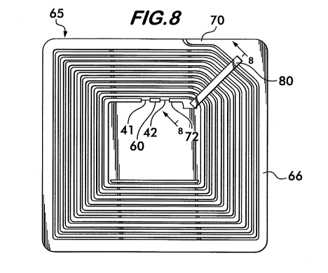
Fig. 8 is a plan view of an exemplary resonant circuit with a conductive
strap;
Fig. 8a is a cross-sectional view of an exemplary conductive strap installed
on the
resonant circuit of Fig. 8 and taken along line 8-8;
Fig. 9 is a plan view of an exemplary resonant tag having a ceramic capacitor
mounted
on a strap;
Fig. 10 is a cross-sectional view of the tag of Fig. 9 taken along line 10-10
of Fig. 9;
Fig. 11 is a plan view of an exemplary capacitor strap for use in a resonant
tag;
Fig. 12 is cross-sectional view of the capacitor strap of Fig. 11, taken along
line 2-2;
Fig. 12a is a cross-sectional view of another version of the capacitor strap
of Fig. 11
taken along line 2-2,
Fig. 12b is a cross-sectional view of a capacitor strap having an insulating
layer on the
bottom;
4
CA 02675860 2009-07-17
WO 2008/089354 PCT/US2008/051351
Fig. 13 is a plan view of an exemplary resonant tag having a capacitor strap
as in Figs.
11-12;
Fig. 14 is a cross-sectional view of the tag of Fig. 13 taken along line 14-
14;
Fig. 15 is an exploded view of a resonant circuit for use in a bottle stopper;
Fig. 16 is a cut-away view of a resonant circuit in a bottle stopper.
DETAILED DESCRIPTION OF THE INVENTION
In an exemplary embodiment, an LC resonant circuit 65 is formed on a
substantially
planar substrate as shown in Figs. 6 and 7. The frequency (f) at which the LC
circuit resonates
is determined by the values of L and C in the following equation:
1
f 2;r LC
In this embodiment, the capacitor 60 is a chip capacitor with contacts 61
suitable for wire
bonding. An inductor is formed by a coil 70 of conductive material, which can
be metal foil, a
printable conductive material or like means known in the art. In order for the
tag to form a
closed LC circuit, the open end of the inductor coil 70 and the metal foil
connected to the open
end of the capacitor 72 must be connected together. Means for achieving this
are known in the
art, and include, a separate conductor on the underside of the tag that
connects the two ends 70
and 72. In this embodiment, the conductors on the top and bottom sides of the
tag are separated
by an insulation material, which can also be a substrate for the tag. The
insulation material is
pierced in order to made electrical contact between the upper and lower
layers. Such an
embodiment is shown in prior art Fig. 3, where conductive material 11, 12 on
the top side of the
tag is adhered to an insulator material 13 with an adhesive 15 and conductive
material 14 is
adhered to the bottom side of the insulator material 13 with an adhesive 17.
Connection between the open inductor end 70 and the open capacitor end 72 can
also be
by a separate conductive strap 80 installed on top of the conductive material
of the tag 65, as
shown in Fig. 8. and 8a. The separate conductive strap 80 has exposed ends 82
and 83 that
make direct contact with the ends 70 and 72 of the conductor. The conductive
strap also has
electrical insulation 81 that covers the area where the strap crosses traces
70a-j of the inductor.
The conductive strap is electrically connected at its ends 82, 83 to the
conductive material of the
tag 70, 72. This can be by hot or cold welding, conductive epoxy or other like
means known in
the art. These modes of attachment and the use of a strap in particular are
disclosed in co-
CA 02675860 2009-07-17
WO 2008/089354 PCT/US2008/051351
pending U.S. Patent Application No. 11/539,995.
An alternate embodiment for connecting the capacitor to the conductive
elements of the
tag, is shown in Fig. 7a. In this embodiment, the capacitor 60 is a capacitor
that is in the form
suitable for surface mount attachment, having solder bumps 63 on its
underside. The solder
bumps are made to electrically and physically bond the capacitor to the
conductive material 70,
72 of the tag. Surface mount devices and means for establishing electrical
connections with
solder bumps are well known in the art.
The capacitor has the following features. The capacitor must be non-self
healing upon
dielectric breakdown. Typical dielectric materials include ceramic, metal
oxides and minerals
such as mica. In a preferred embodiment, the dielectric has a breakdown
voltage of 3-10 volts
DC. In a preferred embodiment, the dielectric has a total thickness of 60 -
2000 angstroms. In
a preferred embodiment, the resonant circuit formed as described above has a Q
of between 55
and 90.
In a further embodiment, the capacitor is attached to a strap-like device
similar to that
described above and in co-pending application 11/539,995. Figs. 9-10 depict
the use of the strap
19 with a chip capacitor 15 attached, being used on a coil 10A to form an LC
resonant tag. A
chip capacitor includes capacitors formed on a silicon substrate. The
capacitor strap 19 is
electrically coupled to the coil at points 25D, 25C in a manner similarly
discussed with regard to
Figs. 8 and 8a, including attachment means such as hot and cold welding and
conductive epoxy.
The capacitor strap 19 comprises a capacitor 15 that is electrically connected
to conductive
flanges 19A and 19B. A gap 19G separates these two flanges to prevent shorting
the capacitor
15 electrical contacts (not shown). The conductive flanges 19A and 19B are
electrically coupled
to respective locations 11, 12 of the coil 10A at connections 25C and 25D,
respectively. To
prevent shorting the capacitor 15 to coil elements 13, 14 when the capacitor
strap 19 is
electrically coupled to the coil 10A, an insulating layer 19C (e.g., paper) is
disposed between the
conductive flanges 19A/19B and the coil 10A, as shown most clearly in Fig. 10.
A further embodiment is shown in Figures 11-13. In this embodiment, a strap
that
connects electrically to both ends of a planar inductor as described above, is
formed with an
integral capacitor. A capacitor strap 20 is electrically coupled to an EAS or
RFID coil or antenna, by
electrically connecting the non-overlapping ends 22B of the first electrically
conductive planar element
22 and the non-overlapping end 24B of the second electrically conductive
planar element 24 to
respective portions of the coil or antenna. The capacitor strap is a thin
component for electrically
bridging at least two respective portions of an antenna or coil component of
an EAS or RFID tag
6
CA 02675860 2009-07-17
WO 2008/089354 PCT/US2008/051351
or inlay. The strap component exhibits a desired capacitance and has a
predictable breakdown
voltage range that causes irreversible breakdown. The capacitor strap
comprises a first
electrically conductive planar element 22 and a second electrically conductive
planar element
24, and a planar dielectric layer 24A, 22A disposed between at least portions
of the first and
second electrically conductive planar elements.
The first electrically conductive 22 element includes a first portion arranged
to be
secured in electrical continuity with one of the at least two respective
portions of the antenna or
coil. The second electrically conductive element 24 includes a first portion
arranged to be
secured in electrical continuity with another of the at least two respective
portions of the antenna
or coil, resulting in the formation of the EAS or RFID tag or inlay. A
capacitor formed in this
manner, but with a flexible polymer dielectric is described in co-pending U.S.
Patent
Application No. 11/539,995 filed on October 10, 2006, which is incorporated
herein by
reference.
Fig. 11 depicts an enlarged plan view of a capacitor strap 20. As can be seen
most clearly in
Fig. 12, the capacitor strap 20 comprises a first electrically conductive
planar element 22 having an
associated ceramic dielectric layer 22A and a second electrically conductive
planar element 24 having
an associated ceramic dielectric layer 24A and wherein portions of the
elements 22 and 24 overlap 26,
thereby forming a capacitor. As is known to those skilled in the art, the
amount of overlap 26 deterrnines
the capacitance. The dielectric must be such that once the capacitor breakdown
voltage is exceeded, the
capacitor cannot self-heal. Exemplary dielectric materials include ceramics,
metal oxides and minerals.
A capacitor strap 20 is electrically coupled to an EAS or RFID coil or
antenna, by elect.rically
connecting the non-overlapping ends 22B of the first electrically conductive
planar element 22 and the
non-overlapping end 24B of the second electrically conductive planar element
24 to respective portions
of the coil or antenna. Where the coil or antenna comprises several turns, for
example as shown by the
coi110 in Fig. 13, in order to prevent shorting of the second electrically
conductive planar element 24,
an insulator layer 28 (Fig. 12A, e.g., a dielectric material), or paper
insulator layer 28A (Fig. 12B), is
applied to the element 24, or is otherwise interposed between the second
electrically conductive planer
layer 28 and the coil/antenna. As can be most clearly seen in Fig. 14, the
insulator layer 28 isolates the
element 24 from turn tracks 13 and 14, while electrical connection of the
capacitor strap 20 is made at
connections 25A and 25B at ends 22B and 24B of the capacitor strap 20 to coil
tracks 11 and 12,
respectively. It should be noted that where a coil of less than one turn is
provided, the insulator layer 28
is not required since the capacitor strap 20 does not crossover any other coil
tracks. Thus, an EAS tag or
inlay 16 is created having an equivalent circuit formed by the coil 10 and the
capacitor strap 20.
7
CA 02675860 2009-07-17
WO 2008/089354 PCT/US2008/051351
In a further embodiment, shown in Figs. 15 and 16, a deactivatable resonant
circuit 120
is positioned within a stopper or cap of a bottle or container. In particular,
the resonant circuit
120 comprises an RF wound coil and permanently deactivatable capacitor that
resonates
preferably at (but is not limited in any way to) 8.2 MHz. However, unlike
existing RF wound
coil/capacitor circuits, the circuit 120 is permanently deactivatable with
conventional
deactivation equipment (e.g., Checkpoint's COUNTERPOINT deactivator
equipment).
Fig. 15 depicts an exemplary bottle closure 102 (e.g., Zork cork or wine
closure
manufactured by Zork Pty Ltd of Australia) that can house the deactivatable
resonant circuit
120 of the present invention. In particular, the closure comprises a stopper
104 comprising a
cavity 106 into which the deactivatable resonant circuit 120 is positioned and
secured therein
(e.g., using an adhesive or a plurality of fingers, etc., that are present on
the inner wall of the
cavity 106). A seal 108 is sealed over the opening to the cavity 106. The
stopper 104 is then
positioned inside the opening of the bottle B (Fig. 16) and then a cap cover
110 with a tear-away
portion is applied around the bottle top, thereby completing the bottle
closure 102. Fig. 16 is an
enlarged view of the top of an exemplary bottle B having the bottle closure
102 applied thereto
and shown in cross-section to reveal the placement of the deactivatable
resonant circuit 120
therein. It should be understood that the circuit 120 shown in Figs. 15-16 is
not limited to the
circuit shown but includes any of the embodiments disclosed in the instant
application and any
equivalents thereof.
As mentioned previously, the deactivatable resonant circuit 120 of the present
invention
is not limited to bottle closures but may be used in container closures (caps,
lids, etc. where
cavities are provided therein). In addition, the deactivatable resonant
circuit 120 may be
positioned in other retail items where the circuit 120 can be concealed
without a tactile detection
(e.g., lining or collars of coats, padding, etc.).
The RF wound coil/capacitor circuit 120 comprises an LC circuit as described
herein
where the wound coil is an inductor (L) and a capacitor (C) is connected to
each end of the coil.
The inductor is created using a thin wire (aluminum or copper) with an
insulating layer
(preferable polyethylene) to prevent shorting of the coil
To make the RF wound coil/capacitor circuit 120 deactivatable, the circuit
comprises a
capacitor with a dielectric breakdown voltage in the range of 3 to 10 volts
DC. A ceramic
capacitor can be used or any other permanently deactivatable capacitor with
the appropriate
breakdown voltage. When the predetermined minimum deactivation field strength
is applied to
the LC circuit, the voltage across the capacitors plates exceeds the desired
breakdown voltage
8
CA 02675860 2009-07-17
WO 2008/089354 PCT/US2008/051351
and a short is created across the capacitor plates. The LC circuit will
therefore no longer
resonate at the proper frequency and is permanently deactivated.
It should be noted that although the figures depict EAS style security tags,
it is witliin the
broadest scope of the present invention to include RFID chips as part of the
security tag.
It should be further noted that any of the above embodiments can also be
practiced by
having two or more capacitors in series. In this case each of capacitors must
be permanently
disableable when a dielectric break down occurs to a particular capacitor, or
the dielectric
breakdown voltage of all permanently disableable capacitors in the circuit
must be lower than
the dielectric breakdown voltage of any capacitors that are not permanently
disableable. For
example, the resonant tag describe above, having an inductor formed on a
planar substrate can
also have a capacitor formed on the substrate. As noted above, however,
capacitors formed by a
conventional prior art methods have the potential to "self heal" over time
after dielectric
breakdown. Thus, for the resonant circuit to be permanently disabled, the
capacitor that breaks
down must not be capable of self healing. If a ceramic capacitor (or other non-
self-healing type)
is used in series with a self-healing capacitor, and the ceramic capacitor has
a guaranteed
breakdown voltage that is lower than that for the self-healing capacitor, then
the resonant circuit
will always be permanently disabled when exposed to a voltage sufficient to
cause breakdown in
the ceramic capacitor. Such an embodiment can be used where accurate control
of total tag
resonant frequency is desirable and the capacitor formed on the tag substrate
can be trimmed to
vary the resonant frequency, especially where the ceramic capacitor and/or the
inductor have
manufacturing tolerances that are larger than acceptable to maintain the
desired resonant
frequency. Trimming a prior art self-healing capacitor formed on a flexible
security tag
substrate by methods such as laser trimming, etching, and cutting is well
known in the art. For
example see U.S. Patent No. 7,119,685.
While the invention has been described in detail and with reference to
specific examples
thereof, it will be apparent to one skilled in the art that various changes
and modifications can be
made therein without departing from the spirit and scope thereof.
9