Note: Descriptions are shown in the official language in which they were submitted.
CA 02676207 2009-07-22
WO 2008/089787 PCT/EP2007/000567
AN ELASTOMERIC PARTICLE HAVING AN ELECTRICALLY CONDUCTING SURFACE, A PRESSURE
SENSOR COMPRISING SAID PARTICLES, A METHOD FOR PRODUCING SAID SENSOR AND A
SENSOR SYSTEM COMPRISING SAID SENSORS
Technical Field
The present disclosure relates to pressure sensors
and systems comprising such sensors. In particular, the
present disclosure is directed towards sensors and sensor
systems that may be used for measuring pressure on a body
part.
Hence, the present disclosure relates to particles
that may form part of sensor elements, sensor systems,
clusters of sensor elements and devices for measuring
pressure on a body part.
Prior Art
There are many applications in which it may be
desirable to measure pressure on a body part. As a non-
limiting example, it may be desirable to measure pressure
on a body part in connection with compression treatment
of the body part. Compression therapies may be used for
treatment and/or prophylaxis of a number of conditions,
including, but not limited to, Deep Vein Thrombosis
(DVT), vascular disorders, circulatory disorders, edemas,
heart conditions (treated by counterpulsation),
lymphedema, burns, injuries, and embolisms.
Some devices for compression treatment are known in
the art, e.g. from US 2004/0073146 Al, US 2004/0073146
Al, US 2002/0173735 Al, US 6,494,852 Bl, US 5,997,465, US
6,123,681, US 6,198,204 B1, EP 1 324 403 Al, US
2004/0167375 Al, WO 2004/093763 Al and US 2005/0043657
Al.
Presently available systems for measuring pressure
on a body part, however, suffer from a number of
drawbacks. Major issues with existing measurement systems
have been identified in the areas of mismatched
mechanical properties (body/device impedance mismatches
and resulting interface stress modification), sensitivity
CONFIRMATION COPY
CA 02676207 2009-07-22
WO 2008/089787 PCT/EP2007/000567
2
(often too high), quiescent impedance (often nearly
infinite), nonlinearity, poor repeatability (cycle to
cycle and insertion to insertion), creep, hysteresis, and
sensitivity to curvature, temperature-pressure-humidity,
etc.
Generally existing sensors have excellent precision
(which is good) and perform well at high pressures in
planar, mechanically isolated spaces between well
characterized surfaces. Such spaces and surfaces are not
available in the case of devices for measuring pressure
on a body part.
US 2,951,817 discloses a variable resistance
material, comprising a body of elastomeric polyvinyl
chloride with a granular filler selected from a group
consisting of precipitated manganese dioxide and
microphone carbon granules.
US 3,629,774 discloses a progressively collapsible
variable resistance element, comprising an elastic
cellular structure of e.g. elastomer foam. Examples given
include silicone rubber, natural rubber, latex and
polyurethane rubber. The element further comprises a
conducting coating provided on the inside of the cells in
the structure. Examples of coating materials are carbon
(graphitized, partially graphitized, carbon black),
silver, gold, copper, tungsten, aluminium, and other
metals.
US 4,292,261 discloses a pressure sensitive
conductor and method of manufacturing the same. The
conductor comprises an isolating elastomer having
electrically conductive magnetic particles dispersed
therein.
US 6,388,556 B1 discloses a film pressure sensitive
resistor and pressure sensitive sensor. The film compri-
ses a binder, spherical elastomeric particles and
conductive particles, such as carbon black. Examples of
conductive particles comprise graphite, carbon black,
indium-doped tin oxide and the like. Examples of elastic
CA 02676207 2009-07-22
WO 2008/089787 PCT/EP2007/000567
3
organic fillers comprise silicone polymer, acrylic
polymer, styrene polymer, urethane polymer and the like.
Examples of spherical elastomeric particles comprise
nylon particles. The binder may be a silicone rubber,
polyurethane resin, epoxy resin, phenol resin or
polyester resin.
US 6,291,568 B1 discloses a polymer composition
comprising an electrically conductive filler material
selected from a group consisting of powder-form metallic
elements and alloys, electrically conductive oxides of
such elements or alloys and mixtures thereof, mixed with
a non-conductive elastomer.
The above described sensors are of a conductive
elastomer type, and constitute composites of an
elastomeric matrix and a conductive particle filler. When
such composites are used in practice, strain related
damage occurs easily, and as such, creep, hysteresis, and
electrical aging are all increased significantly. At such
high loading levels so as to induce finite quiescent
impedance, the viscoelastic properties of the composite
degrade dramatically and their usefulness as "pressure
sensors" is greatly diminished.
US 6,388,556 B1 discloses, as prior art for the
invention patented therein, a variable area type pressure
sensor, wherein a conduction path between first and
second coplanar electrodes is variable in response to a
pressure applied on the sensor. It is recognized that
this type of sensor does not provide a smooth resistance-
load curve.
Such sensors do not provide the desired accuracy
needed in measuring pressure on a body part.
Hence, there is a need for improvements in sensors
for measuring pressure on a body part.
Summary
It is thus a general object of the present
disclosure to provide a sensor or sensors that overcome,
CA 02676207 2009-07-22
WO 2008/089787 PCT/EP2007/000567
4
or at least alleviate, the problems associated with prior
art sensors.
It is an object to provide a sensor or sensors that
are sufficiently accurate and have sufficiently high
precision for measuring pressures at an interface.
It is also an object to provide a sensor or sensors
that are suitable for measuring pressure, in particular
contact pressure, applied to a human or animal body.
It is also an object to provide a sensor or sensors
that can be produced at a sufficiently low cost.
The invention is defined by the appended independent
claims. Embodiments are set forth in the dependent
claims, and in the following description and drawings.
According to a first aspect, there is provided an
elastomeric particle, comprising a non-conducting elasto-
meric body having an electrically conducting surface.
The conducting surface is organized such that the overall
mechanical properties of the particle are governed by the
elastomeric body of the particle, while the electrical
properties are governed by the conducting surface.
Such an elastomeric particle may be suitable for use
in a pressure sensor element, i.e. it may be sufficiently
small, and suitable for inclusion of a plurality of such
elastomeric particles in a matrix to provide a composite
material, whose conduction properties are variable in
response to mechanical deformation of the sensor element.
Such particles may thus be utilized to form a
composite material having pressure sensitive electrical
properties and reduced creep, hysteresis and/or
electrical aging, as compared with prior art composite
materials.
According to a second aspect, there is provided a
pressure sensor element, comprising a plurality of
particles having at least conducting surfaces, said
particles being arranged as at least one particle layer
on a non-conducting elastomeric portion.
CA 02676207 2009-07-22
WO 2008/089787 PCT/EP2007/000567
Such a pressure sensor element may be used to form
in situ a composite of particles and a matrix material.
The particles may be elastomeric particles as set
forth above. Alternatively, the particles may be non-
5 elastomeric.
According to a third aspect, there is provided a
composite material comprising particles having a first
modulus of elasticity and electrically conductive
surface; and an elastomeric matrix material having a
second modulus of elasticity, wherein said first modulus
of elasticity is different from said second modulus of
elasticity, and wherein the particles are elastomeric.
Such a composite material may be used to form a
pressure sensor element. In particular, such a soft
conducting particle composite may be used to better
manage damage, electrical impedance and strain
sensitivity within the composites by improving stresses
at interfaces between conducting particles and matrix and
within the matrix. Furthermore, hysteresis and strain
related damage within composite are reduced, and finite
quiescent impedance can be set during fabrication via
alignment, volumetric ratios of constituents and
fabrication conditions (solvents, compression,
temperature profile during curing, etc). Also, pressure
sensitivity may be determined primarily by the equivalent
hardnesses and the structure of the sensor built from the
composite, in terms of geometry, field orientation,
electrode placement, etc.
According to a fourth aspect, there is provided a
printable compound for forming the composite material as
described above, the compound comprising said particles
and a composition or compositions for forming the matrix
material.
Such a printable compound may be applied in a
desired pattern for forming portions of the composite
material according to the third aspect.
CA 02676207 2009-07-22
WO 2008/089787 PCT/EP2007/000567
6
According to a fifth aspect, there is provided a
pressure sensor element comprising a composite material
as described above.
According to a sixth aspect, there is provided a
sensor system comprising at least one sensor element as
described above, and means for receiving a sensor signal
from said sensor element.
According to a seventh aspect, there is provided a
pressure sensor element, comprising a resistive element
providing a conduction path, a first electrode, connected
to the resistive element, a second electrode, which in a
quiescent state is spaced from said first electrode,
wherein the second electrode, when the pressure sensor
element is subjected to a pressure, is arranged to
contact said first electrode or said resistive element.
Such a sensor element may have improved mechanical
response and aging characteristics, immunity to EMI, and
the ability to be used for inline calibration of
compression systems. Such a pressure sensor element may
be used individually, or in combination with sensors or
sensor clusters according to the other aspects, to
provide an accurate pressure value, and/or for
calibration purposes.
According to an eight aspect, there is provided a
sensor system comprising at least one pressure sensor
element as described above and means for receiving a
sensor signal from said sensor element.
According to a ninth aspect, there is provided a
sensor cluster, comprising at least three sensor elements
wherein the sensor cluster comprises at least one sensor
element or group of sensor elements, which is connected
in parallel with another sensor element, or group of
sensor elements, and at least one sensor element or group
of sensor elements, which is connected in series with
another sensor element, or group of sensor elements.
The cluster may be an organized collection of miniature
sensory elements and electrical traces.
CA 02676207 2009-07-22
WO 2008/089787 PCT/EP2007/000567
7
Such a sensor cluster may be used to provide an
average pressure value over an area, based on a plurality
of sensor elements, without having to handle values from
each individual sensor element. The sensor cluster also
provides a means of measuring pressure with thinner
sensors than an equivalently sized sensor of the prior
art. It also provides a means of measuring
characteristics of the applied pressure over the entire
cluster in a fast, simple and economical way. The cluster
also decreases sensitivity to curvature, thereby
improving sensor performance on non-planar or uneven
surfaces.
Such a sensor cluster may also comprise sensor
elements forming a circuit, a reduced equivalent circuit
of which substantially comprises a polygon network
element.
A polygon network element of order N is a network
consisting of N+1 separate nodes, one of which may be
termed "main node" and N of which may be termed "minor
nodes", wherein each minor node is connected to the main
node by a circuit element, and is connected to two other
minor nodes by circuit elements.
By "substantially a polygon network element", is
understood that circuit elements may be missing or added
from the perfect polygon network element, however not to
such an extent as to seriously impair the effect of the
polygon network element. As non-limiting examples, there
may be one or a few circuit elements may be missing as
compared to the perfect polygon network element, or there
may be one or a few circuit elements added as compared to
the perfect polygon network element.
According to a tenth aspect, there is provided a
sensor system comprising at least one sensor cluster as
described above and means for receiving a sensor signal
from said sensor element.
According to an eleventh aspect, there is provided a
sensor system, comprising at least one first pressure
CA 02676207 2009-07-22
WO 2008/089787 PCT/EP2007/000567
8
sensor element according to either or both of the second
or fifth aspects and at least one second pressure sensor
element according to the seventh aspect.
Such a sensor system may be used for measuring
pressure on a body part.
According to an eleventh aspect, there is provided a
device for measuring pressure on a body part, comprising
a sensor system as described above.
According to a twelfth aspect, there is provided a
method for producing a sensor element, comprising
providing a substrate, dispensing, in a first desired
pattern on the substrate, a primer, and dispensing, at
least in said desired pattern, particles having a
conducting surface.
According to a thirteenth aspect, there is provided
a method for producing a sensor element, comprising
providing a substrate, dispensing, in a desired pattern
on the substrate, a compound according to the fourth
aspect, and allowing said compound to set, whereby said
composite material is formed.
According to a fourteenth aspect, there is provided
a method for producing a sensor element, comprising
providing a first substrate, providing a resistive
element on the substrate by a first patterning operation,
providing a first electrode on the substrate by a second
patterning operation, providing a spacer element on the
substrate, and providing a second substrate comprising a
second electrode, such that said spacer element is
between the first electrode and the second electrode.
Brief Description of the Drawings
Figs la-lb are schematic cross-sectional views of
different embodiments of a particle according the present
disclosure.
Figs 2a-2b are schematic cross-sectional views of
further embodiments of a particle according the present
disclosure.
CA 02676207 2009-07-22
WO 2008/089787 PCT/EP2007/000567
9
Fig. 3 is a schematic view of a compound according
to the present disclosure.
Fig. 4 is a schematic cross-sectional view of a
sensor element according to a first type of embodiment of
the present disclosure.
Fig. 5 is a schematic cross-sectional view of a
sensor element according to the first type of embodiment
of the present disclosure.
Figs 6a and 6b are schematic cross-sectional views
of a sensor element according to the first type of
embodiment of the present disclosure.
Fig. 7 is a schematic cross-sectional view of a
sensor element according to the first type of embodiment
of the present disclosure.
Fig. 8 is a schematic cross-sectional view of a
sensor element according to the first type of embodiment
of the present disclosure.
Fig. 9 is a schematic cross-sectional view of a
sensor element according to the first type of embodiment
of the present disclosure.
Fig. 10 is a schematic cross-sectional view of a
sensor element according to the first type of embodiment
of the present disclosure.
Figs 11-14 are schematic views of layers forming
part of a sensor element according to a second type of
embodiment of the present disclosure.
Figs 15 and 16 are cross-sectional views of the
sensor element of Figs 11-14.
Figs 17-18 are diagrams illustrating the behavior of
the sensor element of Figs 11-16.
Figs 19a-19b illustrate alternative embodiments of
the sensor element of Figs 11-16.
Figs. 20-22 illustrates yet further embodiments of
the sensor element of Figs 11-16.
Figs 23a-23b illustrate generic connection schemes
for a pair of sensor elements.
CA 02676207 2009-07-22
WO 2008/089787 PCT/EP2007/000567
Figs 24-26 illustrate connection schemes for a
plurality of sensor elements.
Fig. 27 is a diagram illustrating the behavior of
the connection schemes of Figs 24-26.
5 Figs 28-33 illustrate further connection schemes
equivalent circuits.
Figs 34-36 schematically illustrate devices for
measuring pressure on a body part.
Fig 37 schematically illustrates a sensor cluster
10 forming part of a sensor system.
Description of Embodiments
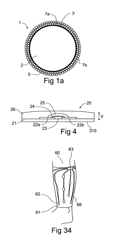
Referring to Figs la-2b, an elastomeric particle 1,
1', 1" according to the first aspect will now be
described. Such an elastomeric particle 1, 1', 1"
comprises an elastomeric body 2 and a conducting surface
layer 4a, 4b, 6. The conducting surface layer 4a, 4b, 6
may be formed by a plurality of conducting particles 7a,
7b, by deposition of a conducting material 6 (e.g. metal
or conducting polymer), or by modifying the conducting
properties of the surface of the elastomeric body 2 (e.g.
interpenetrating polymer networks with electrically
conducting polymer constituents). In the case of
conducting particles 7a, 7b, these may be adhered to the
elastomeric body 2 by a primer 3. One or more further
conductive layers 4b may be provided (as indicated in
Figs la and 2a), and preferably attached to the previous
layer 4a by a binder 5.
The size of the elastomeric particle 1, 1', 1" may
be in the range of 0.1-250 pm, more preferably in the
range of 1-10 pm. The elastomeric particle may have a
shape that is regular or irregular. As non-limiting
examples, the elastomeric particles may be rod-like,
ellipsoidal, spherical, platelets, granules, fibers,
porous shells, scaffolding etc. The elastomeric particles
may be hollow or solid. Generally, spherical elastomeric
particles may be produced by emulsion or suspension
CA 02676207 2009-07-22
WO 2008/089787 PCT/EP2007/000567
11
polymerization. Other shapes may be produced by e.g.
cryogenic pulverization or other breakdown processes,
such as grinding.
Another way of producing such elastomeric particles
is through seed polymerization, which is described in
e.g. JP-A 58-106554 and JP-A 63-191818. Yet another way
of producing such elastomeric particles is through
emulsion polymerization with additional conditions for
creating larger, crosslinked, elastomeric particles, such
as is described in US 6,914,100, JP-A 63-191805, JP-A 4-
323213 and JP-A 10-310603. The polymerization process can
be of any type, including radical, polyaddition or
polycondensation reactions.
The elastomeric particles may be cross-linked to
ensure suitable mechanical properties. It is noted that
the references above demonstrate creation of particles
that are crosslinked.
In a practical case, it may be convenient to
purchase elastomeric particles, which do not have a
conducting surface, in wet or dry form from various
suppliers, examples of which include Dow Corning, Shin
Etsu Chemical and Rohm and Haas for small particles, and
several chemical suppliers for larger particles.
Naturally, it is also possible to purchase pellets that
are to be pulverized or atomized. For example,
commercially available thermoplastic elastomer pellets
can be heated and spray dried to create smaller
particles, or alternatively cryogenically pulverized to
produce the same.
The elastomeric body 2 and/or the matrix 11, as will
be discussed below, may, as non-limiting examples
comprise silicone elastomers, polyurethanes,
polybutadiene (specifically high cis polybutadiene),
natural rubber, polyisoprene, ethylene-propylene-diene,
thermoplastic elastomers, segmented block copolymers,
etc. In particular, silicone elastomers have excellent
compression set, creep and temperature stability, and can
CA 02676207 2009-07-22
WO 2008/089787 PCT/EP2007/000567
12
be formulated with excellent fatigue properties, while
polyurethanes and polybutadienes can be formulated with
excellent dynamic properties (low hysteresis, high
resilience, long fatigue life, etc.). Specifically useful
are chain-extended PU elastomers with amide chain
extenders, with excellent temperature/frequency stability
of mechanical properties.
An example of a suitable material is provided in van
der Schuur, M, Noordover B, Gaymans RJ, 2006,
Polyurethane elastomers with amide chain extenders of
uniform length. Polymer, 47: 1091-1100.
There are also biomaterials with excellent
resilience, such as elastin and resilin, see Elvin CM,
Carr AG, Huson MG, Maxwell JM, Pearson RD, Vuocolo T,
Liyou NE, Wong DC, Merritt DJ, Dixon NE. 2005. Synthesis
and properties of crosslinked recombinant pro-resilin.
Nature. 437(7061): 999-1002.
In general, the elastomeric body 2 and the matrix 11
may be made from the same family of elastomer, with
different degrees of crosslinking or fillers to achieve
variations in hardness. One example of an easy to use
system is the three-component, variable mix ratio
polyurethane system from Crosslink Technology Inc.
(disclosed in US 2006/0058456), or their CLC system.
Examples of hardening filler materials include quartz,
silica, mica, carbon black, etc. These materials are
especially suitable for use as fillers in silicone
systems.
For the conducting layer 4a, 4b, 6, a range of
materials may be used, including metallic or metal oxide
conducting species, carbon and structures thereof,
conducting polymers etc. Combinations of these materials
may also be used.
In case alignment is desirable, the conducting layer
4a, 4b, may include materials from the known groups of
paramagnetic, super paramagnetic, or ferromagnetic
materials.
CA 02676207 2009-07-22
WO 2008/089787 PCT/EP2007/000567
13
In one embodiment, the particles 1, 1',1" may be
constructed by layer-by-layer self assembly (LbL-SA) or
layer-by-layer covalent self assembly (LbL-CSA)
approaches, which produces stronger interlayer bonding
than LbL-SA. In this case, the conductive materials (e.g.
metallic, metal-oxide, semiconductive or organic) forming
the conducting layers 4a, 4b will generally be
nanoparticulates 7a, 7b with useful examples being
nanoparticles of (including core shell particles) gold,
silver, platinum, palladium, copper, nickel, aluminum,
chromium etc. In particular, nanoparticles of gold are
easy to produce, and can be stored in a stable
configuration before the deposition process.
As one alternative, the conducting layer 4a, 4b, 6
may be provided by electroless deposition, which is a
well known method wherein a seed layer (catalyst), such
as palladium, is applied to the particles, and further
conducting material is deposited via reduction of a metal
salt onto the surface of the elastomeric particles. Such
a method is described in Mallory GO, Hajdu JB,
Electroless plating: fundamentals and applications,
American Electroplaters and Surface Finishers Society,
Florida, 1990. In such cases a primer 3 may be applied
prior to the deposition of the conducting layer.
The elastomeric particles may be somewhat swollen
during the application of the conducting layer 4a, 4b, 6,
regardless of which type of application technique is
selected so that when they are dried, the surface will
take on a microscopic texture, in addition the particles
will be more suitable for undergoing strain as their
surfaces will be wrinkled rather than smooth, since when
smooth and too thick, the conductive layers will
interfere with the mechanical properties of the particles
and can also crack, thereby losing their conductive
properties.
As another option, conducting polymers can be
electrochemically deposited on the surface of the
CA 02676207 2009-07-22
WO 2008/089787 PCT/EP2007/000567
14
elastomeric body 2. For example, a thin conducting
polymer layer can be deposited so as to produce an
inherently conducting layer over the elastomeric
particles using in situ oxidization. Such techniques are
described within US 5,240,644, US 6,899,829, Gregory RV,
Kimbrell WC, Kuhn HH, Synthetic Metals, 28 (1989), pg
823, and Hansen TS, West K, Hassager 0, Larsen NB,
Synthetic Metals, 156 (2006), pg 1203.
In the case of LbL-SA or LbL-CSA produced layers,
the conductivity of the layers is a combination of
quantum tunneling and physical contact between the
tightly packed conductive nanoparticles 7a, 7b arranged
within the layers over the surfaces of the elastomeric
particles 1, 1', 111. This tight knit structure minimally
affects the mechanical properties of the elastomeric
particle 1, 1', 111. This arrangement also allows the
elastomeric particles to maintain surface conductivity
even when the entire composite structure is strained.
The fluid environment in which the conductive
particles 7a, 7b are constructed must be compatible with
the elastomeric particles so that they are not damaged
during the assembly process and may be easily transferred
from one layering environment to the next without overly
demanding intermediate washing and/or drying steps. As
mentioned earlier, optimization of the fluid environment
can cause advantageous swelling of the elastomeric
particles during deposition of the conductive layers.
LbL-CSA or LbL-SA can also be used to form a
monolayer on the elastomeric particles, which would be a
seed layer, whereupon further conducting material is
deposited electrochemically, e.g. by electroless
deposition.
Examples of methods for depositing the conducting
nanoparticles 7a, 7b onto a surface by self assembly are
known from e.g. US2005/0064204, US 6,025,202, US
6,624,886, US 6,242,264, US 6,458,327, US 6,592,945.
CA 02676207 2009-07-22
WO 2008/089787 PCT/EP2007/000567
The process of building up multiple conducting
layers onto a surface is achieved through repetition of
deposition steps, as is disclosed in US2005/0064204 and
US 6,458,327.
5 Yet another option for forming the conducting layer
4a, 4b, 6 involves physical vapor deposition processes, a
variety of which are known, including vacuum evaporation,
sputtering and chemical vapor deposition. Deposition via
such methods is considered straight forward, except that
10 one may need to continually mix the elastomeric particles
to ensure adequate coverage with the thin conducting
material.
The thickness of the conducting layer 4a, 4b, 6
should be as thin as possible, so as not to add to the
15 overall mechanical stiffness of the final particle. This
is especially important when using methods that form
continuous layers onto the elastomeric particles.
Preferably, the conducting layer thickness may be
less than 10% of the diameter of the elastomeric
particle. More, the thickness may be less than 5%, less
than 1% or less than 0.1% of the diameter of the
elastomeric particle.
Expressed differently, the thickness may preferably
be less than 500 nm, more preferably less than 100 nm, or
less than 50 nm.
For a sensor type embodiment, the layers on the
elastomeric body 2 collectively should have an overall
quiescent sheet resistance of 0.1-100kS2/^, and more
preferably a sheet resistarice of 1-lOkS2/0.
For an electrical interconnect application, the
layers on the elastomeric body 2 should have an overall
quiescent sheet resistance of less than 1052/0, more
preferably less than 10/0, and most preferably less than
0. 1S2/^.
The primer 3 on the surface of the elastomeric body
2 is selected to initiate the deposition process onto the
elastomeric body surface, improve bonding between the
CA 02676207 2009-07-22
WO 2008/089787 PCT/EP2007/000567
16
elastomeric body and the first conducting layer, and/or
to improve bonding of the completed particles to the
matrix material. The primer 3 is generally chosen from
the known organosilanes and organosiloxanes with examples
provided below.
The organosilane compounds include compounds having
alkyl and alkoxide groups in one molecule such as
hexyltrimethoxysilane, octyltrimethoxysilane, cyclo-
pentyltrimethoxysilane and cyclohexyltrimethoxysilane;
organosilane compounds having vinyl and alkoxide groups
in one molecule such as vinyltrimethoxysilane; organo-
silane compounds having amino and alkoxide groups in one
molecule such as (N,N-dimethylaminopropyl)trimethoxy-
silane, (N,N-diethylaminopropyl) trimethoxysilane, amino-
propyltrimethoxysilane, N-(6-aminohexyl) aminopropyl-
trimethoxysilane, and (aminoethylaminomethyl)- phenethyl-
trimethoxysilane; compounds having ammonium and alkoxide
groups in one molecule such as N,N,N-trimethylammonio-
propyltrimethoxysilane; organosilane compounds having
heteroaromatic ring and alkoxide groups in one molecule
such as 2-(trimethoxysilylethyl)pyridine; organosilane
compounds having fluoroalkyl and alkoxide groups in one
molecule such as (3,3,3-trifluoropropyl)trimethoxysilane
and (decafluoro-1,1,2,2-tetrahydr- ooctyl) triethoxy-
silane; organosilane compounds having polyethyleneglycol
and alkoxide groups in one molecule such as N-(triethoxy-
silylpropyl)-O-po- lyethyleneoxide-urethane; organosilane
compounds having thiocyanate and alkoxide groups in one
molecule such as 3-thiocyanatepropyltriethoxysilan- e;
organosilane compounds having ether and alkoxide groups
in one molecule such as 3-methoxypropyltrimethoxysilane;
organosilane compounds having thiol and alkoxide groups
in one molecule such as 3-mercaptopropyltrimeth- oxy-
silane; organosilane compounds having halogen atom and
alkoxide groups in one molecule such as 3-iodopropyl-
trimethoxysilane and 3-bromo-propyltrimethoxysilane;
organosilane compounds having epoxy and alkoxide groups
CA 02676207 2009-07-22
WO 2008/089787 PCT/EP2007/000567
17
in one molecule such as 5,5-epoxyhexyl-triethoxysilane;
organosilane compounds having sulfide and alkoxide groups
in one molecule such as bis[3-(triethoxysilyl)-
propyl]tetrasulfide; organosilane compounds having
hydroxyl, amino and alkoxide groups such as bis(2-
hydroxyethyl)-3-amino-propyltriethoxysilane; organosilane
compounds having an amino group and groups derived by
hydrolysis of alkoxide groups in one molecule such as
aminopropylsilane triol; organosilane compounds having
alkyl group and chlorine atoms in one molecule such as
octyltrichlorosilane, cyclotetramethylenedi-chlorosilane,
(cyclohexylmethyl))trichlorosilane,cyclohexyl-trichlo-
rosilane, and tert-butyltrichlorosilane; organosilane
compounds having fluoroalkyl group and chlorine atoms in
one molecule such as (decafluoro-1,1,2,2-tetr- ahydro-
octyl)tri-chlorosilane and (3,3,3-trifluoropropyl)tri-
chlorosilane; organosilane compounds having heteroaro-
matic ring and chlorine atoms in one molecule such as 2-
[2-(trichlorosilyl)-ethyl]pyridine; and organosilane
compounds having an aromatic ring and chlorine atoms in
one molecule such as phenethyltrichlorosilane. See e.g.
US 2005/0064204.
Organosiloxane compounts generally include alkoxy-
silanes such as methyltrimethoxysilane, vinyltrimethoxy-
silane, 3-glycidoxypropyltrimethoxysilane, 3-methacryl-
oxypropyltrimethoxysilane, dimethyldimethoxysilane, tri-
methylmethoxysilane, trimethylethoxysilane, tetrameth-
oxysilane, and tetraethoxysilane; siloxane oligomers such
as silanol-endblocked dimethylsiloxane oligomers, sila-
nol-endblocked dimethylsiloxane/methylvinylsiloxane co-
oligomers, silanol-endblocked methylvinylsiloxane oligo-
mers, silanol-endblocked methylphenylsiloxane oligomers,
1,3,5,7-tetramethylcyclotetrasiloxane, and 1,3,5,7,9-
pentamethylcyclopentasiloxane; polyorganosiloxanes rang-
ing from low-viscosity liquids to gums, and including but
not limited to trimethylsiloxy-endblocked polydimethyl-
siloxanes, trimethylsiloxy-endblocked dimethylsilox-
CA 02676207 2009-07-22
WO 2008/089787 PCT/EP2007/000567
18
ane/methylvinylsiloxane copolymers, trimethylsiloxy-
endblocked dimethylsiloxane/methylphenylsiloxane copoly-
mers, trimethylsiloxy-endblocked polymethylhydrogen-
siloxanes, trimethylsiloxy-endblocked dimethylsil-
oxane/methylhydrogensiloxane copolymers, silanol-
endblocked polydimethylsiloxanes, silanol-endblocked
dimethylsiloxane/methylvinylsiloxane copolymers, silanol-
endblocked dimethylsiloxane/methylphenylsiloxane copoly-
mers, silanol-endblocked polymethylhydrogensiloxanes,
silanol-endblocked dimethylsiloxane/methylhydrogen-
siloxane copolymers, dimethylvinylsiloxy-endblocked
polydimethylsiloxanes, dimethylvinylsiloxy-endblocked
dimethylsiloxane/methylvinylsiloxane copolymers,
dimethylvinylsiloxy-endblocked dimethylsiloxane/methyl-
phenylsiloxane copolymers, dimethylhydrogensiloxy-
endblocked polymethylhydrogensiloxanes, and dimethyl-
hydrogensiloxy-endblocked dimethylsiloxane/methyl-
hydrogensiloxane copolymers; and silicone resins,
including but not limited to resins composed of
R3SiO1/2 and SiO4/2 units, silicone resins
composed of the RSiO3/2 unit, resins composed of the
R2SiO2/2 and RSiO3/2 units, and resins
composed of the R2SiO2/2, RSiO3/2, and
SiO4/2 unit. See e.g. US 7,074,849.
Further organosilanes with functional groups
including: epoxy, amino, ketimino, vinyl, methacryloxy,
acryloxy, mercapto, polysulfido, isocyanato, styryl and
hydrolysable groups including chloro, methoxy, and ethoxy
functional groups. See Shin Etsu Chemical silane coupling
agent brochure for similar listings.
In practice, a particular agent is generally
selected based on consultation of the literature, and
simple adhesion trials. In general, the coupling agents
are selected such that the coupling agents have organic
functional groups that match the reactivity of the
polymer surface in question.
CA 02676207 2009-07-22
WO 2008/089787 PCT/EP2007/000567
19
Known examples include aminopropyltriethoxysilane or
mercaptopropyltrimethoxysilane (depends on the base
material being bonded to), as disclosed in US2005/0064204
or US 6,458,327 for glass substrates, but groups can be
selected for the appropriate elastomer materials in
question.
There are also proprietary, commercially available
primers available from such companies as Dow Corning,
Shin Etsu Chemical, Nusil, among others.
The binding layer 51s used to bond together
subsequently deposited conducting layers. As examples of
binders for LbL-SA, materials containing two functional
groups such as hydroxyl groups, amino groups, carboxyl
groups, carboxylic acid anhydride groups, mercapto
groups, hydrosilicon groups and combinations thereof may
be used, as described in US2005/0064204. The selected
material should have at least one functional group that
can covalently or non-covalently bond to the desired
molecule, such as the nanoparticle or the elastomer.
Another name for these materials are ligands,
containing one or more amino groups, thiol groups, and
are chosen from the the group comprising mercaptoalkyl-
silanes, aminoalkylsilanes, dimercaptoalkanes, diamino-
alkanes, hydroxy-alkanes, carboxy-alkanes, dihydroxy-
alkanes, and dicarboxyalkanes, as disclosed in US6458327.
As an example for polyurethane/gold nanocomposites,
mercaptoethanol may be used as the binding agent.
As an example for a polysiloxane/silver
nanocomposite, polysiloxane may be used as the binding
agent. Specifically, poly(dimethyl-co.methylhydrido-co-3-
cyanopropryl,methyl)siloxane. The same polysiloxane as
used for the elastomeric materials of the composite may
be used directly as the binder (without primer), so as to
reduce the overall number of materials in the composite.
As an example for building up multiple gold
nanoparticle layers, 2-mercaptoethanol or 2-
mercaptoethylamine may be used, see US2005/0064204.
CA 02676207 2009-07-22
WO 2008/089787 PCT/EP2007/000567
Another example for building up multiple layers of
gold nanoparticles with dodecylamine stabilizing ligands
would be mercaptoalkylsilanes, aminoalkylsilanes,
dimercaptoalkanes, diaminoalkanes, or polyfunctionalized
5 polymers, as disclosed in US 6,458,327.
Referring to Figs 4-6b, the above described
elastomeric particles having a conducting surface may be
used to provide a pressure sensor element.
Fig. 4 schematically illustrates a first embodiment
10 of a pressure sensor element 20. The drawing is
magnified, and the vertical direction V is greatly
exaggerated. The measurement side is indicated by
reference numeral 310. The sensor element 20 is based on
a substrate 21, upon which a pair of electrodes 22a, 22b
15 are arranged. The electrodes may, but do not need to, be
co-planar. Electrodes 22a, 22b may be provided by
patterning a conducting material onto the substrate/first
elastomeric portion in any known manner. A first non-
conducting elastomeric portion 23 is arranged between the
20 electrodes. The first elastomeric portion 23 may cover
opposing edge portions of the electrodes 22a, 22b and it
may have a maximum thickness which is larger than that of
the electrodes. The thickness of the first elastomeric
portion 23 may taper or otherwise diminish towards its
edges.
On the first elastomeric portion 23, one or more
conducting layers 24 may be arranged. Such conducting
layers may comprise elastomeric particles as described
above, which are arranged in a matrix comprising a primer
and/or a binder as described above. The conducting layers
24 are in contact with the electrodes 22a, 22b. In
particular, a primer 3, such as the ones mentioned above,
may be used between the first elastomeric portion 23 and
the first conducting layer 24, and a binder 5, such as
the ones mentioned above, may be used between the first
conducting layer 4a and further conducting layers 4b.
CA 02676207 2009-07-22
WO 2008/089787 PCT/EP2007/000567
21
A second non-conducting elastomeric portion 25 may
be arranged on top of the conducting layers 24, such that
the conducting layers 24 are enclosed by the first and
second elastomeric portions 23, 25 with only edge
portions of the conducting layers 24 being exposed to the
electrodes 22a, 22b. Another primer or binder may be used
between the conducting layers 24 and the second
elastomeric portion 25. The elastomeric portions 23, 25
may be formed from any material mentioned above with
respect to the elastomeric body 2.
The sensor element, including the elastomeric
portions 23, 25, the electrodes and the conducting layers
24 may be enclosed in an isolation coating 26, which may
be non-conducting. The isolation coating 26 may be made
from an elastomeric material and may optionally be
foamed.
In one embodiment, the elastomeric portions 23, 25
are made from elastomeric materials having different
modulus of elasticity. In another embodiment, the
elastomeric portions 23, 25 are made from elastomeric
materials having substantially the same modulus of
elasticity.
When the sensor element 20 is subjected to pressure
(typically compression in the vertical direction V), the
relative positions of the particles present in the
conducting layers 24 will change, thereby changing the
impedance of the sensor element, as measured over the
electrodes 22a, 22b.
The sensor element 20 may be produced according to
the following.
A substrate 21 with electrodes 22a, 22b is prepared
and possibly cleaned. Such a substrate may e.g. be a
fabric or a polymer film. A primer may be applied to the
surface where the first elastomer layer 23 is to be
deposited. A first elastomer layer 23 with a first hard-
ness is deposited. A primer layer, with a primer as
described above, may then be deposited. Conductive layers
CA 02676207 2009-07-22
WO 2008/089787 PCT/EP2007/000567
22
24 are deposited to bridge the electrodes 22a, 22b and to
extend out past the first elastomer 23. Binder layers 5
as described above may be arranged between the conductive
layers 24. Another primer may be used to coat the
conductive layers 24. A second elastomer layer 25 with a
second hardness is deposited. This second elastomer layer
25 can also function as a mechanical isolation layer.
Optionally, an isolation coating 26 is deposited, and
optionally foamed. This isolation coating 26 also may
function as a stress filtering layer to smooth out
contact stresses applied to the sensor element in the
vicinity of the first and second elastomer layers 24, 25.
Fig. 5 illustrates an alternative embodiment of a
sensor element 20', wherein the first elastomer 23' has
been dispensed on the substrate 21 prior to the forming
of the conducting layer 24 and the electrodes 22a', 22b'.
The conducting layers 24 and/or the electrodes 22a', 22b'
may be patterned, e.g. dispensed, printed or jetted, onto
the substrate and onto the first elastomer 23'.
Fig. 6a illustrates another alternative embodiment
of a sensor element 20", wherein the first elastomer
23" has been molded onto the substrate. Subsequently,
the conducting layers 24 have been formed, and thereafter
the electrodes 22a ", 22b " have been printed.
Referring to Fig. 6b, there is illustrated a detail
on how the conducting layer 24 may be formed. In one
embodiment, the conducting layer 24 comprises one, two or
more layers of the elastomeric particles 1, 1', 1"
described above with reference to Figs la-2b. The
conducting layer 24 according to this embodiment may be
produced by applying a primer 3 in a desired pattern
where the conducting layer 24 is to be formed.
Thereafter, conducting particles 1, 1', 1" are applied
so as to form a first conducting layer 4a. A binder 5 is
thereafter applied in a desired pattern, after which
further conducting particles 1, 1', 1" may be applied so
as to form a second conducting layer 4b. This method may
CA 02676207 2009-07-22
WO 2008/089787 PCT/EP2007/000567
23
be used to provide the conducting layer of any of the
embodiments illustrated in Figs 4-6b.
In another embodiment, the conducting layer 24 of
Figs 4-6b may be formed in the any of the manners
described with reference to the conducting surface of the
elastomeric particles 1, 1', 1" of Figs la-2b. Thus, the
conducting layer 24 may be formed using primer 3 and/or
binders 5 as described with reference to Figs la-2b to
provide one, two or more layers 4a, 4b of non-elastomeric
conducting particles 7a, 7b. The technology disclosed in
US 2005/0064204A1 may be used to provide the conducting
layer.
It is noted that alternatively, the conducting layer
24 may be formed by patterning a compound for forming the
composite material described below, possibly after
deposition of a primer.
Fig. 3 schematically illustrates a composite
material 10 comprising elastomeric particles 1, 1', 1"
as described above and a matrix material 11.
The above described elastomeric particles 1, 1', 1"
may thus be used to provide a composite material 10,
which in turn may be used for forming pressure sensor
elements. Such a composite material may be formed by
mixing the elastomeric particles with a matrix material
11, which may also be an elastomeric material.
In practice, the matrix material may be
substantially the same as that of the elastomeric body 2
of the particles, however with a different hardness or
modulus of elasticity. Examples of suitable matrix
materials are thus given above with reference to the
elastomeric particle 2.
By using a composite comprising soft elastomeric
particles 1, 1', 111, it is possible to better manage
strain related damage, quiescent electrical impedance and
strain sensitivity of the electrical impedance within the
composites by improving and managing stresses at
CA 02676207 2009-07-22
WO 2008/089787 PCT/EP2007/000567
24
interfaces between matrix and particles, and within the
matrix.
The composite material thus comprises soft particles
1, 1', 1'' (elastomeric in nature) of a first modulus of
elasticity, the surfaces of which are made conductive (as
described above), mixed with a binder material
(elastomeric in nature) of a second modulus of elasticity
into a composite structure. The composite material may
also contain coupling agents, compatibilizing agents and
other particulates etc. to fine tune the final composite
properties.
The coupling agents or compatibilizing agent may be
chosen from the known organosilanes and organosiloxanes
with examples mentioned above.
Interfacial stresses and strain related damage may
be minimized when the first and second moduli of
elasticity are chosen to be substantially equivalent to
each other. Such an arrangement produces a composite with
low mechanical hysteresis, and low impedance strain
sensitivity while further improving the cycle life of the
composite and improving linearity of the strain-impedance
relationship of the composite.
Finite quiescent impedance can be set during
fabrication via alignment, volumetric ratios of
constituents and fabrication conditions (solvents,
compression, temperature profile during curing, etc).
Pressure sensitivity may be determined primarily by
the equivalent modulus of elasticity, the strain-
impedance relationship of the composite, and the
structure of the sensor built from the composite
(geometry, field orientation, electrode placement, etc.).
Strain sensitivity can be increased in a controlled
manner by changing the ratio between the first and second
moduli of elasticity.
The soft elastomeric particles 1, 1', 1" can be
mixed randomly with a matrix-forming material (and other
CA 02676207 2009-07-22
WO 2008/089787 PCT/EP2007/000567
particles) or used in conjunction with preferential
alignment (see below).
Alignment, as will be further discussed below, can
be used to further affect strain sensitivity of the
5 electrical impedance of the composite.
The mechanical properties of the overall system are
primarily related to the mechanical properties of the
constituent components (particles, matrix, and the
difference between the two), the mix ratios, alignment
10 configurations, as well as the strength of the bonds
between the particles and the matrix.
The pressure sensitivity of the electrical impedance
is then a function of the strain sensitivity and the
mechanical properties of the composite.
15 A mixture or compound 10 (see Fig. 3) comprising
elastomeric particles 1, 1', 1" and matrix-forming
material 11 may be provided. The compound may be in the
form of a paste. The matrix-forming material may be
allowed to harden or set into any of the materials
20 mentioned above as being suitable for the elastomeric
body 2 or matrix 11, or similar/equivalent materials.
Such a compound may be e.g. printed or deposited in order
to provide sensor elements as illustrated in Figs 4-10
and then allowed to harden or set. Curing may be
25 facilitated in any way known to the skilled person, such
as by influence of radiation etc.
In the composite material arranged with generally
randomly distributed soft elastomeric particles, the
volume percent of coated particles into a matrix, for
randomly distributed particle systems, will generally be
in the range of 10-75% by volume. This is in line with
the volume percent of prior art sensory materials.
In cases of alignment, as described below, generally
the required volume percent of particles may be reduced
by a factor of 10 to 100. This will further benefit the
mechanical properties of the resulting composite as the
CA 02676207 2009-07-22
WO 2008/089787 PCT/EP2007/000567
26
reduced amount of interfaces will further reduce
mechanical hysteresis during use.
Referring to Figs 7-10, the description will now be
focused on sensor elements using a composite material as
described above.
Fig. 7 schematically illustrates a first embodiment
of a sensor element 30, wherein a substrate 31 is
provided with electrodes 32a, 32b. A conductive composite
33, such as the one described above, is then provided on
the substrate and in contact with the electrodes.
Optionally, an isolation coating 34, such as the ones
described with respect to Figs 4-6b, may be provided to
encapsulate the sensor element 30.
Fig. 8 schematically illustrates a second embodiment
of a sensor element 30', which is similar to the one of
Fig. 7, but provided with a second substrate 31a, with a
third electrode 32c. The second substrate is spaced from
the first substrate, and may be "floatingly" arranged in
the composite material 33. The second substrate 31a with
its associated electrode may be produced in the same way
as the first substrate 31. The third electrode 32c can be
used to facilitate preferential alignment within the
composite material 33 during fabrication, augment the
electrical impedance of the sensor element 30, provide
more suitable area within the composite material 33 where
impedance measurements can be taken, preferentially
spread applied stress over the composite material 33,
provide a means of measuring pressure gradients applied
to the sensor element 30, or electrically shield the
sensor element 30 from the surroundings.
Fig. 9 schematically illustrates a third embodiment
of a sensor element 3011, wherein a non-conducting
elastomeric portion 35 is provided between the electrodes
32a, 32b in a manner similar to that of Figs 4 or 5, e.g.
in order to reduce stress concentrations around the edges
of the electrodes, to control stresses in the composite
material 33', to separate the stress and field
CA 02676207 2009-07-22
WO 2008/089787 PCT/EP2007/000567
27
concentrations within the composite material 33' and/or
to facilitate preferential alignment in the composite
material 33' during fabrication of the sensor element
30". The elastomeric portion 35 may be further foamed to
alter the hardness and the Poisson's ratio of this
portion of the sensor element 30". This provides a
further means of controlling pressure sensitivity of the
sensor element 30"
Furthermore, in Fig. 9, the portion of the composite
material 33' extending between the electrodes 32a, 32b
may be structured, e.g. made narrower, so as to further
control sensitivity of the electrical impedance of the
composite material 33' to applied pressure, and locally
alter the mechanical properties of the composite material
33'.
In the embodiment of Fig. 9, a third electrode with
substrate as described with reference to Fig. 8 may be
included.
Fig. 10 schematically illustrates a fourth embodi-
ment of a sensor element 301", which is arranged in a
through hole 36 in the substrate 31. Such a substrate may
e.g. be a fabric or a polymer film. The composite
material 33" may be symmetrically arranged in relation
to the substrate 31. Electrodes 32a', 32b' may be
provided by a wire embedded in or arranged on the
substrate 31, or as a conductive yarn provided in a
fabric. Electrodes 32a', 32b' may also be provided by
patterning a conducting material onto the substrate in
any known manner. In the latter case, the wires leading
to the electrodes may be provided with an isolating
coating, which is removed to expose the conducting part
to thereby provide the electrodes 32a', 32b'. Such
removal may be achieved by e.g. etching, solvent,
mechanical ablation etc. This embodiment is particularly
suitable for creating very thin sensor systems.
CA 02676207 2009-07-22
WO 2008/089787 PCT/EP2007/000567
28
In this embodiment, isolation coatings 34a, 34b may
be provided on both sides of the substrate 31, such as to
encapsulate the sensor element.
In the embodiment of Fig. 10, the third electrode
with or without associated substrate, as described with
respect to Fig. 8 may be provided.
In the embodiments of Figs 7-10, the composite
material may optionally be foamed, in a per se known
manner.
A production process for providing the sensor
element of Figs 7-10 may include providing a suitable
substrate material; providing electrodes on the
substrate, e.g. by a patterning process; depositing a
mixture for forming the composite material (including
elastomeric particles and matrix material); optionally
providing a field application fixture and apply the
requisite fields (AC, DC, ramp-up, hold, ramp-down) for
alignment; curing the matrix material (e.g. by
application of UV light, heating etc.); removing any
alignment field; optionally post curing the matrix
material; and removing any remaining alignment field, if
not removed early in the curing process. Optionally,
conductive bridges between sensors and external
electronics may be provided, e.g. by printing,
lithographic patterning, etc.
It is recognized that there are many electrode and
magnet arrangements for alignment as well as mechanical
layouts that may be optimized for this type of sensor.
It is noted that for the embodiments described with
reference to Figs 4-10, the electrodes may be a conduc-
ting compound, metal or conducting organic material.
Application methods include PVD, CVD, electrochemical
methods, inkjetting, printing etc., followed by any
necessary sintering or drying steps.
Substrate materials for providing the substrate of
the embodiments disclosed with reference to Figs 4-10
include films (preferably biaxially oriented polymer
CA 02676207 2009-07-22
WO 2008/089787 PCT/EP2007/000567
29
films including polyethylene terephthalate, polyethylene
naphthalate, but also polymer films including
polycarbonate, polyamide, polyimide, nylon,
polyethersulfone, aromatic fluorine-containing
polyarylates, etc.), fabrics (both woven and nonwoven),
felts, apertured films and foams (such as PU foam).
As indicated above, in the embodiments illustrated
with reference to Figs 4-10, it is possible, and
sometimes desirable, to preferentially align the
elastomeric particles of the composite between the
electrodes during fabrication. Motives for so doing
include reducing the volume fraction of particulate in
the conducting elastomer composite. This process may
improve two important aspects of the sensor properties:
(i) hysteresis is improved due to the fact that fewer
interfaces are present to form stress concentrations
throughout the composite material, and (ii) the
elastomeric particles may be localized only to the
regions of the sensor where they are needed. Furthermore,
alignment allows for the monitoring and control of the
quiescent impedance of the sensors during fabrication and
aging (post fabrication), thereby increasing yield and
more tightly controlling the final properties of the
sensors.
In the same regard, alignment can allow individual
sensors within a cluster or garment to be adjusted so as
to be similar to each other within each final product. It
may also allow flexibility in terms of calibrating some
sensors within a garment to behave with different
quiescent impedance than others for various applications.
For example, it may be possible to provide a
composite, where all sensor elements are tuned to have a
quiescent impedance of l0kohm under application-like test
conditions.
As another example, some sensor elements may be
tuned to behave more like switches with high sensitivity
(for determining garment state e.g. donned, removed),
CA 02676207 2009-07-22
WO 2008/089787 PCT/EP2007/000567
while others maintain lower sensitivity (for making
accurate measurements during treatments).
The alignment discussed above may most easily be
performed using B-fields, E-Fields, or combinations
5 thereof during the fabrication of the sensor element.
Of course, to use B-fields, the particles should
have a suitably high magnetic permeability, such that
they can move within the composite upon the application
of an external field.
10 E-field systems will work for any particle types. It
may be preferable that an AC field is used and that the
application frequency is sufficiently high, such that the
field does not collapse (breakdown) if a solid chain of
particles is formed between the electrodes. Field
15 collapse is not good in general, as it prevents
surrounding particles from forming chains within the
composite of the sensor, i.e. without control of E-field
collapse, one gets only a single connection between
electrodes that is very fragile in practice.
20 For E-field systems, it is also possible to use a
soft barrier layer around the elastomeric particles, such
that the breakdown effect will not be as dramatic, i.e.
as particles come together into chains, the impedance
drops more gradually and therefore breakdown of the field
25 does not occur suddenly as can happen with purely
conducting fillers. Such a barrier layer can be formed by
a primer layer applied to the external surface of the
particles before mixing them with the matrix. For some
matrix material, and conducting layer combinations, such
30 a barrier layer is formed naturally such as is the case
for silicone matrices and nickel conducting layers.
For both types of fields, in situ stirring is
possible using rotating fields. This can be useful for
slowly guiding particles into position without creating
strong single chains and will generally result in more
particles forming along the desired pathway than with.
CA 02676207 2009-07-22
WO 2008/089787 PCT/EP2007/000567
31
only one field element applied between the requisite
electrodes.
The electrodes applying the field may be the sensor
electrodes themselves, but they may also be separate
electrodes provided in a manufacturing fixture or mold.
Combination of fields may be useful as the presence
of one field can significantly reduce the requirements
for the other field. For example, permanent magnets may
establish a B-field in the vicinity of the sensor element
electrodes, whereby particles begin movement towards the
electrodes due to the presence of the B-field. Then an E-
field applied at the electrodes may be used to finish the
alignment process with much lower voltage requirements,
e.g. dropping the voltage requirement by a factor of 10-
100 times.
Passive structures can also be printed onto the
sensor to guide the particle traces and further assist
with the alignment process. For example, a printed
elastomer layer, between electrodes, with different
hardness than the conducting elastomer blend, may be
printed such that when an E-field is applied to the
electrodes, particles align primarily from the centers of
the electrodes rather than the edges. This prevents
collocation of field concentrations between the test E-
field and stress fields in the sensor during operation,
thus improving repeatability within the sensor element.
An example of such an elastomer is shown in Figure 9.
Referring to Figs 11-22, another type of sensor
element 40 will now be described. This type of sensor
element may be used on its own or in combination with the
sensor elements 20, 30 described above.
The sensor element 40, 40' , 40" , 40"' , 401", 40 ,
40vI, 40vij and associated embodiments as described in the
following are advantageous as sensor elements in that
they have improved mechanical response and aging
characteristics, immunity to EMI, and the ability to be
used for inline calibration of compression systems.
CA 02676207 2009-07-22
WO 2008/089787 PCT/EP2007/000567
32
This type of sensor can be most basically be
characterized as an array of contact switches with
pressure defined switching levels.
Referring to Figs 11-16, the sensor element 40
comprises a first substrate 41 with patterned metallic
electrodes 43a, 43b, 42a-1, 42a-2, 42a-3, 42a-4, 42a-5,
42a-6, a spacer 45, and a second substrate 47 with
patterned metallic electrodes 42b, wherein the first
electrodes comprises an array of electrode elements 42a-
1, 42a-2, 42a-3, 42a-4, 42a-5, 42a-6, which are separated
from each other by a spacing S. A resistive element 44
forming a conduction path is arranged on the first
substrate 41, such that the electrode elements 42a-1,
42a-2, 42a-3, 42a-4, 42a-5, 42a-6 contact the resistive
element 44 at different portions along the conduction
path. Connector electrodes 43a, 43b are provided at
spaced apart portions of the resistive element 44,
typically at end portions of the conduction path.
The second substrate 47 is arranged substantially
parallel with the first substrate 41, and spaced from the
first substrate 41 by the spacer 45. On the second
substrate 47, there is a second electrode 42b, which is
spaced from and faces the first electrode 42a. The second
electrode 42b may be formed as a continuous sheet, the
extent of which substantially coincides with an effective
overall extent of the first electrode 42a-1, 42a-2, 42a-
3, 42a-4, 42a-5, 42a-6.
The spacer 45 forms a cavity 48 between the first
and second substrates 41, 47. This cavity may be vented,
so as to equalize air pressure inside and outside the
sensor element.
The cavity 48 need not be rectangular or circular in
shape. It can be formed into many shapes including,
rectangles, circles, ellipses, dumb-bell like shapes,
polygons, and perturbations thereof. Circles are useful
for minimizing stresses at the edges of the cavity 48,
CA 02676207 2009-07-22
WO 2008/089787 PCT/EP2007/000567
33
while rectangles are easily patterned by standard
manufacturing processes.
In one embodiment, the resistive element is arranged
outside or adjacent the cavity. Hence, the resistive
element need not contact the movable parts of the
electrode(s), which decreases its sensitivity to wear.
When the sensor element 40 is subjected to pressure,
the first and second substrates 41, 47, and thereby also
the first and second electrodes 42a-1, 42a-2, 42a-3, 42a-
4, 42a-5, 42a-6, 42b, are pressed towards each other, so
that an area of contact between the first and second
electrodes 42a-1, 42a-2, 42a-3, 42a-4, 42a-5, 42a-6, 42b
is provided. The area of contact will increase
continuously, as more pressure is applied. As the area of
contact increases, more and more of the first electrode
elements 42a-1, 42a-2, 42a-3, 42a-4, 42a-5, 42a-6 will
become "short circuited" by the second electrode 42b,
thereby providing a shunt path past the conduction path
provided by the resistive element 44. Hence, the
impedance of the sensor element 40 will decrease stepwise
as a function of the applied pressure. This is
illustrated in Fig. 17, which illustrates a behavior of
an embodiment with a number of first electrode elements
42a-1, 42a-2, 42a-3, 42a-4, 42a-5, 42a-6 that
successively contact the second electrode 42b, so as to
shunt the resistive element 44 to decrease the overall
impedance of the sensor 40.
The elements of the first electrode 42a-1, 42a-2,
42a-3, 42a-4, 42a-5, 42a-6 are patterned such that they
are shunted at the appropriate pressure levels. For
example, for an application which requires that the
patient is subjected to 10 mmHg 3 mmHg for some time
period, followed by 50 mmHg 5 mmHg, and the overall
pressure applied should not exceed 70 mmHg, the traces
could be arranged such that shunting occurs at 7 mmHg, 13
mmHg, 45 mmHg, 55 mmHg, and 70 mmHg. Another alternative
CA 02676207 2009-07-22
WO 2008/089787 PCT/EP2007/000567
34
would be that the traces are arranged such that shunting
occurs at 10 mmHg, 50 mmHg and 70 mmHg.
Hence, points of discontinuity between the pressure
and impedance relationship of the pressure sensor element
40 may be determined by the number of first electrode
elements 42a-1, 42a-2, 42a-3, 42a-4, 42a-5, 42a-6, their
size and relative position with respect to each other and
within the cavity 48, as well as the thickness of the
spacer 45, the mechanical properties of the first and
second substrates 41, 47 and the overall dimensions of
the cavity 48. In embodiments with a large number of
first electrode elements, the sensor element 40 will more
closely approximate an analog relationship between
impedance of the conduction path and the applied
pressure.
The resistive element 44 may be formed as a
patterned resistive trace (e.g. by means of printing,
vacuum evaporation, thermal transfer printing etc.) or as
an array of discrete elements. This resistive element may
be arranged outside the flexible part of the sensor
element 40. The resistive element 44 may most easily be
provided by printing using traditional resistive inks or
pastes. The resistive element 44 will generally be
encapsulated or covered by the spacer layer 45, such that
it is not subjected to significant pressure application
during typical operations, and thus the resistance of the
resistive element 44 will not vary significantly during
operation. Stiff, well characterized inks and pastes can
be used for the resistive element 44 to ensure that
suitable properties are maintained during use. In
addition, due to the discontinuous nature of the pressure
- impedance relationship for such a sensor, moderate
variations in the resistance of the resistive element 44
can be easily tolerated over the life of the sensor
element 40 without degradation of performance.
The manner in which the elements of the first
electrode 42a-1, 42a-2, 42a-3, 42a-4, 42a-5, 42a-6 are
CA 02676207 2009-07-22
WO 2008/089787 PCT/EP2007/000567
connected to the resistive element 44 can be a serial
connection, parallel or any combination thereof. Full
advantage of connection possibilities can be used to
optimally shape the pressure - impedance relationship of
5 the sensor element 40.
In addition, in the case where the resistive element
44 is made from several individual resistor elements,
these need not be equal to one another. For example, in
the above case, the resistance change for the shunt at 7
10 mmHg may be significantly smaller than that at 13 mmHg,
so as to most clearly define the output resistance around
the desired operating point. This may be useful when the
device is operated in very hostile electromagnetic
environments.
15 The sensor element 40, 40' , 40" , 40"' , 401v, 40v,
40vi, 40vii may be built from structurally sound materials,
such as biaxially oriented films, and metallic, carbon,
or metal oxide layers, which are thin and deposited from
pure materials (no particulate based inks etc. are
20 needed). The spacer may be attached directly to the
adjacent membranes without pressure sensitive adhesives
or other creep prone materials, e.g. by welding. This
ensures that the creep and other undesirable mechanical
effects are minimized within the flexible components of
25 the sensor element 40, 40' , 40" , 40111, 40iv, 40v, 40vi,
40vir.
The substrates 41, 47 may be in the form of
membranes of biaxially oriented films of engineering
polymers. Primarily, biaxially oriented polymer films,
30 such as polyethylene terephthalate, polyethylene
naphthalate and also polymer films including
polycarbonate, polyamide, polyimide, nylon,
polyethersulfone, aromatic fluorine-containing
polyarylates may be used. Membrane thickness is generally
35 less than 25 micron, preferably less than 10 micron, most
preferably 2-5 micron.
CA 02676207 2009-07-22
WO 2008/089787 PCT/EP2007/000567
36
Electrodes 42a-1, 42a-2, 42a-3, 42a-4, 42a-5, 42a-6,
42b, 43a, 43b may be formed by patterning onto the
substrate 41, 47 using physical or chemical vapor
deposition techniques. Typical conducting materials for
electrodes may be silver, gold, copper, aluminum,
titanium, chromium, nickel, etc. Alternatively,
electrodes may be provided by conductive films and may be
patterned using electroless deposition, electrochemical
deposition, LbL self assembly and other techniques known
in the art. It may be advantageous if the electrodes are
at least partially composed of multiple layers. A base
layer may be a compatibilizing layer, such as Cr, Ti,
NiCr to improve adhesion to the substrate 41, 47, a
second layer may be a highly conducting layer, and an
upper layer may be a protective layer.
It is possible to deposit a thin overcoating layer
301, to protect one or both of the electrodes from damage
due to repeated contact during operation. One example of
a suitable material for an overcoating layer would be
graphite, another would be chrome or chrome alloys. Such
top layers can be applied via PVD, CVD, electrochemical
or self assembled means.
The electrodes may preferably be patterned using
lithographic techniques to ensure that smooth lines are
patterned and finely spaced onto the substrates 41, 47.
It is preferable that the thickness of the
electrodes are maintained at less than 1 um, more
preferably less than 500 nm, so that the influence of the
mechanical properties of electrodes on the performance of
the sensor element 40, 40' , 40" , 401 1 ' , 401v, 40v, 40vi,
40vij is minimized.
Alternatively, if the electrodes are being placed
onto a substrate that does not flex significantly, a thin
film type ink can be used to provide the electrode. Such
films can be patterned using printing techniques such as
inkjet, pad, and offset printing, among others.
CA 02676207 2009-07-22
WO 2008/089787 PCT/EP2007/000567
37
Nanoparticulate conducting inks can be employed for
this layer. In order to improve the mechanical robustness
of the ink, it may be sintered after deposition. Low
temperature sintering of the nano-ink is only suitable
when depositing conductors onto films with high
temperature resistance, such as fluorene polyarylates,
polycarbonate, polyethersulfone, polyimide or heat
stabilized biaxially oriented films of PET or PEN.
Another suitable alternative, which is known per se,
may be to apply an LbL self assembled wear resistant
layer to the electrodes.
The spacer 45 should be selected so as to present
low creep and good bonds to the substrates 41, 47. For
example, it can be a biaxially oriented film, that is to
be laminated together with the adjacent substrates. Such
lamination should be performed using the thinnest possi-
ble adhesive layers (preferably thermosetting adhesives),
as the presence of adhesive may adversely affect creep.
Many films are commercially available with suitable
adhesive surface layers.
The spacer 45 can also be provided in the form of a
patterned printed layer of a curable epoxy resin, a high
performance polyurethane resin or alternative, that may
be further cured and used both as the spacer 45 and to
bond together adjacent substrates 41, 47. In this case,
care must be given to creeping of the spacer 45 during
use, and reinforced resin systems may be used for the
spacer 45 to further improve its mechanical properties.
The spacer may include both an extension of the
cavity 48 within the sensor (air reservoir) as well as a
vent 46 or series of vents to equalize pressures between
the sensory element and the ambient environment.
External connections to the sensor element 40 may be
provided in the form of printed silver traces or the
like. Alternatively, it may be advantageous to use the
electrode patterning technique everywhere, i.e. both for
the electrodes and for the external connections. The
CA 02676207 2009-07-22
WO 2008/089787 PCT/EP2007/000567
38
trace thickness away from the sensing area may be
increased by masking the sensor regions, and using an
electrochemical technique to add conductor thickness to
the traces leading from the sensor elements to the
electronics.
Reel-to-reel techniques are suitable for mass
production of the sensor element 40, 40', 40" , 40" ',
401v. 40v, 40vI, 40vII
An isolation material 49a, 49b may be provided in
the form of e.g. a foamed polymer, which may generally be
very soft, with small pores. The isolation material 49a,
49b should be significantly softer than the substrate
materials 41, 47, so as not to interfere with the
function of the sensor element 40, 40', 40", 40"' , 401v,
40v, 40vI, 40vII, but so as to also provide a thin, but
smooth interface with the surrounding surfaces.
Fig. 18 illustrates the behavior of an embodiment
wherein the electrodes 42a-1, 42a-2, 42a-3, 42a-4, 42a-5,
42a-6, 42b have been made from a poorly conducting
material, i.e. resistive material. Such resistive
materials may be provided from e.g. nickel-chrome,
tantalum, tantalum-nitride, chromium, titanium, silicon-
chromium, cermet, carbon. Such materials can be deposited
by evaporation, sputtering, cvd, etc.
By using such materials for the electrodes, it is
possible to create sheet resistance on the electrodes
42a-1, 42a-2, 42a-3, 42a-4, 42a-5, 42a-6, 42b in a range
similar to that of the resistive element 44.
In addition, thin film inks can also be used, as
they are sufficiently thin so as to not adversely affect
the mechanical properties of the flexible substrate 41,
47 materials. Generally, silver loaded inks are satis-
factory for this purpose. Other inks based on particles
of the above materials can also be used to achieve parti-
cular sheet resistance or improve mechanical strength of
the contact interface between membranes. The equivalent
sheet resistance of the electrode 42b can also be
CA 02676207 2009-07-22
WO 2008/089787 PCT/EP2007/000567
39
adjusted by patterning of the deposited electrode
materials.
Furthermore, the sheet resistance can be modified by
using nanoparticulate layered thin films as producible
using LbL-CSA, or LbL-SA.
Figs 19a-19c illustrate alternative embodiments of
the resistive element 44 and the connectors 43a, 43b.
Such embodiments are useful for tailoring the pressure -
impedance response of the sensor element 40, 40', 40",
401 1' , 401", 40v, 40 1, 40"11
.
Specifically, they are useful for controlling the
height of the various discontinuities shown in Figs. 17
and 18.
In Fig. 19a, the resistive element 44 is formed as a
substantially rectangular elongate structure, while the
connectors 43a', 43b' are arranged at respective ends of
the resistive element.
In Fig. 19b, the resistive element 44' presents a
varying width and/or thickness, being elongate and
concave, while the connectors 43a', 43b' are arranged at
respective ends of the resistive element. More generally
the resistive element 44' is shaped in a continuous
fashion without discontinuities in width along the
conducting path.
In Fig 19c, the resistive element 44" presents a
varying width and/or thickness, including broader end
portions and a broader middle portion, spaced apart by
respective narrower intermediate portions. More
generally, the width of the resistive element 44" may be
varied along the conductive path in a step wise fashion
to tailor the step height of discontinuities in the
pressure - impedance response of the sensor element
40" '. This form of adjustment of the resistive element
44" is a simple way of tailoring the sensor response to
distinguish critical pressure transitions when used in
hostile environments with significant EMI.
CA 02676207 2009-07-22
WO 2008/089787 PCT/EP2007/000567
Fig. 20a and 20b illustrates an embodiment of an
electrode configuration, wherein the increase in contact
area between the first electrode 42a-1, 42a-2 and the
second electrode 42b' alters the slope of the pressure -
5 impedance relationship of the sensor element 40i" around
the point Pl. Such an embodiment may be provided by using
poorly conducting electrodes. The effect may be achieved
by the first electrode elements 42a-1, 42a-2 being of a
varying width and/or a reduction in gap spacing between
10 two elements at some point along their length. This may
be useful for enhancing the sensitivity of the sensor to
pressure in a particular range. This can be especially
useful for adjusting the sensitivity of the sensor
element 40, 40', 40", 40111, 401", 40", 40 1, 40 11 at
15 higher pressure levels where it is very important to
remain below a maximum pressure limit while performing a
therapy.
Fig. 20b illustrates the behavior such an
embodiment: the slope of the pressure-impedance curve is
20 discontinuous at the point P1.
Figs 21a-21b illustrates another embodiment of an
electrode configuration, wherein the increase in contact
area between the first electrode element 42a-1, 42a-2,
42a-3 and the second electrode 42b " alters the slope of
25 the pressure - impedance relationship of the sensor
element 40" around point P2 while also introducing a
discontinuity around P2. In this embodiment, the lengths
of the elements 42a-1, 42a-2, 42a-3 do not extend across
the entire sensor area. Then, as the contact region
30 between the first and second electrodes 42a, 42b expands
with increasing applied pressure, more or less elements
will come into contact.
This will cause both a change in sensitivity similar
to the example of Figs 20a-20b, but will also produce a
35 jump discontinuity at the point P2 of contact with the
shorter element. This point can then be more easily used
as a pressure calibration point for the sensory array.
CA 02676207 2009-07-22
WO 2008/089787 PCT/EP2007/000567
41
Fig. 22a illustrates another embodiment of a sensor
element 40vi, wherein the resistive element 44" ',
providing the conductive path, is substantially circular,
and the "fingers" of the first electrode 42a-1, 42a-2,
42a-3, 42a-4, 42a-5, 42a-6, 42a-7, 42a-8 extend
substantially radially from the resistive element and
towards the center of the sensor element 40vi.
Connectors 43a " and 43b " are arranged at the
respective ends of the resistive element 44" '. The
elements of the first electrode 42a-1, 42a-2, 42a-3, 42a-
4, 42a-5, 42a-6, 42a-7, 42a-8 may present different
lengths, and the spacer 45a may be provided as a ring
around the sensor element 40vii. The second electrode 42b'
is spaced from the first electrode element 42a-1, 42a-2,
42a-3, 42a-4, 42a-5, 42a-6, 42a-7, 42a-8 in a manner
similar to that described with respect to Figs 11-16.
Sensor element 40vi is advantageous in that its
circular form allows for uniform stress at the spacer
45a, thereby providing a sensor element 40vI with improved
fatigue life.
Fig. 22b illustrates another embodiment of a sensor
element 40vij, comprising a pair of resistive elements
44a, 44b, each forming a respective conduction path. The
resistive elements 44a, 44b have respective connectors
43a "', 43b "', which may also interconnect the resistive
elements 44a, 44b, as illustrated, such that they are
connected in parallel. A number of first electrode
elements 42a are connected to the first resistive element
44a at a respective position along the conduction path of
the first resistive element 44a. Similarly, a number of
first electrode elements 42a are connected to the second
resistive element 44b at a respective position along the
conduction path of the second resistive element 44b.
Thus, first electrode elements 42a extend from the
respective resistive element 44a, 44b and into an active
area of the sensor, which may generally coincide with the
cavity of the sensor element 40vii. The cavity is defined
CA 02676207 2009-07-22
WO 2008/089787 PCT/EP2007/000567
42
by the patterned shape of the spacer 45a. In this
example, the cavity is defined by a spacer 45a comprising
a circular hole as shown in Fig. 22b.
Extra ventilation and air reservoirs are not shown
in Fig. 22b but may be added as previously discussed.
The first electrode elements of this embodiment may,
but do not need to, present mutually different lengths.
This embodiment increases the maximum possible
switch levels available from the sensor without
significantly increasing the size of the sensor. It also
adds flexibility in terms of optimizing the pressure-
impedance response of the sensor element.
In Figs 11-13, 16 and 22a-22b, the characteristic
length L, characteristic width W and overall sensor
thickness T (including isolating layers 49a, 49b) are
indicated. Also, in Fig. 16, there is indicated the
sensor body thickness S.
Generally, the sensor body thickness R should be
very small, preferably less than 50 pm, more preferably
less than 25 pm or less than 20 pm. The overall sensor
thickness T is preferably less than 1.5 mm, more
preferably less than 1 mm, more preferably less than 0.5
mm or 0.2 mm. The ratio between L and/or W and T may be
about 1.
Referring to Figs 4-10, the same ratios between
sensory region length/width and thickness, and between
sensor body thickness and isolation layer thickness,
apply.
It is not a requirement that the electrode elements
be arranged as lines in an array (as shown in Figs 11-14,
19a-19c, or 22b), or as radial spokes (as shown in Fig.
22a). It is quite possible to attain useful sensors by
providing sensor elements comprising first electrode
elements with rectangular, linear, elliptical, circular,
spiral, or exotic shapes and perturbations thereof.
CA 02676207 2009-07-22
WO 2008/089787 PCT/EP2007/000567
43
It is also possible to mix and match differently
shaped electrode elements and cavities to suit the
particular needs of a given application.
One example that can be particularly useful is a
combination of rectangular-shaped electrode elements in a
grid-like formation (easily patterned) with a circular-
shaped cavity (minimized edge stress). Such a circular-
shaped cavity can be easily provided by a perforated film
spacer 45. An example of this configuration is
exemplified by Fig. 22b.
The description will now focus on schemes for
connecting and arranging the above discussed sensor
elements. In particular, these schemes address the
problem of variations in pressure within the measuring
device. Contact pressures between surfaces can vary
widely, and often in a periodic manner, over short
distances between two surfaces in contact. Such
variations occur due to the random nature of contact
mechanics and the texture of the materials at the contact
interface. These variations are further exaggerated when
light pressures are applied between textured surfaces
(such as fabric layers pressed against a body for
example). In these cases, pressure is primarily
transmitted through apexes at the interface between the
surfaces during initial contact and tends to settle out
as the interface materials creep under continued contact
pressure.
If a sensor system is to adequately measure the
contact pressures between two surfaces, it should
preferably be able to cope with these unavoidable aspects
of contact mechanics.
The geometric issues of measuring representative
stresses between two surfaces can be remedied by using
sufficiently thick isolation layers between the sensor
elements and the surfaces in question to alleviate
pressure variations in the vicinity of the pressure
sensor. This task is not easy to accomplish when
CA 02676207 2009-07-22
WO 2008/089787 PCT/EP2007/000567
44
measuring pressures applied to body parts as overly thick
isolation layers make the device uncomfortable for the
patient, and curvature makes use of such layers
impractical. Instead, the sensor elements should be made
sufficiently small such that a thin isolation layer is
suitable for averaging out the microscopic stress
variations present in the immediate vicinity of a single
sensor element. Unfortunately, the randomness of contact
mechanics prevents a lone sensor from recovering the
overall characteristics of stress between the contact
surfaces.
One way of handling this problem is to provide a
large number of miniature sensors, and to analyze the
signals from each of the sensors in order to provide a
useful result, which may be an average pressure estimate
over the area of the sensor array. However, this would
require a large number of sensors to be individually
connected to a processing unit. The processing unit would
also need sufficient processing power to perform the
analysis from such a large number of sensors, and under
realistic operating conditions with associated cost,
power, and time constraints.
This task is further complicated in that pressure
sensor elements are nonlinear by nature. Therefore, the
processing unit would require an array of individually
calibrated lookup-tables, or configurable algorithms to
convert sensor singles into "pressure estimates", and
further analyze the results mathematically under real-
time conditions. As sensor elements will also age during
use, a means of updating the lookup-tables in the
processing unit would be required.
Instead, the present disclosure provides
connectivity schemes to naturally recover useful pressure
related information directly from groupings of pressure
sensor elements, regardless of sensor nonlinearities and
in a real-time fashion, without the need for large
CA 02676207 2009-07-22
WO 2008/089787 PCT/EP2007/000567
numbers of routed traces or hefty computational
requirements.
Such pressure related information includes (but is
not limited to) the average pressure, the pressure
5 gradient vector, the magnitude of the pressure gradient,
and higher order spatial derivatives of the pressure
applied to the cluster or portion of the cluster.
For clarity, Figs 23a and 23b illustrate generic
connection schemes for a pair of two port sensor
10 elements. A two port sensor element is simply a sensor
element with only two electrodes. Fig. 8 shows a sensor
element 30' with more than two electrodes.
Fig. 23a illustrates a pair 50 of sensor elements
53a, 53b, which via first and second conductors 52a, 52c
15 are connectable to an external circuit and which via a
third conductor 52b are interconnected in a serial
manner. External connections are provided at 51a and 51b.
Fig. 23b illustrates a pair 50' of sensor elements
53a, 53b, which via first and second conductors 52a, 52d
20 are connectable to an external circuit and which are
interconnected in a parallel manner. External connections
are provided at 51a and 51b.
The solution of the problem of recovering pressure
related information over an area of the surface is to
25 provide a cluster 50' ', 50' '', 501 , 50", 50"i of sensor
elements, which are interconnected in such a manner as to
provide a minimum of external connections, ideally only
two, whereby an impedance value is provided between these
two external connections that is representative of the
30 desired pressure related information. The cluster should
contain at least one sensor element which is connected in
series with one or more other sensor elements, and at
least one sensor element which is connected in parallel
with one or more further sensor elements.
35 Fig. 24 schematically illustrates an example of a
cluster 50" of sensor elements. The cluster is provided
as an n X m array of sensor elements 53, with a first
CA 02676207 2009-07-22
WO 2008/089787 PCT/EP2007/000567
46
electrode 52a providing a first external connection 51a,
a final electrode 52d providing a second external
connection 51b, and a plurality of m columns of sensor
elements 53, each column consisting of n sensor elements
53 connected along the conduction path between the first
electrode 52a and a final electrode 52d by a plurality of
generally placed internal electrodes 52. The internal
electrodes of the cluster are generally arranged to
connect small groups of sensor elements 53 in adjacent
columns to each other. Hence, the internal electrodes 52
may extend vertically in Fig. 24 so as to contact two or
more of the sensor elements 53. The connections are
established such that the required pressure related
information can be obtained from the external connections
51a, 51b. For a cluster with only two external
connections, this pressure related information is most
commonly the representative of the average pressure
applied to the cluster.
To achieve a representation of the average pressure
applied to the cluster, the connections within the
cluster should preferably contain at least one polygon
network element. The details are described below in more
detail with examples.
The sensor elements included in the cluster need not
have the same properties, nor must they connect only two
electrodes. It is also not necessary that every position
in the cluster be populated with either sensor element or
an electrode element (e.g. clusters may contain regions
free from sensor elements or electrodes).
Fig. 25 illustrates another embodiment of a cluster
50111 wherein the sensor elements 53 are in contact with
three or four different electrodes 52, thus providing a
more complex connectivity. Sensor elements with more than
two electrodes are capable of resolving pressure
gradients internally and thus produce a higher effective
resolution than sensor elements with only two electrodes.
Such sensor elements can also have reduced susceptibility
CA 02676207 2009-07-22
WO 2008/089787 PCT/EP2007/000567
47
to temperature and humidity fluctuations when properly
connected into clusters.
Fig. 26 illustrates yet another embodiment of a
cluster 501", wherein four sensor elements 53', 53" each
contact two electrodes, and wherein external connectors
are provided at 51a, 51b, 51c, 51d. A cluster with more
than two external connections is capable of resolving
higher order pressure related information from the
cluster, such as the pressure gradient magnitude and
direction, and higher order spatial derivatives of the
pressure over the cluster. Such arrangements also provide
natural compensation for changes in the sensor properties
due to aging and temperature-humidity fluctuations.
The embodiment demonstrated by the cluster 50i" is
particularly useful when sensor elements 53' and sensor
elements 53" are provided with different pressure
sensitivities. In this case, if a voltage is applied
across external connectors 51c, 51d, then the
differential voltage between electrodes 51a, 51b will be
representative of the average pressure applied to the
cluster 501 .
Fig. 27 schematically illustrates a signal Ppar from
a sensor cluster comprising only parallel connected
sensor elements, a signal Pser from a sensor cluster
comprising only serial connected sensor elements and a
composite signal Pcomp from a cluster comprising both
serial and parallel connected sensor elements, in a
situation with a maximum measured pressure Pmax, a minimum
measured pressure Pmin and a actual average pressure Pavg
over the entire area. It is demonstrated that an
optimally connected cluster will give rise to pressure
estimates Pcomp which have values centered around those of
the average applied pressure Pa,g with a variance that is
much smaller than that of the overall applied pressure.
General connections depicted by Pser and Ppar fail to
attain a similar correlation.
CA 02676207 2009-07-22
WO 2008/089787 PCT/EP2007/000567
48
Fig. 28 illustrates another embodiment of a cluster
50", comprising both serial and parallel connected sensor
elements. This embodiment is a specific example of a 4 X
4 cluster. This example cluster 50" comprises first and
second axes of symmetry Al, A2. The cluster also
comprises a quadrilateral polygon network of sensory
elements. This polygon connection is clarified in more
detail by Figs. 29-30.
Fig. 29 illustrates an equivalent circuit diagram of
the embodiment of Fig. 28, illustrating, by the dotted
boxes, the serial connected pairs 50 of sensor elements
and the parallel connected pairs 50' of sensor elements.
Fig. 30 illustrates a reduced equivalent circuit
diagram of the embodiment of Fig. 28. The reduced
equivalent circuit diagram is achieved by merging all
(purely) serial and parallel connected pairs into
equivalent circuit elements. Such a process is continued
until there are no remaining purely serial or parallel
connected pairs to further reduce. The reduced equivalent
circuit clearly demonstrates that the cluster 50 is
electrically equivalent to a polygon network element as
described in March RH, Polygons of resistors and
convergent series, American Journal of Physics, 61(10),
1993, pg. 900. Faces Fl and faces with internal
connections F2 are illustrated. In this case, the cluster
50 comprises a single quadrilateral polygon network
element wherein two faces Fl have one impedance element
while the other two faces are faces with internal
connections F2, or "tapped faces".
The impedance of the cluster 50" as measured between
the external connections 51a, 51b is representative of
the average pressure applied to the cluster 50 .
Fig. 31 illustrates a further embodiment of a
cluster 50"I, comprising both serial and parallel
connected sensor elements. This embodiment is another
specific example of a 4 X 4 cluster. This embodiment
comprises a first set of external connections 51c, 51d
CA 02676207 2009-07-22
WO 2008/089787 PCT/EP2007/000567
49
and also a second set of external connections 51a, 51b,
which may be used to garner further information about
pressure distribution inside the cluster. For example,
such a second set of external connections may be used to
determine if the pressure is lower or higher in any
quadrant of the cluster, i.e. it can obtain lst order
information regarding the macroscopic derivative of the
pressure distribution applied to the sensor cluster. The
cluster 50 1 is electrically equivalent to a connection of
two triangular polygon network elements with a shared
face F3. This equivalence is further clarified by Figs.
32-33.
Fig. 32 illustrates an equivalent circuit diagram of
the embodiment of Fig. 31, illustrating the serial
connected pairs 50 of sensor elements and the parallel
connected pairs 50' of sensor elements.
Fig. 33 illustrates a reduced equivalent circuit
diagram of the embodiment of Fig. 31. The equivalent
circuit demonstrates that equivalent circuit for the
cluster 50 1 comprises a group of polygon network
elements. Faces Fl and shared face F3 are illustrated. In
this case, cluster 50 1 comprises a connection of two
triangular polygon network elements with a shared face
wherein Faces Fl have a single impedance element while
shared face F3 is missing an impedance element.
The impedance of the cluster 50"i as measured between
the first set of external connections 51c, 51d is
representative of the average pressure applied to the
cluster 50 1. Alternatively, if a voltage is applied
across the first set of external connections 51c, 51d,
then the voltages and voltage difference measured between
the second set of external connections is representative
of the pressure gradient applied to the cluster 50 1.
In the above described clusters, the overall
impedance of the cluster can be further tailored to
achieve values that are most suitable for the external
electronics. To achieve this end, the optimum
CA 02676207 2009-07-22
WO 2008/089787 PCT/EP2007/000567
connectivity is a combination of serial and parallel
connections with weight to more serial or more parallel
depending on the desired overall impedance of the
cluster.
5 As Figs. 23-33 depict connections in a schematic
fashion, it is to be understood that connectivity plays
no bearing on the actual geometric layout of the cluster.
It is not a requirement that the clusters be formed in
rectangular arrays of sensor elements. Furthermore, it is
10 possible that the sensor elements be printed on two sides
of a substrate with connectivity between them forming a
single cluster.
It is also understood that connectivity of sensor
elements scattered over a wide area can be equivalent to
15 the connectivity of sensor element in a tight packed
arrangement, and that a sensor elements arranged in a
grid can have equal connectivity to sensor elements
arranged randomly over an area.
It is not a requirement that sensor elements be
20 connected only to adjacent electrodes. Higher order
connectivity, achievable by multi-layered connections, is
advantageous for some applications such as measurement of
temporal pressure events with related spatial
heterogeneity throughout the cluster (e.g. pressure
25 waves).
It is further understood that many physical
connectivities within a cluster can lead to the same
representative reduced equivalent circuit. As an example,
the reduced equivalent circuit of Fig. 33 could represent
30 a cluster of ten sensor elements 53 connected precisely
as shown in Fig. 33.
It is further understood that each sensor element 53
within the clusters could equally represent a nested
cluster. As an example, the sensor element 53' as shown
35 in Fig. 26 may actually represent a cluster with two
external connections such cluster 50 1 while sensor
element 53" as shown in Fig. 26 may represent a
CA 02676207 2009-07-22
WO 2008/089787 PCT/EP2007/000567
51
different cluster with two external connections such as
cluster 50".
The sensor clustering principle, as exemplified with
reference to Figs 24-33 is mainly useful for analog
sensors, such as those described with reference to Figs
4-10.
In one embodiment, a sensor system may contain a
cluster of a plurality sensor elements of the type
described with reference to Figs 4-10, and one or more
sensors of the type described with reference to any one
of Figs 11-22.
A cluster 70 comprising a plurality of sensor
elements 40 as described with reference to Figs 11-22,
can be arranged such that the pressure - impedance
behavior of the cluster 70, as measured between the
external connections 51a, 51b, is demonstrated by Fig.
17. Similar behavior can be obtained from clusters
comprise different sensor elements as demonstrated in the
following two examples.
In the first example, a cluster 70 consists of five
sensor elements 40 as described with reference to Figs
11-22, each having only two first electrodes 42a, which
are connected together serially. The size of the cavity
48, positioning of the first electrode elements 42a with
respect to the cavity 48, and/or spacing S between the
first electrode elements 42a are individually adjusted
for each sensor such that the sensor element provides a
corresponding switching pressure P1, P2, P3, P4 or P5.
In the second example, a cluster 70 comprising two
sensor elements 40 as described with reference to Figs
11-22, one sensor element having three first electrode
elements 42a, and a second sensor element having four
first electrode elements 42a, wherein the sensor elements
are connected serially and the size of the cavity 48,
35 positioning of the first electrode elements 42a with
respect to the cavity 48, and/or spacing S between the
first electrode elements 42a, are individually adjusted
CA 02676207 2009-07-22
WO 2008/089787 PCT/EP2007/000567
52
for each sensor element such that the first sensor
element provides switching pressures Pl and P2, and the
second sensor element provides switching pressures P3, P4
and P5.
In another embodiment, a sensor system may contain a
first cluster of a plurality sensor elements of the type
described with reference to Figs 4-10, and a second
cluster of sensors of the type described with reference
to any one of Figs 11-22.
In particular, the second cluster may comprise
sensors having resistive electrodes, e.g. as discussed
with reference to Fig. 18.
The sensor clusters and/or systems may be enclosed
within a common enclosure, such as the one designated by
reference numerals 26, 34, 49a or 49b.
Individual sensor elements, sensor clusters or
sensor systems may be connected to a measuring device for
measuring pressure.
Referring to Figs 34-36, the sensor elements, sensor
clusters or sensor systems may be used for measuring
pressure on a body part 60, which in Figs 34-36 is
illustrated by a lower leg. A plurality of sensor devices
62, 62', 62", each being in the form of a sensor
element, sensor cluster or sensor system, may be
distributed over a carrier 61, 61', which may be in the
form of a flexible sheet, in order to conform to the body
part on which measurements are to be made. The sensor
devices 62 may be connected via conductor devices 66
(cables, wires, conducting traces etc.) to a central
point 63, wherein connectors for connection to external
equipment may be provided, or wherein the electronics
itself may be provided. The carrier 61, 61' may thus be
the substrate (c.f. reference numerals 21, 31, 41, 47) on
which the sensor element is arranged.
The sensor devices 62 may be distributed over an
area of the carrier 61, such as is illustrated in Fig.
34. Alternatively, or as a complement, sensor devices 62'
CA 02676207 2009-07-22
WO 2008/089787 PCT/EP2007/000567
53
or substantially along a line, such as is illustrated in
Fig. 35.
Alternatively, the sensor devices 62" may be
distributed over the entire carrier 61', with
interconnection buses 65a, 65b, 65c provided e.g. at the
edges (65a, 65c) of the carrier 61, and/or along the
length of the carrier 61 (65b).
The carrier may be in the form of a flexible sheet
of garment or film, which optionally may be breathable.
The carrier 61 may form the substrate as illustrated in
Figs 4-22. In order to form a measuring device for
measuring pressure on a body part, the carrier 61 with
the sensors may be part of a laminated structure, which
may contain one or more pressure smoothing layers,
arranged on one or both sides of the carrier 61. The
smoothing layers may be intimately laminated or printed
onto either side of the carrier 61, such that the
stresses at the interface between the sensor element and
its surroundings can be sufficiently smoothed before they
reach the surface of the sensing element.
Such smoothing layer may be in the form of a
microcellular foam structure. In other embodiments, it
may be a printed layer of rubber, a laminated non-woven
fabric etc.
The mechanical properties and thickness ratios
between the smoothing layer and transverse sensor moduli
and dimensions may be selected so as to ensure that
pressure is effectively smoothed upon reaching the sensor
element surface. The total sensor and smoothing layer
thickness should preferably be less than 1.5 mm, more
preferably less than 1.0 mm, even more preferably less
than, 0.5 mm and most preferably less than 0.2 mm, and
therefore the sensor element should be extremely thin to
accommodate a sufficiently thick smoothing layer into the
small amount of space provided. The smoothing layer may
be chosen such that it is preferably 5-10 times the
thickness of the sensor element.
CA 02676207 2009-07-22
WO 2008/089787 PCT/EP2007/000567
54
In order for the smoothing layer to be effective, it
is also preferable that the length, width or diameter of
the sensing area of the sensor element be roughly of the
same order of magnitude as the thickness of the total
sensor and smoothing layer thickness.
The carrier 61 may be included in a device for
compression treatment of the body part. Hence, the device
may comprise further layers 200 (Fig. 37) housing
actuators etc., for providing the compression movement.
As one example, the layer 200 may form part of an
inflatable bladder, which is used to provide a pressure
to a body part in a per se known manner.
In yet another embodiment, the substrate 21, 31, 41,
61, 61', upon which the sensor element is arranged, may
be a wall of such a bladder, i.e. the substrate may be
integrated with the wall of the bladder.
In other embodiments, the compression device may, as
non-limiting examples, be of the type described in any
one, or a combination of, US 2004/0073146A1, US
2002/0173735A1, EP 1 324 403 Al, US 5,997,465, WO
2004/093763 Al, US 2005/0043657 Al, US 6,123,681, US
6,494,852 Bl, US 6,198,204 Bl or US 2004/0167375 Al.
Referring to Fig. 37, there is illustrated a detail
of a carrier 61, upon which a sensor device 62 is
provided, and connected via a conductor device 66 to a
measuring device 100. The sensor device comprises at
least one, preferably more, pressure sensor element 20,
of the first type as described with reference to Figs
4-10, or clusters 50" , 5011 ' , 501 , 50 , 50 1 of such
30 pressure sensor elements, and at least one pressure
sensor element 40 of the second type, or cluster 70
thereof, as described with reference to Figs 11-22.
In one embodiment, the sensor device 62 may comprise
a plurality of sensor elements of the first type, which
are arranged as a sensor cluster 50' ', 50' '', 501", 50 ,
50 1, as described with reference to Figs 24-33, and
CA 02676207 2009-07-22
WO 2008/089787 PCT/EP2007/000567
optionally one or more sensor elements of the second
type.
In another embodiment, the sensor device 62 may also
comprise a plurality of sensor elements of the second
5 type, which are arranged as a sensor cluster as described
with reference to Figs 24-33.
The sensor elements may be arranged within a common
encapsulation 26, 34, 49a, 49b.
As indicated, the sensors and sensor systems
10 described herein may be used for measuring contact
pressure between a body part and a compression device,
between two body parts, between a body part and some
external device, such as a steering wheel (e.g. when
arranged in/on a glove or in/on the steering wheel), a
15 surgical tool, a floor (e.g. when arranged in/on a shoe).