Note: Descriptions are shown in the official language in which they were submitted.
CA 02676381 2009-07-23
DESCRIPTION
PHOTOELECTRIC CONVERSION/CONNECTION DEVICE
Technical Field
[0001]
This invention relates to a photoelectric conversion/connection device.
Background Art
[0002]
There have conventionally been proposed various devices that connect
together an optical part adapted to transmit an optical signal and an
electrical
part adapted to transmit an electrical signal, while performing conversion
between an optical signal and an electrical signal. Such a device is called a
"photoelectric conversion/connection device" herein.
[0003]
As one example of a photoelectric conversion/connection device, there
is known, for example, an "optical module" which is small in size and low in
cost
by reducing the number of components of the optical module (see, e.g. Patent
Document 1). The optical module disclosed in Patent Document 1 comprises
an optical element that performs photoelectric conversion, such as a
light-emitting element such as a laser diode (LD) or a light-receiving element
such as a photodiode (PD), and a subcarrier (sub-board) mounted with the
optical element thereon. On the optical element mounting surface side of the
subcarrier (sub-board), there is provided a ferrule (optical connector)
protecting
an optical fiber serving as an optical transmission medium. A recess (optical
element receiving recess) large enough to accommodate the optical element
therein is formed on one side wall surface (end face) of the ferrule (optical
CA 02676381 2009-07-23
2
connector). A transparent resin is filled into this recess. The optical fiber
and
the optical element are optically coupled to each other. The ferrule (optical
connector) is formed with electrical wiring (terminals) and is connected to a
Pt
board (motherboard) through this electrical wiring (terminals). A driver
circuit
for driving the optical element and so on are mounted on the Pt board. Patent
Document 1 also discloses an example in which, instead of a subcarrier, a
ferrule is provided with electrical wiring and an optical element is sealed
with a
sealing resin. Also in this case, a transparent resin is filled into a gap
between
the optical element and the ferrule.
[0004]
As another example of a photoelectric conversion/connection device,
there is known a "connector-type optical module" that can achieve a reduction
in thickness and improvement in reliability by adding an improvement to an
optical module of the type in which an optical semiconductor element and an
optical connector are directly brought into contact with each other (see, e.g.
Patent Document 2). The connector-type optical module disclosed in Patent
Document 2 comprises an optical semiconductor element (optical element), a
mounting board mounted with the optical semiconductor element thereon, and
an optical connector provided on the optical semiconductor element mounting
surface side of the mounting board. The optical connector holds an optical
fiber while positioning it and is attached to the mounting board while being
mechanically positioned. The mounting board is formed with a guide hole and
the optical connector is provided with a guide pin.
[0005]
As still another example of a photoelectric conversion/connection
device, there is disclosed a "photoelectric interface" which is high in cost
efficiency, simple in structure, and matchable even in a mass-production
system
(see, e.g. Patent Document 3). The photoelectric interface disclosed in Patent
CA 02676381 2009-07-23
3
Document 3 comprises a photoelectric element including an optical element
(optical element) and an interconnecting board (mounting board) mounted with
the optical element thereon, and an optical connector (optical connector)
provided on the optical element mounting surface side of the photoelectric
element. The optical connector includes an optical fiber and comprises a
plurality of projection-shaped matching devices. The photoelectric element
has recess-shaped matching devices that engage with the plurality of
projection-shaped matching devices.
[0006]
Patent Document 1: JP-A-2005-257879
Patent Document 2: JP-B-3772163
Patent Document 3: JP-A-H7-72355
Disclosure of the Invention
Problem to be Solved by the Invention
[0007]
In the optical module disclosed in Patent Document 1, the subcarrier
(optical element mounting board) mounted with the optical element thereon is
directly attached to the end face of the ferrule (optical connector).
Alternatively,
the optical element is directly resin-sealed at the end face of the ferrule
(optical
connector). Therefore, the optical element is confined between the end face of
the ferrule (optical connector) and the subcarrier or the sealing resin. As a
result, it is quite difficult to ensure a heat dissipation measure for the
optical
element in use (operation). Further, when the optical element or the ferrule
(optical connector) is degraded, it is not possible to replace the optical
element
or the ferrule (optical connector).
[0008]
On the other hand, the connector-type optical module disclosed in
CA 02676381 2009-07-23
4
Patent Document 2 has a structure in which the mounting board mounted with
the optical element thereon and the optical connector can be separated from
each other, and therefore, when both are degraded, both can be replaced.
However, in the connector-type optical module disclosed in Patent Document 2,
like in the case of Patent Document 1, inasmuch as the optical connector is
provided on the optical element mounting surface side of the mounting board,
the optical element is confined during use (operation) and thus it is
difficult to
take a heat dissipation measure for the optical element in use (operation).
[0009]
The photoelectric interface disclosed in Patent Document 3 has a
structure in which, like in Patent Document 2, the optical connector (optical
connector) and the photoelectric element can be separated from each other,
and therefore, both can be replaced. However, in the photoelectric interface
disclosed in Patent Document 3, like in Patent Document 1 and Patent
Document 2, inasmuch as the optical connector (optical connector) is provided
on the optical element mounting surface side of the interconnecting board
(mounting board), the optical element is confined during use (operation) and
thus it is difficult to take a heat dissipation measure for the optical
element in
use (operation).
[0010]
At any rate, Patent Documents 1 to 3 each teach the structure in which
the optical connector is provided on the optical element mounting surface side
of the mounting board (sub-board) and thus the optical element is confined.
Generally, the board is made of a ceramic or resin material. The ceramic and
the resin are both poor in thermal conductivity. Therefore, with the
photoelectric conversion/connection devices disclosed in Patent Documents 1
to 3, there is a problem that it is not possible to sufficiently ensure a heat
dissipation measure for the optical element that generates heat by being
driven.
CA 02676381 2009-07-23
5
[0011]
Further, in Patent Document 1, the terminals for electrical connection to
the Pt board (motherboard) are necessary on a side surface of the ferrule
(optical connector) and it is not possible to attach or detach the optical
element
mounting board (sub-board) with respect to the Pt board (motherboard).
[0012]
It is therefore an object of this invention to provide a photoelectric
conversion/connection device that can sufficiently ensure a heat dissipation
measure for an optical element.
[0013]
It is another object of this invention to provide a photoelectric
conversion/connection device in which a mounting board is easily attachable
and detachable with respect to a motherboard.
Means for Solving the Problem
[0014]
A photoelectric conversion/connection device according to this invention
comprises an optical element, a mounting board mounted with the optical
element thereon, and an optical connector connected to the mounting board
and optically coupled to the optical element, wherein the optical connector is
provided on a surface, opposite to a surface on which the optical element is
mounted, of the mounting board and the optical element is exposed.
[0015]
In the above-mentioned photoelectric conversion/connection device
further may comprise a motherboard having a main surface, and an electrical
connector mounted on the main surface of the motherboard and capable of
detachably connecting the mounting board (310) thereto.
CA 02676381 2009-07-23
6
Effect of the Invention
[0016]
Inasmuch as an optical connector is provided on a surface, opposite to
a surface where an optical element is mounted, of a mounting board and the
optical element is exposed, it is possible to sufficiently ensure a heat
dissipation
measure for the optical element. Inasmuch as an electrical connector mounted
on a main surface of a motherboard is capable of detachably connecting the
mounting board thereto, it is possible to easily attach and detach the
mounting
board with respect to the motherboard.
Brief Description of the Drawings
[0017]
Fig. 1 is an exploded perspective view showing a photoelectric
conversion/connection device according to a first embodiment of this
invention;
Fig. 2 is an exploded perspective view showing the photoelectric
conversion/connection device, illustrated in Fig. 1, by disassembling it into
respective components;
Fig. 3 is an assembled perspective view of the photoelectric
conversion/connection device illustrated in Fig. 1;
Fig. 4 is a perspective view showing a guide used in the photoelectric
conversion/connection device illustrated in Fig. 1;
Fig. 5 is a perspective sectional view of the guide illustrated in Fig. 4;
Fig. 6 is a perspective view showing a state where the guide is mounted
on a first surface (first mounting surface) of a sub-board (mounting board);
Fig. 7 is a perspective view showing a state before mounting an optical
element on a second surface (second mounting surface) of the sub-board
(mounting board);
Fig. 8 is a perspective view showing a state after mounting the optical
CA 02676381 2009-07-23
7
element on the second surface (second mounting surface) of the sub-board
(mounting board);
Fig. 9 is an exploded perspective view of an optical connector used in
the photoelectric conversion/connection device shown in Fig. 1;
Fig. 10 is an assembled perspective view of the optical connector
illustrated in Fig. 9;
Fig. 11 is a perspective sectional view showing a state after mounting
the guide on the sub-board (mounting board), together with the optical
connector;
Fig. 12 is a perspective view showing a state where the optical
connector is connected to the guide;
Fig. 13 is a perspective view showing a state before connecting the
optical connector to the guide;
Fig. 14 is a perspective view showing a state after connecting the
optical connector to the guide;
Fig. 15 is a perspective sectional view of Fig. 14; and
Fig. 16 is a schematic side view showing a photoelectric
conversion/connection device according to a second embodiment of this
invention.
Description of Symbols
[0018]
100, 100A photoelectric conversion/connection device
200, 200A motherboard assembly
210 motherboard
210a main surface
220, 220A electrical connector
221 housing
CA 02676381 2009-07-23
8
221a fitting groove
222 contact
300 sub-board assembly
310 sub-board (mounting board)
310a first surface (first mounting surface)
310b second surface (second mounting surface)
310c hole
312 electrode
320 optical element
330 guide
330a one end portion
330b another end portion
330c both side surfaces
331 through hole
331a hole on one end side
331b hole (aligning portion) on another end side
332 first optical fiber (guide-side optical fiber)
332a protruding portion
333 terminal
334 projecting portion
340 driver
350 capacitor
400 optical connector
410 optical connector body
410a bottom portion
411 guide receiving portion
412 engaging claw
420 optical cable
CA 02676381 2009-07-23
9
421 second optical fiber (connector-side optical fiber)
Best Mode for Carrying Out the Invention
[0019]
Hereinbelow, embodiments of this invention will be described in detail
with reference to the drawings.
[0020]
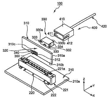
Referring to Figs. 1 to 3, description will proceed to a photoelectric
conversion/connection device 100 according to the first embodiment of this
invention. Fig. 1 is an exploded perspective view showing the photoelectric
conversion/connection device 100. Fig. 2 is an exploded perspective view
showing the photoelectric conversion/connection device 100 disassembled into
respective components. Fig. 3 is an assembled perspective view of the
photoelectric conversion/connection device 100.
[0021]
In the illustrated example, a coordinate system has a first or X direction
extending leftward and rightward, i.e. laterally, a second or Y direction
extending
forward and backward, and a third or Z direction extending upward and
downward. The first to third directions X, Y, and Z are perpendicular to each
other. The first or X direction is also called a lateral or width direction.
The
second or Y direction is also called a fore-and-aft direction. The third or Z
direction is also called an up-and-down direction.
[0022]
As shown in Fig. 2, the photoelectric conversion/connection device 100
comprises three components (constituent members), i.e. a motherboard
assembly 200, a sub-board assembly 300, and an optical connector 400.
[0023]
The motherboard assembly 200 comprises a motherboard 210 and an
CA 02676381 2009-07-23
10
electrical connector 220. The motherboard 210 has a flat-plate shape
extending parallel to an XY plane defined by the X and Y directions. The
motherboard 210 has a main surface 210a mounted with the later-described
electrical connector 220 thereon and formed with circuits (not illustrated)
and
patterns (not illustrated) thereon.
[0024]
The electrical connector 220 is surface-mounted on the main surface
210a of the motherboard 210. The electrical connector 220 comprises a
receptacle (socket) connector. The electrical connector 220 has a generally
rectangular parallelepiped housing 221. The housing 221 has an elongated
shape extending in the X direction. The housing 221 has a rectangular fitting
groove 221a extending in the X direction. The fitting groove 221a is for
insertion of an end portion of a sub-board 310 of the later-described sub-
board
assembly 300.
[0025]
The illustrated electrical connector 220 is mounted on the main surface
210a of the motherboard 210 in an upright manner.
[0026]
The housing 221 holds a plurality of contacts 222 in the fitting groove
221a. These contacts 222 are arranged at regular intervals in the X direction.
Terminal portions, on the side facing the main surface 210a of the motherboard
210, of the contacts 222 are bent at 90 degrees as shown in Fig. 1.
[0027]
The electrical connector 220 is fixed on the main surface 210a of the
motherboard 210 by soldering the terminal portions of the contacts 222 to pads
(not shown) formed on the main surface 210a of the motherboard 210. That is,
the electrical connector 220 is surface-mounted on the main surface 210a of
the
motherboard 210, thereby forming the motherboard assembly 200. Such an
CA 02676381 2009-07-23
11
electrical connector 220 is known in this technical field and is called a card
edge
connector.
[0028]
The sub-board assembly 300 comprises the sub-board (mounting
board) 310, optical elements 320, and a guide 330. The sub-board 310 has a
flat-plate shape extending parallel to an XZ plane defined by the X and Z
directions. The sub-board 310 extends in the X direction.
[0029]
The sub-board 310 has a first surface (first mounting surface) 310a and
a second surface (second mounting surface) 310b opposite to each other in a
thickness direction (Y direction) thereof. The guide 330 is mounted on the
first
surface (first mounting surface) 310a as described later and the optical
elements 320 are mounted on the second surface (second mounting surface)
310b as described later.
[0030]
The sub-board 310 has a plurality of electrodes 312 on the second
surface (second mounting surface) 310b at its end portion facing the
electrical
connector 220 located in the Z direction. These electrodes 312 are arranged
at regular intervals in the X direction. It is to be noted that although only
six
electrodes 312 are shown in Figs. 1 to 3, the electrodes 312 are actually
provided at positions corresponding to the above contacts 222. In other words,
the number of the electrodes 312 is equal to that of the contacts 222.
[0031]
Therefore, when the end portion of the sub-board 310 is inserted (fitted)
into the fitting groove 221a of the electrical connector 220, the plurality of
electrodes 312 of the sub-board 310 are electrically connected to the
corresponding contacts 222 of the electrical connector 220, respectively.
Thus,
the sub-board 310 is electrically connected to the motherboard 210 through the
CA 02676381 2009-07-23
12
contacts 222 of the electrical connector 220.
[0032]
The sub-board 310 has holes 310c each formed in the thickness
direction (Y direction) thereof. Although only the single hole 310c is shown
in
Fig. 1, the sub-board 310 actually has four holes 310c in this example.
[0033]
The guide 330 has one end portion 330a and another end portion 330b
opposite to each other in the thickness direction (Y direction) of the sub-
board
(mounting board) 310. The guide 330 is mounted, at the one end portion 330a
thereof, on the first surface (first mounting surface) 310a of the sub-board
(mounting board) 310.
[0034]
Fig. 4 shows a perspective view of the guide 330 and Fig. 5 shows a
perspective sectional view of the guide 330. Figs. 4 and 5 omit illustration
of a
later-described pair of projecting portions. The guide 330 has four through
holes 331 each extending in the thickness direction (Y direction) of the
sub-board (mounting board) 310. Each through hole 331 is divided into a hole
331a on one end side and a hole 331b on the other end side. The guide 330
incorporates therein a first optical fiber 332 fixed in the hole 331a on the
one
end side of each through hole 331.
[0035]
Although only the single first optical fiber 332 is shown in Figs. 4 and 5,
the guide 330 actually incorporates four first optical fibers 332 therein. The
first optical fiber 332 is also called a guide-side optical fiber. Each first
optical
fiber (guide-side optical fiber) 332 has a protruding portion 332a protruding
from
the one end portion 330a by a length substantially equal to the thickness of
the
sub-board (mounting board) 310.
[0036]
CA 02676381 2009-07-23
13
The diameter of each hole 310c formed in the sub-board (mounting
board) 310 is slightly greater than the outer diameter of the first optical
fiber
(guide-side optical fiber) 332.
[0037]
The guide 330 is mounted on the first surface (first mounting surface)
310a of the sub-board (mounting board) 310 in a state where the protruding
portions 332a are inserted into the holes 310c of the sub-board (mounting
board) 310.
[0038]
Specifically, the guide 330 is attached with a pair of L-shaped terminals
333 on both side surfaces 330c, in the lateral direction (X direction), of the
guide
330 on the one end portion 330a side. By soldering the pair of terminals 333
of the guide 330 to a pair of pads (not shown) formed on the first surface
(first
mounting surface) 310a of the sub-board (mounting board) 310, the guide 330
is fixed on the first surface (first mounting surface) 310a of the sub-board
(mounting board) 310. That is, the pair of terminals 333 serve to
surface-mount the guide 330 on the first surface (first mounting surface) 310a
of
the sub-board (mounting board) 310.
[0039]
As shown in Figs. 1 and 2, the guide 330 has a pair of projecting
portions 334 on both side surfaces 330c, in the lateral direction (X
direction), of
the guide 330 on the other end portion 330b side. The pair of projecting
portions 334 are for locking the later-described optical connector 400.
[0040]
As shown in Fig. 5, the other end portion 332b of the first optical fiber
(guide-side optical fiber) 332 extends only to the middle portion of the guide
330.
A second optical fiber (connector-side optical fiber) fixed to the later-
described
optical connector 400 is inserted into the hole 331b on the other end side of
CA 02676381 2009-07-23
14
each through hole 331. The diameter of each through hole 331 is slightly
greater than the outer diameter of the second optical fiber (connector-side
optical fiber). Accordingly, the hole 331b on the other end side of each
through
hole 331 serves as an aligning portion for aligning the first optical fiber
(guide-side optical fiber) 332 fixed to the guide 330 and the second optical
fiber
(connector-side optical fiber) fixed to the optical connector 400. Herein,
"aligning" represents substantially aligning optical axes of two optical parts
(two
optical fibers in this case) with each other.
[0041]
The optical elements 320 are mounted on the second surface (second
mounting surface) 310b of the sub-board (mounting board) 310 at positions of
the holes 310c of the sub-board (mounting board) 310 so as to be optically
coupled to the first optical fibers (guide-side optical fibers) 332,
respectively.
[0042]
Referring to Figs. 6 to 8, a description will be given of the case where,
after mounting the guide 330 on the first surface (first mounting surface)
310a of
the sub-board (mounting board) 310 by inserting the protruding portions 332a
of
the first optical fibers (guide-side optical fibers) 332, fixed to the guide
330, into
the holes 310c of the sub-board (mounting board) 310, the optical element 320
is mounted on the second surface (second mounting surface) 310b of the
sub-board (mounting board) 310 while being aligned. Fig. 6 is a perspective
view showing a state where the guide 330 is mounted on the first surface
(first
mounting surface) 310a of the sub-board (mounting board) 310. Fig. 7 is a
perspective view showing a state before mounting the optical element 320 on
the second surface (second mounting surface) 310b of the sub-board (mounting
board) 310 and Fig. 8 is a perspective view showing a state after mounting the
optical element 320 on the second surface (second mounting surface) 310b of
the sub-board (mounting board) 310.
CA 02676381 2009-07-23
15
[0043]
The optical element 320 may be a light-emitting element such as a laser
diode (LD) or a light-receiving element such as a photodiode (PD). A driver
340 for driving the optical element 320, a capacitor 350, and so on are
mounted
on the second surface (second mounting surface) 310b of the sub-board
(mounting board) 310.
[0044]
When the optical element 320 comprises a light-emitting element, an
optical power meter is connected to an end portion of an optical cable of the
optical connector 400 connected to the guide 330 as described later. On the
other hand, when the optical element 320 comprises a light-receiving element,
a
light source is connected to an end portion of an optical cable of the optical
connector 400 connected to the guide 330.
[0045]
It will be assumed that the optical element 320 comprises a
light-emitting element. In this case, by driving the light-emitting element
320, a
laser beam emitted from the light-emitting element 320 passes through the
first
optical fiber 322 (guide-side optical fiber) of the guide 330 and the second
optical fiber (connector-side optical fiber) of the optical connector 400 so
that
the quantity of light is measured by the optical power meter. At a position
where the quantity of light measured by the optical power meter becomes
maximum, the optical element (light-emitting element) 320 is fixed on the
second surface (second mounting surface) 310b of the sub-board (mounting
board) 310 by soldering, an adhesive, or the like.
[0046]
It will be assumed that the optical element 320 comprises a
light-receiving element. In this case, a laser beam emitted from the
above-mentioned light source passes through the second optical fiber
CA 02676381 2009-07-23
16
(connector-side optical fiber) of the optical connector 400 and the first
optical
fiber 322 (guide-side optical fiber) of the guide 330 and is received by the
light-receiving element 320. The coupling loss or the like in the amount of
received light at the light-receiving element 320 is detected by a detector
(not
illustrated). At a position where the loss is small, the optical element
(light-receiving element) 320 is fixed on the second surface (second mounting
surface) 310b of the sub-board (mounting board) 310 by an adhesive or the
like.
[0047]
In this manner, the optical element 320 is mounted on the second
surface (second mounting surface) 310b of the sub-board (mounting board) 310
while being aligned. That is, it is possible to substantially align the
optical axis
of the optical element 320 and the optical axis of the first optical fiber
(guide-side optical fiber) 332 with each other.
[0048]
Referring to Figs. 9 and 10, the structure of the optical connector 400
will be described. Fig. 9 is an exploded perspective view of the optical
connector 400 and Fig. 10 is an assembled perspective view of the optical
connector 400.
[0049]
The optical connector 400 comprises an optical connector body 410
and an optical cable 420. The optical connector body 410 has a generally
rectangular parallelepiped external shape. The optical connector body 410
has a guide receiving portion 411 for receiving the guide 330 therein.
Further,
the optical connector body 410 has, at its both side walls in the X direction,
a
pair of engaging claws 412 that engage with the pair of projecting portions
334
of the guide 330. Anyway, the optical connector body 410 comprises a
socket-type connector.
[0050]
CA 02676381 2009-07-23
17
A through hole (not shown) into which the optical cable 420 is inserted
is provided at a bottom portion 410a of the optical connector body 410. The
optical cable 420 extends in the Y direction and includes second optical
fibers
(connector-side optical fiber) 421. Although only the single second optical
fiber
(connector-side optical fiber) 421 is shown in Fig. 9, the optical cable 420
actually includes four second optical fibers (connector-side optical fibers)
in this
example.
[0051]
The amount of protrusion of the second optical fiber (connector-side
optical fiber) 421 from the optical cable 410 is substantially equal to the
length
of the hole 331b on the other end side of the through hole 331 (i.e. the
aligning
portion) formed in the guide 330 (see Fig. 5).
[0052]
Referring to Figs. 11 to 15, a description will be given of the case of
connecting the optical connector 400 to the guide 330. Fig. 11 is a
perspective
sectional view showing a state after mounting the guide 330 on the sub-board
(mounting board) 310, together with the optical connector. Fig. 12 is a
perspective view showing a state where the optical connector 400 is connected
to the guide 330. Fig. 13 is a perspective view showing a state before
connecting the optical connector 400 to the guide 330 and Fig. 14 is a
perspective view showing a state after connecting the optical connector 400 to
the guide 330. Fig. 15 is a perspective sectional view of Fig. 14. Figs. 13 to
15 omit illustration of the pair of terminals 333 (Fig. 4) attached to both
side
surfaces 330c of the guide 330.
[0053]
As shown in Fig. 11, the second optical fibers 421 are fixed to the
optical connector 400 through the optical cable 420. On the other hand, the
first optical fibers 332 are fixed to the guide 330. The optical connector 400
is
CA 02676381 2009-07-23
18
connected to the guide 330 in a state where the second optical fibers 421 are
inserted into the aligning portions 331b of the guide 330. In this event, the
tips
421a (Fig. 9) of the second optical fibers (connector-side optical fibers) 421
butt
against the other end portions 332b (Fig. 5) of the first optical fibers
(guide-side
optical fibers) 332.
[0054]
Further, in this event, as shown in Fig. 15, the pair of engaging claws
412 of the optical connector body 410 engage with the pair of projecting
portions 334 of the guide 330 so that the optical connector 400 is locked to
the
guide 330.
[0055]
In this embodiment, the second optical fibers 421 are fixed to the optical
connector 400 by fixing the optical cable 420 to the optical connector body
410.
However, the second optical fibers 421 may be fixed to the optical connector
400 by directly fixing the second optical fibers 421 to the optical connector
body
410.
[0056]
In the photoelectric conversion/connection device 100 according to the
first embodiment of this invention described above, inasmuch as the optical
elements 320 are exposed as shown in Fig. 3, the heat generated in the optical
elements 320 can be dissipated to the outside. Further, as indicated by a big
arrow in Fig. 3, inasmuch as a member excellent in thermal conductivity (e.g.
aluminum) can be directly attached to the optical elements 320, it is possible
to
improve the heat dissipation of the optical elements 320. Inasmuch as each
optical element 320 is directly aligned with the medium (first optical fiber
332),
there is also an advantage in that even if the accuracy of members of the
respective optical elements 320 is poor, it is possible to fabricate the
photoelectric conversion/connection device 100. Further, as shown in Fig. 2,
CA 02676381 2009-07-23
19
inasmuch as the photoelectric conversion/connection device 100 is composed
of the three components (constituent members), i.e. the motherboard assembly
200, the sub-board assembly 300, and the optical connector 400, when there is
a problem (damage, failure, degradation) in the individual components
(constituent members), it is possible to easily replace them. Inasmuch as the
electrical connector 220 mounted on the main surface 210a of the motherboard
210 is capable of detachably connecting the sub-board (mounting board) 310
thereto, it is possible to easily attach and detach the sub-board (mounting
board) 310 with respect to the motherboard 210.
[0057]
Referring to Fig. 16, the description will proceed to a photoelectric
conversion/connection device 100A according to the second embodiment of this
invention. Fig. 16 is a schematic side view showing the photoelectric
conversion/connection device 100A.
[0058]
Also in the illustrated example, a coordinate system has a first or X
direction extending leftward and rightward, i.e. laterally, a second or Y
direction
extending forward and backward, and a third or Z direction extending upward
and downward.
[0059]
The illustrated photoelectric conversion/connection device 100A has the
same structure as the photoelectric conversion/connection device 100
according to the first embodiment of this invention described above, except
that
the structure of a motherboard assembly is modified as described later. In
view of this, a reference symbol of 200A is assigned to the motherboard
assembly. The same reference symbols are assigned to components having
the same functions as those of the photoelectric conversion/connection device
100 described above.
CA 02676381 2009-07-23
20
[0060]
The motherboard assembly 200A has the same structure as the
motherboard assembly 200 except that an electrical connector is modified as
described later. In view of this, a reference symbol of 220A is assigned to
the
electrical connector.
[0061]
The electrical connector 220 of the first embodiment is mounted on the
main surface 210a of the motherboard 210 in a standing manner in the
perpendicular direction (un-and-down direction) Z, while, the electrical
connector 220A of the second embodiment is mounted on a main surface 210a
of a motherboard 210 in a lay-down manner in the horizontal direction. In
other words, the electrical connector 220 is mounted on the main surface 210a
of the motherboard 210 in an upright manner, while, the electrical connector
220A is mounted on the main surface 210a of the motherboard 210 in a
transverse manner.
[0062]
Therefore, in the electrical connector 220, the fitting groove 221a is
open at its upper portion along the up-and-down direction Z, while, in the
electrical connector 220A, its fitting groove (not illustrated) is open at its
back
portion (rear portion) along the fore-and-aft direction Y.
[0063]
In the photoelectric conversion/connection device 100, the sub-board
310 is connected to the electrical connector 220 so as to extend in a
direction
(vertical direction) perpendicular to a direction (horizontal direction) in
which the
motherboard 210 extends, while, in the photoelectric conversion/connection
device 100A, a sub-board 310 is connected to the electrical connector 220A so
as to extend in a direction (horizontal direction) parallel to a direction
(horizontal
direction) in which the motherboard 210 extends.
CA 02676381 2009-07-23
21
[0064]
In the photoelectric conversion/connection device 100A, a first surface
(first mounting surface) 310a of the sub-board 310 becomes a lower surface
and a second surface (second mounting surface) 310b thereof becomes an
upper surface. Therefore, as shown in Fig. 16, optical elements 320 are
mounted on the second surface 310b being the upper surface of the sub-board
310.
[0065]
Also in the photoelectric conversion/connection device 100A according
to the second embodiment of this invention, inasmuch as the optical elements
320 are exposed, the heat generated in the optical elements 320 can be
dissipated to the outside. Further, inasmuch as a member excellent in thermal
conductivity (e.g. aluminum) can be directly attached to the optical elements
320, it is possible to improve the heat dissipation of the optical elements
320.
Inasmuch as each optical element 320 is directly aligned with a medium (first
optical fiber 332), there is also an advantage in that even if the accuracy of
members of the respective optical elements 320 is poor, it is possible to
fabricate the photoelectric conversion/connection device 100A. Further,
inasmuch as the photoelectric conversion/connection device 100A is composed
of three components (constituent members), i.e. the motherboard assembly
200A, a sub-board assembly 300, and an optical connector 400, when there is a
problem (damage, failure, degradation) in the individual components
(constituent members), it is possible to easily replace them. Inasmuch as the
electrical connector 220A mounted on the main surface 210a of the
motherboard 210 is capable of detachably connecting the sub-board (mounting
board) 310 thereto, it is possible to easily attach and detach the sub-board
(mounting board) 310 with respect to the motherboard 210.
[0066]
CA 02676381 2009-07-23
22
In the photoelectric conversion/connection device 100, 100A according
to this invention described above, the mounting board 310 may have the first
surface 310a and the second surface 310b opposite to each other in the
thickness direction of the mounting board 310 and may have the hole 310c
formed in the thickness direction of the mounting board 310. In this case, the
photoelectric conversion/connection device 100, 100A is preferably provided
with the guide 330 that is mounted, at its one end portion 330a, on the first
surface 310a of the mounting board 310 and is connectable to the optical
connector 400 on the other end portion 330b side. The guide 330 has the
through hole 331 extending in the thickness direction of the mounting board
310.
The guide 330 incorporates therein the guide-side optical fiber 332 fixed in
the
through hole 331. The guide-side optical fiber 332 has the protruding portion
332a protruding from the one end portion 330a by the length substantially
equal
to the thickness of the mounting board 310. The protruding portion 332a is
inserted into the hole 310c of the mounting board 310. The optical element
320 is mounted on the second surface 310b of the mounting board 310 at the
position of the hole 310c of the mounting board 310 so as to be optically
coupled to the guide-side optical fiber 332. The optical connector 400 may
include the connector-side optical fiber 421 fixed to the optical connector
400 so
as to be optically coupled to the guide-side optical fiber 332. The guide 330
preferably has, on the other end portion 330b side, the aligning portion 331b
for
connecting the guide-side optical fiber 332 and the connector-side optical
fiber
421 to each other. The connector-side optical fiber 421 may be inserted into
the through hole 331 of the guide 330 and the aligning portion 331b may be the
through hole 331 of the guide 330.
[0067]
The photoelectric conversion/connection device 100, 100A according to
this invention described above may further comprise the motherboard 210
CA 02676381 2009-07-23
23
having the main surface 210a and the electrical connector 220, 220A mounted
on the main surface of the motherboard and capable of detachably connecting
the mounting board 310 thereto. In this case, the mounting board 310 may be
connected to the electrical connector 220 so as to extend in the direction
perpendicular to the extending direction of the motherboard 210 or may be
connected to the electrical connector 220A so as to extend in the direction
parallel to the extending direction of the motherboard 210.
[0068]
While the present invention has been described with reference to the
embodiments thereof, the present invention is not limited to the above
embodiments. It will be understood by those of ordinary skill in the art that
various changes in structure and details may be made without departing from
the scope of the present invention. For example, although the sub-board
(mounting board) 310 is formed with the four holes 310c in the above
embodiments, the number of the holes 310c is not limited to four, but may be
any number equal to or greater than one. Likewise, although the guide 330 is
formed with the four through holes 331 in the above embodiments, the number
of the through holes 331 is also not limited to four, but may be any number
equal to or greater than one.