Note: Descriptions are shown in the official language in which they were submitted.
CA 02676748 2009-08-27
- ~ -
DEFECT MARKING METHOD AND DEVICE
This application is a divisional of Canadian Patent
Application No. 2,365,879 filed March 15, 2000.
FIELD OF THE INVENTION
The present invention relates to a method for marking
defect on a steel sheet in a steel making process line and to
a device therefor.
DESCRIPTION OF RELATED ARTS
Cold-rolled steel sheets manufactured by cold-rolling are
subjected to inspection of surface defects over the whole length
of coil thereof for quality assurance. JP-A-5-196581, (the term
"JP-A" referred herein signifies the "Unexamined Japanese patent
publication" ), discloses a method for detecting surface defects
and internal defects of steel sheets. According to the
disclosure, detection of the surface defects on a steel sheet
is conducted by scanning the surface of steel sheet which is
running through a manufacturing line, in width direction thereof
by laser light, by converting the reflected light to voltage
intensity using a photoelectric transfer device such as CCD
element, then by judging the presence/absence and the degree of
the defect based on the voltage signals. The internal defects
of a steel sheet are detected by computing the defect depth in
the thickness direction of the steel sheet and the defect size
using a magnetic particle tester. Usually, the result of the
defect inspection is displayed on a CRT or the like as information
CA 02676748 2009-08-27
- 2 -
in terms of defect position, defect name, defect grade, and the
like, or is printed in a document.
It is impossible to obtain products completely free from
defects. Consequently, the products are shipped after removing
portions of harmful defect for the buyer concerned on the basis
of the defect information displayed on a CRT or the like in the
manufacturing line, or after removing the portions of harmful
defect for the buyer concerned by applying re-inspection in
succeeding stage on the basis of the above-described defect
information. Alternatively, a document of the above-described
harmful detect information is submitted to the buyer concerned,
together with the coil that contains harmful defect portions,
thus letting the buyer remove the harmful defects.
In the case that the harmful defect portions are removed
in the manufacturing line or in succeeding stage, since there
is no definite standard of the degree of harm for the surface
defects, the removal of harmful defect portions is an action
practiced excessively from the standpoint of quality assurance.
Also there are cases of not-removing harmful defects caused from a
miss-judgment such as overlooking and from a state of very close
to undeterminable defect. Furthermore, removal of harmful defect
portions raises problems such as reduction in the coil weight and
reduction in the work efficiency of the buyer.
On the other hand, the buyer needs to work on coils while
referring the documented data of defect information, which
induces troublesome work and, in some cases, may result in
treatment of coils leaving defects non-detected.
CA 02676748 2009-08-27
- 3 -
JP-A-4-291138 discloses a marking device that sprays a
paint on flawed portions of steel sheets. According to the
disclosure, marking is done by spraying a paint to flawed portions
of the steel sheets detected by a flaw detection device, thus
enabling the buyer to readily identify the flawed portio.n on
re-inspection by the buyer.
Since, however, the method for marking according to
JP-A-4-291138 does not give confirmation whether the marking was
correctly given or not, and an abnormal marking induces further
troubles to the buyer. In addition, paint spray generates shade
of color on marking, which may induce dents, in an area with large
quantity of applied paint, even at normal portions after the paint
is dried. For the case of spray marking, an oiled steel sheet
cannot leave any marking on the surface thereof because the paint
is sprayed on an oil film, though that kind of problem does not
occur on a steel sheet free of applied oil. When marking is given
on all of the flawed portions,, the marking is also given to
harmless defects to the buyer, which induces disadvantages
including reduction in work efficiency.
There are inspection methods for surface defects,
disclosed in JP-A-58-204353, JP-A-60-228943, JP-A-8-178867,
JP-A-57-166532, and JP-A-9-166552. All of these disclosed
methods aim to detect flaws having significant surface
irregularity or to detect flaws with the presence of foreign
matter such as oxide film. Thus, for pattern-like scabbed flaws
or the like which do not have significant surface irregularity,
these methods cannot surely identify all the flaws.
CA 02676748 2009-08-27
- 4 -
As means for applying marking to flawed portions and
singular parts generated on a metal material, there are
commercially available apparatuses such as ink jet printer and
ink dot marking device.
When an ink jet printer is used, kinds and colors of ink
are limited because special inks are required owing to various
conditions such as charging the inks. Nevertheless, when the
manufactured metal materials are used for automobile steel sheets,
ink performance and color may be specified for convenience of
customer's inspection.
For example, if an ink is under limitations such that the
ink should have excellent quick drying property, the ink should
not be blotting on applying oil, and the ink should be blue,
respective special inks should be developed to satisfy the
customer's conditions. The development of that special inks
needs long time and much money, which is difficult to practically
respond to the request.
In addition, since the ejection part of the ink is necessary
to maintain clean, significant cost and time should be consumed
for maintenance. Accordingly, when an ink jet printer is used,
a special ink has to be used, so that color and kind of the ink
cannot readily be changed.
SUMMARY OF THE INVENTION
It is an object of the present invention to provide a method
for defect marking that readily and surely identifies harmful
defects, and an apparatus therefor.
CA 02676748 2009-08-27
- 5 -
It is another object of the present invention to provide
a surface flaw marking device that detects pattern-like scabs
having no significant surface irregularity such as surface crack,
burr, and curl up, thus allowing to notifying the defect
information to the user concerned with a simple means, also to
provide a metal strip with marking, and to provide a method for
manufacturing thereof.
To attain the objects, firstly, the present invention
provides a method for marking defect, which comprises the steps
of:
(a) installing a surface defect tester to detect surface
flaw and a marker device to apply marking at defect position,
in a continuous processing line of steel sheet;
(b) detecting the surface flaw on the steel sheet using
the surface defect tester;
(c) calculating to determine defect name, defect grade,
defect length, and defect position in width direction of the steel
sheet, on the basis of thus detected flaw information, further
identifying the defect in terms of harmful defect, undeterminable
defect, and harmless defect;
(d) tracking the defect position for each of the harmful
defect and the undeterminable defect; and
(e) marking the defect position at a moment that the defect
reaches the marker device.
Secondly, the present invention provides a method for
defect marking, which comprises the steps of:
(a) calculating to determine defect name, defect grade,
CA 02676748 2009-08-27
- 6 -
defect length, and defect position in width direction of a coil
for a surface defect thereon, in a processing line provided with
a surface defect tester, further identifying the defect in terms
of harmful defect and undeterminable defect;
(b) feeding the coil to a steel sheet continuous processing
line provided with a marker device for applying marking; and
(c) marking to the defect position at a moment that the
harmful defect or the undeterminable defect reaches the marker
device, on the basis of the information of preliminarily
identified harmful defect or undeterminable defect.
Thirdly, the present invention provides a flaw inspection
device, which comprises:
a plurality of light-receiving devices that identify
reflected lights coming from an inspection plane of a metal strip
under two or more of optical comditions different from each other;
and
a signal processing section that judges presence/absence
of surface flaw on the inspection plane, based on a combination
of reflected light components identified under these optical
conditions different from each other.
Fourthly, the present invention provides a defect marking
device, which comprises:
a flaw inspection means comprising plurality of light-
receiving parts that identify reflected lights coming from an
inspection plane of a metal strip under two or more of optical
conditions different from each other, and a signal processing
section that judges presence/absence of surface flaw on the
CA 02676748 2009-08-27
- 7 -
inspection plane based on a combination of reflected light
components identified under these optical conditions different
from each other; and
a marking means that applies marking that indicates
information relating to the flaw on the surface of the metal strip.
Fifthly, the present invention provides a method for
manufacturing metal strip with defect marking, which comprises
the steps of:
(a) identifying reflected lights coming from an
inspection plane of a metal strip under two or more of optical
conditions different from each other;
(b) judging presence/absence of surface flaw on the
inspection plane based on a combination of reflected light
components identified; and
(c) marking information relating to the flaw on the
surface of the metal strip based on the judgment result.
Sixthly, the present invention provides a method for
working metal strip, which comprises the steps of:
(a) identifying reflected lights coming from an
inspection plane of a metal strip under two or more of optical
conditions different from each other;
(b) judging presence/absence of surface flaw on the
inspection plane based on a combination of reflected light
components identified;
(c) marking information relating to the flaw on the
surface of the metal strip;
(d) winding the marked metal strip to prepare a coil;
CA 02676748 2009-08-27
- 8 -
(e) rewinding the coil to detect the marking, and
specifying a specific range of the metal strip based on the
information given by the marking; and
(f) applying specified working to a residual portion of.
the metal strip after avoiding or removing the specified range.
Seventhly, the present invention provides a metal strip
with marking, which has, on a portion that shows an abnormality
compared with a portion of normal combination of surface
reflected light components separated under two or more optical
conditions different from each other, marking indicating
information relating to a flaw on the surface thereof.
Eighthly, the present invention provides a metal strip with
marking, which has, on a portion that gives an abnormal quantity
of light for one or both components of a specular reflection
component on surface and a specular-diffuse reflection component
on plurality of micro-area reflection surfaces, a marking
indicating information relating thereto.
Ninthly, the present invention provides a marking device
for applying marking a flawed portion and a singular part on an
inspection body, detected by an inspection device, comprises
a marker pen;
a penholder to which the marker-pen is detachably mounted;
a penholder lifting mechanism for ascending/descending the
penholder together with the marker-pen;
a protective cap being capable of opening/closing to
protect a pen tip of the marker-pen; and
a shutter mechanism to open/close the protective cap
CA 02676748 2009-08-27
- 9 -
linking with the penholder lifting mechanism.
Tenthly, the present invention provides a marking device
for applying marking a flawed portion and a singular part on a
metal member, detected by an inspection device in a continuous
manufacturing line of a metal material, comprises:
a marker pen;
a penholder to which the marker-pen is detachably mounted;
a penholder lifting mechanism for ascending/descending the
penholder together with the marker-pen;
a protective cap being capable of opening/closing to
protect a pen tip of the marker-pen; and
a shutter mechanism to open/close the protective cap
linking with the penholder lifting mechanism.
CA 02676748 2009-08-27
- 10 -
BRIEF DESCRIPTION OF THE DRAWINGS
Figs. la and lb illustrate an arrangement of main
facilities of the first coiling line for steel sheet
relating to the Best Mode 1 according to the present
invention.
Figs. 2a and 2b illustrate an arrangement of main
facilities of the second coiling line for steel sheet
relating to the Best Mode 1 according to the present
invention.
Figs. 3a and 3b illustrate an arrangement of main
facilities of the third coiling line for steel sheet
relating to the Best Mode 1 according to the present
invention.
Figs. 4a and 4b illustrate an arrangement of main
facilities of the fourth coiling line for steel sheet
relating to the Best Mode 1 according to the present
invention.
Fig. 5 is an example of CRT display relating to the
Best Mode 1 according to the present invention.
Fig. 6 illustrates a relation state between the defect
position and the defect marking position relating to the
Best Mode 1 according to the present invention.
Fig. 7 illustrates an example of arrangement of each
one unit of the defect marking device and the defect marking
detection device, relating to the Best Mode 1 according to
the present invention.
Fig. 8 illustrates an example of arrangement of each
two units of the defect marking device and the defect
marking detection device, relating to the Best Mode 1
according to the present invention.
Fig. 9 illustrate an example of arrangement of each one
CA 02676748 2009-08-27
- 11 -
unit of the defect marking device and the ink drying device,
relating to the Best Mode 1 according to the present invention.
Fig. 10 illustrate an example of arrangement of each one
unit of the defect marking device, the defect marking detection
device, and the ink drying device, relating to the Best Mode 1
according to the present invention.
Fig. 11 illustrate an example of arrangement of each two
units of the defect marking device and the ink drying device,
relating to the Best Mode 1 according to the present invention.
Fig. 12 illustrate an example of arrangement of each two
units of the defect marking device, the defect marking detection
device, and the ink drying device, relating to the Best Mode 1
according to the present invention.
Fig. 13 illustrates an example of applying marking on
defect portions using a single unit of defect marking device
relating to the Best Mode 1 according to the present invention.
Fig. 14 illustrates an example of applying marking
separately on a harmful defect and an undeterminable defect using
two units of defect marking device relating to the Best Mode 1
according to the present invention.
Fig. 15 illustrates an example of arrangement of main
facilities of a processing line provided with a defect marking
device and a defect marking detection device relating to the Best
Mode 1 according to the present invention.
Fig. 16 illustrates an example of arrangement of main
facilities of another processing line provided with a defect
marking device and a defect marking detection device relating
CA 02676748 2009-08-27
- 12 -
to the Best Mode 1 according to the present invention.
Fig. 17 illustrates an example of arrangement of main
facilities of a processing line provided with a defect marking
device, a defect marking detection device, further an inspection
table and a defect marking detection device, relating to the Best
Mode 1 according to the present invention.
Fig. 18 illustrates an example of arrangement of main
facilities of a coiling line provided with a defect marking
detection device, relating to the Best Mode 1 according to the
present invention.
Fig. 19 illustrates an example of arrangement of main
facilities of a shear line provided with a defect marking
detection device, relating to the Best Mode 1 according to the
present invention.
Fig. 20 illustrates an example of applying defect marking
on a defect portion, relating to the Best Mode 1 according to
the present invention.
Fig. 21 illustrates an example of applying defect marking
at two points on the same position in the width direction of steel
sheet, independent of the place of defect portion, relating to
the Best Mode 1 according to the present invention.
Fig. 22 illustrates the relative state between the defect
position and the defect marking position, relating to the Best
Mode 1 according to the present invention.
Fig. 23 illustrates an example of applying separate marking
for a harmful defect and an undeterminable defect using two units
of detect marking device, relating to the Best Mode 1 according
CA 02676748 2009-08-27
- 13 -
to the present invention.
Fig. 24 is a block diagram of an example of the devices
relating to the Best Mode 2 according to the present invention.
Fig. 25 is a plan view of an example of metal strip relating
to the Best Mode 2 according to the present invention.
Fig. 26 is a schematic drawing of an example of rough
structure of a surface flaw inspection device for the devices
relating to the Best Mode 2 according to the present invention.
Fig. 27 is a cross sectional schematic drawing of a surface
flaw detection device relating to the Best Mode 2 according to
the present invention.
Fig. 28 illustrates an arrangement of camera units along
the metal width direction, equipped in the surface flaw
inspection device, relating to the Best Mode 2 according to the
present invention.
Fig. 29 illustrates an arrangement of cameras equipped in
a single camera unit, relating to the Best Mode 2 according to
the present invention.
Fig. 30 is a block diagram of another example of the devices
relating to the Best Mode 2 according to the present invention.
Fig. 31 is a block'diagram of an example of the signal
processing section of the devices relating to the Best Mode 2
according to the present invention.
Fig. 32 is a block diagram of further example of the devices
relating to the Best Mode 2 according to the present invention.
Fig. 33 (a) through (c) illustrate examples of light
intensity signals observed by a device relating to the Best Mode
CA 02676748 2009-08-27
- 14 -
2 according to the present invention.
Fig. 34 (a) through (c) illustrate another examples of
light intensity signals observed by a device relating to the Best
Mode 2 according to the present invention.
Fig. 35 (a) through (d) illustrate the method for
manufacturing alloyed zinc plated steel sheet and show detail
cross sectional views of the sheet, relating to the Best Mode
2 according to the present invention.
Fig. 36 shows a schematic cross sectional view of the
tempered part and the non-tempered part on the surface of metal
strip after temper-rolling, illustrating the relation between
the incident light and the reflection light, relating to the Best
Mode 2 according to the present invention.
Fig. 37 (a) through (c) show angle distribution of
reflected light at the tempered part and the non-tempered part,
relating to the Best Mode 2 according to the present invention.
Fig. 38 shows cross sectional views of an alloy zinc plated
steel sheet to illustrate the progress of occurrence of scab,
relating to the Best Mode 2 according to the present invention.
Fig. 39 (a) through (c) show angle distribution of specular
reflection component and specular-diffuse reflection component,
at scabbed portion and mother material, relating to the Best Mode
2 according to the present invention.
Fig. 40 (a) through (c) show the relation between the normal
angle to micro-area element and the area percentage, at scabbed
portion and mother material on the inspection plane, relating
to the Best Mode 2 according to the present invention.
CA 02676748 2009-08-27
- 15 -
Fig. 41 shows the relation between angles of the incident
light, the reflection light, and the like, on a micro-area element
on the inspection plane, relating to the Best Mode 2 according
to the present invention.
Fig. 42 (a) and (b) show the relation between the normal
angle to a micro-area element and the weight function, relating
to the Best Mode 2 according to the present invention.
Fig. 43 (a) and (b) show the relation between individual
incident lights emitted from various positions on the linear
diffusion light source and the responding incident positions on
the inspection plane, relating to the Best Mode 2 according to
the present invention.
Fig. 44 (a) and (b) shows the polarized state of reflection
light coming from a micro-area element in the case that each
incident light coming from the linear diffusion light source is
polarized, relating to the Best Mode 2 according to the present
invention.
Fig. 45 illustrates the reflection light coming from a
micro-area element in the case that the incident light coming
from center part of the linear diffusion light source is polarized,
relating to the Best Mode 2 according to the present invention.
Fig. 46 illustrates the reflection light coming from a
micro-area element in the case that the incident light coming
from a part other than the center part of the linear diffusion
light source is polarized, relating to the Best Mode 2 according
to the present invention.
Fig. 47 illustrates the relation between the normal angle
CA 02676748 2009-08-27
- 16 -
to micro-area element and the elliptic polarized light of the
reflected light, relating to the Best Mode 2 according to the
present invention.
Fig. 48 shows the relation between the normal angle to
micro-area element and the weight function, relating to the Best
Mode 2 according to the present invention.
Fig. 49 shows the relation between the normal angle to
micro-area element and the weight function at various analyzing
angles, relating to the Best Mode 2 according to the present
invention.
Fig. 50 shows the relation between the normal angle to
micro-area element on the inspection plane and the area
percentage, relating to the Best Mode 2 according to the present
invention.
Fig. 51 shows a rough vertical cross sectional view of the
devices relating to the Best Mode 3 according to the present
invention.
Fig. 52 shows a rough plan view of the devices of Fig. 51.
Fig. 53 shows a rough side view of the device of Fig. 51.
Fig. 54 illustrates a steel sheet manufacturing line
provided with the devices relating to the Best Mode 3 according
to the present invention.
Fig. 55 (a) through (c) illustrate the action of the devices
relating to the Best Mode 3 according to the present invention.
Fig. 56 is a rough sketch of a steel sheet manufacturing
line provided with the devices (providing a dryer) relating to
the Best Mode 3 according to the present invention.
CA 02676748 2009-08-27
- 17 -
Fig. 57 illustrates the marking state on a steel sheet
relating to the Best Mode 3 according to the present invention.
CA 02676748 2009-08-27
- 18 -
BEST MODE FOR CARRYING OUT THE INVENTION
Best Mode 1
The main constitution of the Best Mode 1 is the following.
(1) A defect marking method comprises the steps of:
installing a surface defect tester to detect surface flaw, an
ink marker device to apply marking by an ink at defect position,
and an internal defect tester to detect internal defect of a steel
sheet, in a continuous processing line of the steel sheet;
detecting the surface flaw on the steel sheet using the surface
flaw tester; calculating to determine defect name, defect grade,
defect length, and defect position in width direction of the steel
sheet, on the basis of thus detected flaw information, further
identifying the defect in terms of harmful defect, undeterminable
defect, and harmless defect; detecting the internal flaw of the
steel sheet using the internal defect tester; calculating to
determine the defect length and the defect position in the width
direction of the steel sheet, on the basis of thus detected flaw
information, further identifying the defect in terms of harmful
defect and harmless defect; applying tracking of the defect
position for each of the 'harmful defect and the undeterminable
defect; and applying marking with ink to the defect position at
a moment that the defect reaches the ink marker device.
(2) A defect marking method comprises that, in the method
for defect marking of (1), the surface flaw is subjected to
identification of harmful defect, undeterminable defect, and
harmless defect , on the basis of the defect name, the defect grade,
CA 02676748 2009-08-27
- 19 -
the defect length, the defect position in width direction of the
steel sheet, the defect position on each of front face and rear
face of the steel sheet, and the use of the steel sheet, and that
the internal flaw is subjected to identification of harmful
defect and harmless defect, on the basis of the defect length,
the defect position in the width direction of the steel sheet,
and the use of the steel sheet.
(3) A defect marking method comprises that, in a line
provided with a surface defect tester and an internal defect
tester, the surface defect is subjected to calculation to
determine the defect name, the defect grade, the defect length,
and the defect position in width direction of a coil, further
to identification of the defect in terms of harmful defect and
undeterminable defect, and that the internal defect is subjected
to calculation to determine the defect length and the defect
position in the width direction of the coil, further to
identification of the defect in terms of harmful defect and
harmless defect, further that the coil in which the harmful defect
and the harmless defect are identified is fed to a continuous
processing line of steel sheet, provided with an ink marker device
that applies marking with ink, thus applying marking with ink
to the-defect position at a moment that the harmful defect or
the undeterminable defect reaches the marker device, on the basis
of the information of preliminarily identified harmful defect
or undeterminable defect.
(4) A defect marking method comprises that, in the
above-described (1) through (3), an inspector applies re-
CA 02676748 2009-08-27
- 20 -
judgment of defect which was identified as an undeterminable defect
by the surface defect tester to identify harmful defect and
harmless defect, and applies marking with ink to the position
of_ harmful defect.
(5) A defect marking method comprises that, in the
above-described (1) through (4) , an alarm is generated to a defect
that is identified as an undeterminable defect by the surface defect
tester, and an automatic speed reduction is conducted, then an
inspector applies re-judgment on the undeterminable defect.
(6) A defect marking method comprises that, in the
above-described (4) and (5), on applying re-judgment by the
inspector for the defect that is identified as an undeterminable
defect by the surface defect tester, display of the defect image
and display of defect position for the defect are generated.
(7) A defect marking method comprises that, in the
above-described (1) through (7), the position of defect marking
is changed on the basis of the information of defect in the width
direction given by the surface defect tester and by the internal
defect tester.
(8) A defect marking method comprises that, in the
above-described (1) through (7), the position of defect marking
is changed on the basis of the use of the steel sheet.
(9) A defect marking method comprises that, in the
above-described (1) through (8), the marking is applied
separating the harmful defect from the undeterminable defect.
(10) A defect marking method comprises that, in the
above-described (1) through (9), the marking is applied
CA 02676748 2009-08-27
- 21 -
separating the harmful defect from the undeterminable defect by
changing color from each other.
(11) A defect marking method comprises that, in the
above-described (1) through (10), the color of defect marking
is changed with respective grades of steel sheet.
(12) A defect marking method comprises that, in the
above-described (1) through (11), a defect marking detection
device is installed at downstream side of the ink marker device,
thus monitoring the marking state.
(13) A defect marking method comprises that, in the
above-described (1) through (12), the threshold value of the
def ect marking detection device is changed with respective grades
of steel sheet.
(14) A defect marking method comprises that, in the
above-described (1) through (13), the ink marker device and the
defect marking device are installed as a set, thus letting these
devices track the defect marking position.
(15) A defect marking method comprises that, in the
above-described (1) through (14), an ink drying device is
installed at downstream side of the defect marking.
(16) A defect marking method comprises that, in the
above-described (1) through (15), the ink marker device, the
defect marking device, and the ink drying device are installed
as a set, thus letting these devices track the defect marking
position.
(17) A defect marking method comprises that, in the
above-described (1) through (16), the threshold value of harmful
CA 02676748 2009-08-27
- 22 -
defect and of harmless defect is changed with respective uses
of steel sheet.
(18) A method for working a coil with defect marking
comprises that a coil with defect marking marked in accordance
with the method of above-described (1) through (17) is fed to
a facility provided with a defect marking detection device to
reflect the defect information detected by the defect marking
detection device on the defect removal work.
(19) A method for working a coil with defect marking
comprises that, a coil with defect marking marked in accordance
with the method of above-described (1) through (17) is fed to
a facility provided with a defect marking detection device and
a cleaning means, and the defect information detected by the
defect marking detection device is reflected on the defect
removal work, and an inspector applies re-judgment on the
undeterminable defect, then, when the judgment concluded as the
harmless defect , the marking ink is cleaned by the cleaning means.
(20) A defect marking method comprises that, in the
above-described (1) through (19), (excluding (10), (15), and
(16)), an abrasive member marker device that applies marking
using an abrasive member is installed instead of the ink marker
device using ink, thus applying marking with the abrasive member
instead of applying marking with ink.
Figs. 1 through 4 illustrate examples of arrangement of
main facilities of continuous treatment line of steel sheet,
being used in the description of the Best Mode 1 according to
CA 02676748 2009-08-27
- 23 -
the present invention.
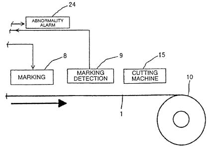
In Fig. 1, the reference number 3 designates a surface
defect tester equipped with a detector 2 each one on front face
and rear face of a steel sheet 1 and with a signal processing
section 4, the reference number 5 designates a CRT, 6 designates
a centralized control panel, 7 designates a secondary judgment
entering device, 8 designates a defect marking device (an ink
marker device), 9 designates a defect marking detection device,
designates a tension reel, 11 designates a transfer roll, 12
designates a pulse generator, 13 designates a arithmetic unit
for detecting steel sheet transfer distance, 14 designates an
external memory device, 15 designates a cutting machine, and 16
designates an inspection table.
Fig. 2 illustrates the facilities of Fig. 1 further
providing a magnetic particle tester (an internal defect tester)
34 equipped with a magnetic sensor 35 which detects internal
defect of the steel sheet 1, and with a signal processing section
36. The facilities of Fig. 3 and Fig. 4 have an ink drying device
40 to dry the marked ink at downstream side of the defect marking
device (ink marker device) 8.
In the facilities shown in Figs. 1 through 4, the detector
2 positioned at each of front face and rear face of the steel
sheet, in the surface defect tester 3, detects flaws that are
candidates of defects on each of front face and rear face of the
steel sheet 1, and sends the detected signals to the signal
processing section 4.
The signal processing section 4 calculates the
CA 02676748 2009-08-27
- 24 -
identification of defect name, defect grade, defect length, and
defect position in the width direction of the steel sheet, based
on the signals obtained from characteristic quantity, exceeding
a specific threshold value of the signals, of defect candidates.
The magnetic sensor 35 of the magnetic particle tester 34
detects an internal defect of the steel sheet 1, and sends the
detected signals to the signal processing section 36. The signal
processing section 36 calculates the identification of defect
length and defect position in the width direction of the steel
sheet, based on the signals obtained from characteristic quantity,
exceeding a specific threshold value of the signals, of defect
candidates, then transmits the calculation result to the signal
processing section 4 of the surface defect tester 3.
Furthermore, calculation of marking command is conducted
based on the marking information sent from a host computer 23,
including the marking target defect name (including internal
defect in the case where the internal defect tester 34 is provided),
defect grade, and edge insensitive zone, for each of front face
and rear face, and on the result of calculation on the basis of
defect information detected by the surface defect tester 3, or
further on the basis of grade and use of the steel sheet.
Both the calculated marking command and the calculated
defect information are displayed on the screen of CRT 5.
Furthermore, the defect generation signal, the defect
information, and the defect position are generated on the
centralized control panel 6.
The rotational speed of the transfer roll 11 that transfers
CA 02676748 2009-08-27
- 25 -
the steel sheet 1 is measured by the pulse generator 12, and the
steel sheet feed length is calculated by the arithmetic unit for
detecting steel sheet transfer distance 13, then the result is
generated to the centralized control panel 6. The centralized
control panel 6 edits the above-described defect information,
identifies harmful defect and undeterminable defect, (harmful
defect for internal defect: and so forth) , based on the defect
name and the defect grade, and furthermore, if needed, identifies
harmful defect and undeterminable defect considering the defect
position information and the use of the steel sheet for each of
front face and rear face. If necessary, the centralized control
panel 6 gives judgment of necessity of marking for the harmful
defect and the identified undeterminable defect which were
identified.
The centralized control panel 6 tracks the defect position
based on the feed length of steel sheet transmitted from the
arithmetic unit for detecting steel sheet transfer distance 13,
and generates alarm of arriving the undeterminable defect at the
re-judgment place (inspection table). If necessary, automatic
speed reduction is given, and the defect image is displayed on
CRT 5, thus easing the defect judgment of worker.
When a defect portion arrives at the secondary judgment
place (inspection table) 16, the worker conducts the secondary
judgment under visual inspection, and confirms the detection
result of the surface defect tester 3 on the CRT 5, thus giving
conclusion of correct/incorrect result. If the result differs
in the comparison, correction is given, and the corrected result
CA 02676748 2009-08-27
- 26 -
is entered to the secondary judgment entering device 7, further
is generated to the centralized control panel 6. Fig. 5 is an
example of CRT display. The defect information given in the
figure is the information of the surface defect tester 3, and
the blank column in the figure is the place to enter the secondary
judgment result.
The centralized control panel 6 conducts re-edition of the
above-described defect information on the basis of the corrected
information, and identifies harmful defect and undeterminable
defect based on the defect name and defect grade. Furthermore,
the centralized control panel 6 conducts tracking of the
positions of harmful defect and undeterminable defect,( the defect
judged to have marking in the case that the judgment of
presence/absence of marking is given), based on the feed length
of the steel sheet 1 obtained from the rotational speed of the
transfer roll 11, thus moves the defect marking device 8 and the
defect marking detection device 9 to a place of defect before
the defect portion passes through the defect marking device 8.
Then, the centralized control panel 6 generates a start signal
to start the defect marking device 8 at the moment that the defect
part passes through the defect marking device 8.
Based on the above-described start signal, the defect
marking device 8 starts, thus conducting marking on the harmful
defect and the undeterminable defect synchronously with the timing
that the harmful defect and the undeterminable defect pass through
the defect marking device 8.
The defect marking device 8 begins applying marking at a
CA 02676748 2009-08-27
- 27 -
moment of receiving the marking command. Marking is given by
applying ink onto the steel sheet 1 by directly pressing a felt
impregnated with ink against the steel sheet 1. Even on a coil
applied with oil, marking is surely applied on the surface of
the steel sheet. Since there is no problem of shading in color,
which occurs in paint coating, no dent appears on the surface
of the steel sheet. The felt wears by direct contact with the
steel sheet 1. If the marking exceeds a standard length, the
centralized control panel 6 generates an alarm to notify the
worker to replace the felt.
Considering the tracking accuracy of the defect position,
the marking length is set so as the defect portion not to come
outside of the defect marking. The facility adds 0.5 m to the
defect length judged by the centralized control panel 8 on each
of front and rear edges of the defect, taking into account of
the tracking information, and generates a command for applying
marking by 1 m longer than the actual defect length. If the defect
is a pattern of point-like defects each having not more than
several millimeters in length, the command is to apply marking
by adding 0.25 m to each of front and rear edges of the defect.
For the length of marking, it is preferred to determine
thereof under a negotiation with the buyer concerned. The
centralized control panel 6 conducts monitoring of allowable
number of markings and allowable length of marking, as additional
control items. If these monitoring values exceed allowable limit,
the centralized control panel 6 generates an abnormality alarm
to an alarm device 24.
CA 02676748 2009-08-27
- 28 -
The host computer 23 conducts control of individual
coils on the basis of the information coming from the
centralized control panel 6, and gives judgment of shipment.
Fig. 6 shows a state of the defect position and the
defect marking position. The harmful defect 20 is within the
display range of the defect marking 21 in the length
direction.
From the standpoint of easiness in visual detection and
of easiness in detection by the defect marking detection
device 9, the line width of the marking is most preferably in
a range of from 3 to 10 mm. From the point of felt wear and
ink visibility, the pressing force of felt is most preferably
in a range of from 150 to 500 g, wherein the pressing force
is expressed by the equation:
PRESSING FORCE (g) = [Pressing Force by Air Cylinder g/cmz)]x
[Area of Felt (cmz) ] + [Weight of Pen
& Pen Holder (g)]
The defect marking device 8 may be a single unit.
However, it is preferable that two of the defect marking
device 8 are installed to prepare two kinds of ink, thus
changing the marking color at need.
By installing two units of defect marking device 8 with
two kinds of ink color, the ink color is changed responding
to the defect grades, (for example, red ink marking is
applied to the case that the harmful defect for the buyer is
distinctive, and blue ink marking is applied to the case of
undeterminable defect), or the ink color is changed
responding to the grades of the steel sheets, (for example,
black ink marking is applied to the case of white steel sheet
as seen in the electrolytic galvanized steel sheet, and white
ink marking is applied to the case of black steel sheet as
seen in the alloyed hot dip galvanized steel sheets), thus
improving the work efficiency of the working with
CA 02676748 2009-08-27
- 29 -
identifying the defect by visual inspection and of the
identification working with the defect marking detection device.
In press-working or the like, the defect marking may be removed
by blanking even when the defect exists. Therefore, the defect
marking is preferably applied to arbitrary position in the width
direction of the steel sheet independent of the place of harmful
defect. Any kind of ink is necessary be selected to vanish by
a weak alkali cleaning agent. In some uses of the steel sheets,
however, cleaning agent other than that of weak alkali may be
applied.
For applying marking with ink as described above, once the
ink is dried, no problem occurs. However, ordinary inks take
few seconds to dry. If the ink is not dried, the ink is
transferred onto the roll or the coil. If oil is applied before
the ink is dried, the ink cannot be dried, and the ink is
transferred onto a tension reel by winding the coil therearound.
The problem is completely solved by installing an ink drying
device at downstream side of the ink marker device to dry the
ink marked.
Fig. 7 illustrates an example of arrangement of each one
unit of the defect markirig device 8 and the defect marking
detection device 9. Both the defect marking device 8 and the
defect marking detection device 9 are located at the same position
in the width direction of the steel sheet 1 on a table 25, which
devices are movable in the width direction of the steel sheet
at a position that is commanded by a marking command, via a
transfer device 26 which is driven by a motor 27.
CA 02676748 2009-08-27
- 30 -
Fig. 8 illustrates an example of arrangement of each two
units of the defect marking device and the defect marking
detection device. Each pair of the defect marking device 8a and
the defect marking detection device 9a, and the defect marking
device 8b and the defect marking detection device 9b, are
installed at the same position in the width direction of the steel
sheet 1 on respective table 25a and table 25b, which devices are
movable in the width direction of the steel sheet separately as
in the case of the facility of Fig. 7.
Fig. 9 and Fig. 10 show that the ink drying device is located
at downstream side of the defect marking device. In Fig. 9, the
defect marking device 8 and the ink drying device 40 are located
at the same position in the width direction of the steel sheet
1 on the table 25. In Fig. 10, the defect marking device 8, the
ink drying device 40, and the defect marking detection device
9 are located at the same position in the width direction of the
steel sheet 1 on the table 25. For both facilities, these devices
are movable in the width direction of the steel sheet to a position
commanded by the marking command, via the transfer device 26
driven by the motor 27.
The defect marking device 8, the ink drying device 40, and
the defect marking detection device 9 may be installed by two
units thereeach. Fig. 11 shows that each pair of the defect
marking device 8a and the ink drying device 40a, and the defect
marking device 8b and the ink drying device 40b, are located at
the same position in the width direction of the steel sheet 1
on respective tables 25a and 25b. Fig. 12 shows that each set
CA 02676748 2009-08-27
- 31 -
of the defect marking device 8a, the ink drying device 40a, and
the defect marking detection device 9a, and the defect marking
device 8b, the ink drying device 40b, and the defect marking
detection device 9b, are located at the same position in the width
direction of the steel sheet 1 on respective tables 25a and 25b,
thus allowing these devices to move in the width direction of
the steel sheet, separately in each set to each other, as in the
case of Fig. 8.
Fig. 13 illustrates an example of applying marking on
defect portions and defect marking position using a single unit
of defect marking device. In the figure, same ink color is used
to indicate the harmful defect 20 and the undeterminable defect
22 as the defect marking 21.
Fig. 14 illustrates an example of applying marking with
different ink colors using two units of defect marking devices.
The harmful defect 20 is expressed by the defect marking 21a (red,
for example ), and the undeterminable defect 22 is expressed by the
defect marking 21b (blue, for example).
The defect marking detection device 9 continuously
monitors the state of defect marking, monitors the marking length,
the blurred ink, and the'presence/absence of marking at non-
defect place, then generates the monitored result on the
centralized control panel 6. To improve the detection accuracy
of the defect marking, it is preferred to correct the threshold
value of the defect marking detection device responding to the
grades of the steel sheets. The centralized control panel 6
judges the acceptance/rejection of the marking, and, if an
CA 02676748 2009-08-27
- 32 -
abnormality occurs, generates a signal to the alarm device 24
to notify the abnormal situation to workers concerned, and
generates a command to hold the coil shipment. To the coil which
is stopped from shipment, re-inspection or the like is applied.
When the defect marking monitored by the defect marking
detection device 9 is judged as normal, the defect information
and the defect position are entered to an external memory device
14, and the cutting machine 15 is actuated to cut the steel sheet.
Then, the defect information and the defect position are
inversely developed, or the position measured from inner
periphery of the coil is converted to the position measured from
outer periphery thereof, and the data are printed.
Since the coil is cut by the cutting machine 15 for
individual buyers, the standard length of coil is based on the
cut signal at the cutting machine 15. The document to be
submitted to buyer has an expression of inverse development
starting from the outer periphery of the coil for convenience
of use of the buyer.
Since a distinctive marking is applied to the harmful
defect position as described above, in the succeeding step to
remove the harmful defect or on applying working at the buyer,
presence/absence of harmful defect during coil rewinding is
readily judged.
The above-described procedure adopted a visual inspection
of a worker to give judgment of harmful defect. However, the
visual inspection may be eliminated if only the defect detection
accuracy of the surface defect tester 3 is satisfactory.
CA 02676748 2009-08-27
- 33 -
Furthermore, by installing a defect marking detection device in
the succeeding stage for the marked coil, more accurate and
efficient work for defect removal can be conducted.
The facilities shown in Figs. 1 through 4 arrange the
surface defect tester 3 or further the magnetic particle tester
34, the defect marking device 8 and the defect marking detection
device 9 in series on a line. As described before, however, it
has already been brought into practical use that the calculation
is given to determine the defect position, the defect name, and
the defect grade on the basis of the defect information detected
by the surface defect tester or further by the internal defect
tester on a processing line that is provided with the surface
defect tester or further the internal defect tester, and that
the information is displayed on a CRT or is printed on a document.
Accordingly, it may be implemented that at least one of
the defect marking device and the defect marking detection device
is located on a separate line from the line that is provided with
a surface defect tester or further an internal defect tester,
and that the marking at the defect position and the confirmation
of the defect marking are conducted by identifying the harmful
defect and the undeterminable defect on the separate line that is
provided with the surface defect tester or further the internal
defect tester, as in the case of facilities of Figs. 1 through
4, thus printing the result on a document.
In that case, it may be done that the edited and identified
harmful defect and undeterminable defect information on a
processing line provided with a surface defect tester or further
CA 02676748 2009-08-27
- 34 -
an internal defect tester is generated, together with the defect
position information, to a centralized control panel on a
separate line via an external memory device, and the separate
line conducts tracking of the harmful defect and the undeterminable
defect, then a defect marking device conducts marking, and a
defect marking detection device monitors the state of defect
marking, and further the monitored result is re-edited by the
centralized control panel to generate the edited information to
an external memory device. By this procedure, the effect of the
present invention is attained with further inexpensive
facilities.
Figs. 15 through 17 show examples of arrangement of main
facilities in the separate line in that case. Fig. 15 is the
case that an oiler 17 is located at downstream side of the defect
marking detection device 9. Fig. 16 is the case that the oiler
17 is located at upstream side of the defect marking device 8.
Fig. 17 is the case that a trimmer 18 and an inspection table
16 are located at upstream side of the marking device 8, while
locating the defect marking detection device 9 at downstream side
thereof. In the case of Fig. 17, the result of visual inspection
of the defect on the inspection table may be subjected to secondary
correction, at need, as in the case of Figs. 1 through 4.
Examples of working with a marked coil are described
referring to Figs. 18 and 19.
Fig. 18 shows a recoil line which is a downstream stage
in a continuous line, which recoil line is provided with a cleaning
liquid ejection device 32 and a cleaning liquid wipe-off device
CA 02676748 2009-08-27
- 35 -
33, adding to the defect marking detection device 9. When the
defect marking detection device 9 detects a defect marking of
an undeterminable defect, it generates a line-stop command, and
the inspector applies re-judgment to the matter. The inspector
classifies harmful defect and harmless defect. If the inspector
judges as harmless defect, the cleaning liquid ejection device
32 ejects a weak alkali cleaning liquid to wash off the marking,
then the cleaning liquid wipe-off device 33 wipes out the cleaning
liquid and the marking ink, then re-applies oil. When the
undeterminable defect is subjected to re-judgment and when the
defect is judged as harmful defect, the cutting machine 15 cuts
off the harmful defect portion, and a tension reel 10 winds only
the accepted coil.
Fig. 19 shows a shear line. A sheet free from defect
marking is sent to a non-defective items piler 29. When the
defect marking detection device 9 located at inlet of the sheet
line detects a defect marking, it generates a signal to a gate
switching device 28. On receiving the signal, the gate switching
device 28 switches the gate, and, the sheet having the defect
marking portion is sent to a defective items piler 30, where the
harmful defect portion and the undeterminable defect portion are
removed.
As for a steel sheet being subjected to press-working, it
is preferable to apply a marking method that takes into account
of its use. Figs. 20 and 21 illustrate examples of defect marking
in the case that visual inspection is given on a harmful defect
portion 20 after pressed. Fig. 20 is the case that defect marking
CA 02676748 2009-08-27
- 36 -
21 is applied to the defect portion 20. Fig. 21 is the case that
the defect marking is applied on each side of steel sheet 1 at
the same position in width direction thereof independent of the
place of the defect. The position of defect marking may be
selected responding to the defect information in the width
direction of the steel sheet and to the use thereof.
The description above-given is the case that an ink marker
is positioned in the defect marking device 8 to apply marking
at the defect position, or that further a coil with defect marking
is treated. Instead of the ink marker device, however, an
abrasive member marking device that applies marking using an
abrasive member may be installed to conduct marking with the
abrasive member to the defect position.
With the defect marking device using an abrasive member,
a grinder or an abrasive member such as nonwoven fabrics
containing abrasives is directly pressed against the steel sheet
1, or a rotating brush roll is pressed against the steel sheet
1, thus applying marking.
For the case of a defect marker device using an abrasive
member, the marking response is inferior to some degree to the
case of ink marker device. Consequently, the marking length and
line width are vairied to some extent, or the marking color can
not be changed different from the case of ink marking, so that
different marking indications are given to individual defect
grades. For other features, however, the defect marker device
with abrasives is able to give working with a defect marking and
a coil with defect marking, similar to the case of ink marker
CA 02676748 2009-08-27
- 37 -
device.
For the case of using abrasive member, the marking length
is preferably selected to somewhat longer than the ink marking
length considering the tracking accuracy and the response
performance. In concrete terms, a command is generated by the
centralized control panel 6 to apply marking longer than the
identified defect length by 0.5 to 1.0 m to each of front and
rear edges of the defect, or totally 1 to 2 m longer than the
identified defect length. For a dot-like defect having lengths
of several millimeters or less, the command is generated to apply
marking by adding 0.25 to 1.0 m to each of front and rear edges
of the defect. For the convenience of detection by visual
inspection and by the defect marking detection device 9, the
marking line width is most preferably in a range of from 50 to
200 mm. Fig. 22 illustrates the state between the defect position
and the defect marking position. The harmful defect 20 is within
an indication range of the defect marking 21 in the length
direction.
When two units of ink marker device are installed, as
illustrated in Fig. 14, the ink color is changed responding to
the defect grade. In the case of an abrasive member is applied,
however, color cannot be changed. Therefore, in the case that
two units of abrasive member marker device are installed, similar
working with the ink marker device can be conducted by changing
the marking line,( for example, a single marking line is applied
when the defect harmful to the buyer is distinctive, and double
marking line is applied when the defect is undeterminable one.)
CA 02676748 2009-08-27
- 38 -
Fig. 23 illustrates a state of defect and defect marking
position in the case of marking with two units of abrasive member
marker device. The figure shows a single defect marking line
21a for the harmful defect 20 and a double defect marking line
21b for the undeterminable defect 22.
The defect marking using an abrasive member does not induce
problem of dent generation on the surface of steel sheet because
no shading problem occurs, which is observed in the paint marking
case, and applies sure marking on the surface of the steel sheet
even if the coil is applied with oil. In addition, the steel
sheet may be applied with oil immediately after marking, and no
dryer is necessary, which is needed in the case of ink marking.
Thus, simpler facilities are realized.
When the marking is applied using a brush roll as the
abrasive member, the brush roll may be located to allow the marking
over the whole width of the steel sheet, at need, thus applying
marking over the whole width thereof.
As described above, according to the present invention,
it is possible to apply defect marking without inducing flaw on
the steel sheet and to surely and readily identify the harmful
defect independent of presence/absence of oil such as rust-
preventive oil on the surface of the steel sheet.
Furthermore, by tracking the defect position on the surface
of the steel sheet, then by applying marking to the harmful defect
portion, the buyer readily detects the defect portion. In
addition, by winding also the harmful defect portion, the
CA 02676748 2009-08-27
- 39 -
shipment can be done with a necessary coil length, which improves
the work efficiency of the buyer.
Furthermore, since adequate marking indication is given
by changing the marking indication method responding to the
degree of defect, and by considering the defect name, the defect
degree, and the use of the steel sheet, the effect of improving
the work efficiency is further enhanced.
By adopting the ink marker device, the defect marking color
is selected responding to the grade of steel sheet and to the
surface color of the steel sheet, so that the effect of improvement
in work efficiency and the effect of prevention of overlooking
defect are further enhanced.
With use of a grinding member marker device, even a coil
with applied with oil can be surely marked on the surface thereof.
In addition, the steel sheet may be applied with oil immediately
after marking, and no dryer is necessary, which is needed in the
case of ink marking. Thus, simpler facilities are realized.
Also for the steel sheet manufacturers, the work to remove
harmful defect portion becomes easy, and the work efficiency
significantly increases. Furthermore, for the undeterminable
defect, excessive defect removal work is not required, which also
improves the work efficiency.
CA 02676748 2009-08-27
- 40 -
Best Mode 2
The first aspect of the Best Mode 2 is a surface flaw marking
device for a metal strip, which surface flaw marking device
comprises: a flaw inspection means having plurality of
light-receiving parts that identify reflected lights coming from
an inspection plane of a metal strip under two or more of optical
conditions different from each other, and a signal processing
section that judges presence/absence of surface flaw on the
inspection plane based on a combination of reflected light
components identified under these optical conditions different
from each other; and a marking means that applies marking
indicating the information about the flaw on the surface of the
metal strip.
The device according to the first aspect of the Best Mode
2 receives light reflected from the surface of the metal strip
by two or more of light-receiving part, having different optical
conditions such as polarization condition to each other, and
analyzes the optical properties from the received result. Then,
the signal processing section of the flaw inspection means gives
judgment on normal part and abnormal part, or judgment on the
surface flaw, on the surface of the metal strip based on thus
obtained optical properties. For the part judged as the surface
flaw, marking is applied using a specified method such as printing,
carved stamping, and drilling. The position for marking can be
selected by tracking the position of or nearby the surface flaw
using a tracking means or the like.
The following is the description about the mode of optical
CA 02676748 2009-08-27
- 41 -
reflection on the surface of steel sheet, which is a target of
the inspection by the surface flaw inspection device according
to the present invention, relating to microscopic surface
irregularity on the surface of the steel sheet. Generally, the
microscopic irregularity on the surface of steel sheet, which
is originally significantly rough, improves its flatness by
strong rolling by a roll during temper rolling(tempering), while
other portions leave their irregular shape because the roll of
the temper rolling does not contact thereto.
For example, in the case of alloyed galvanized steel sheet,
the cold-rolled steel sheet 101, the mother material, is
subjected to hot dip galvanizing as shown in Fig. 35(a), then
passes through an alloying furnace. During the passage, the iron
element of the mother material steel sheet diffuses into the zinc
of the plating layer to generally form columnar alloy crystals
103 as shown in Fig. 35(c). When the steel sheet is subjected
to temper rolling as shown in Fig. 35(b), the particularly
projected portions of the columnar crystals 103 are collapsed
in flat shape,( tempered part 106), as shown in Fig. 35 ( d), while
leaving other portions (non-tempered part 107) as in the columnar
crystal shape.
Fig. 36 is a model illustrating what kinds of optical
reflections occur on that type of steel sheet surface. The
incident light 108 coming into the portion collapsed by temper
rolling, (tempered part 106), gives specular reflection to the
direction of regular reflection to the steel sheet. On the other
hand, the reflection direction of the incident light coming into
CA 02676748 2009-08-27
- 42 -
the portion which leaves original columnar crystals not collapsed
by the temper rolling, (non-tempered part 107), does not
necessarily coincide with the regular reflection direction to
the steel sheet, though it is reflected in specular manner on
individual micro-area elements on the columnar crystal surface
in microscopic view.
Therefore, the distribution of reflection light angles at
tempered part and non-tempered part becomes to Fig. 37(a) and
Fig. 37(b) in macroscopic view, respectively. That is, (a) at
the tempered part 106, a specular reflection 109 having a sharp
distribution in the regular reflection direction to the steel
sheet occurs, and (b) at the non-tempered part, a reflection 110
having a broad range responding to the angle distribution on
micro-area elements on the surface of columnar crystals appears.
Hereinafter the former is referred to as the specular reflection,
and the latter is referred to as the specular-diffuse reflection.
The actually observed distribution of reflection angles is the
sum of the angle distribution of specular reflection and the angle
distribution of specular-diffuse reflection responding to each
area percentage of the tempered part and the non-tempered part,
as shown in Fig. 37(c).
The above-given description deals with an alloyed
galvanized steel sheet. However, the description is generally
applicable to other steel sheets generating flat portions by
temper rolling.
The following is the description about the optical
reflection characteristics of flaw called the pattern-like scab,
CA 02676748 2009-08-27
- 43 -
and which has no significant surface irregularity, which is a
target of the present invention. For example, as seen in Fig.
38, a scab 111 appeared on an alloyed hot dip galvanized steel
sheet 104 exists in an original plate 101 of cold-rolled steel
sheet before plating, on which a plating layer 102 is applied,
and'further the alloying proceeds by diffusion of the iron in
the mother material.
Compared with mother material, the scabbed portion
generally differs in plating thickness and in degree of alloying.
As a result, for example, in the case that the plating layer
thickness at the scabbed portion becomes thick and that the scab
is convex against the mother material, the temper rolling
increases the area of tempered part than that of non-tempered
part. Inversely, if the scabbed portion is concave against the
mother material, the scabbed portion does not touch the temper
rolling roll, and the non-tempered part occupies large portions.
If the alloying at scabbed portion is shallow, the angle
distribution of micro-area elements is enhanced in the normal
direction to the steel sheet, and the diffusion performance
becomes weak.
The following is the description about the appearance of
pattern-like scabs depending on the difference in surface
property of the scabbed portion and of the mother material. When
the difference between the scabbed portion and the mother
material is classified depending on the above-described modified
model of plating surface during temper rolling, three kinds of
groups appear as shown in Fig. 40.
CA 02676748 2009-08-27
- 44 -
(a) In a scabbed portion (solid line), the area percentage
of the tempered part and the angle distribution on micro-area
elements in the non-tempered part differ from those in the mother
material (broken line). The tempered part corresponds to the
normal angle ~= 0, indicating the peak in the figure. The peak
height (area percentage) differs in the scabbed portion and the
mother material. The non-tempered part corresponds to the other
parts (slope) , and, in the figure, the distribution of the area
percentage differs in the scabbed portion and the mother material.
The slope part ref lects the angle distribution on micro-area
elements in the non-tempered part.
(b) Although the area percentage of the tempered part
differs between the scabbed portion and the mother material, the
angle distribution on micro-area elements in the non-tempered
elements does not differ from each other. The figure shows
different peak height in scabbed portion and in mother material.
However, the slope shape agrees to each other.
(c) Although the angle distribution on micro-area
elements in the non-tempered part differs between the scabbed
portion and the mother material, the area percentage in the
tempered part does not differ to each other. The figure shows
different peak height in scabbed portion and in mother material.
However, the slope shape differs from each other.
That difference in the area percentage of the tempered part
and in the angle distribution on micro-area elements is observed
as the difference in the angle distribution of reflected light
quantity, as shown in Fig. 39.
CA 02676748 2009-08-27
- 45 -
If the area percentage of the tempered part shows a
diff erence,( as in the case of above-described (a) and ( b)), the
angle distribution of the reflected light quantity becomes that
on the scabbed portion llla and on the mother material 112a, as
shown in Figs. 39 (a) and ( b). The difference is observed in the
direction that the angle distribution becomes a peak, or the
direction of regular reflection. If the area percentage of the
tempered part in the scabbed portion is larger than that in the
mother material, (Figs. 39(a) and (b) , and Figs. 40(a) and (b) ),
the scab is seen bright from the regular reflection direction.
And, if the tempered percentage in the scabbed portion is less
than that in the mother material, the scab is seen dark from the
regular reflection direction.
If there is no difference in the area percentage of the
tempered part, (in the case of above-described (c)), the
observation from the normal reflection direction to the steel
sheet cannot see the scab. Nevertheless, if there is a difference
in the diffusion property of the components of specular-diffuse
reflection, the flaw can be seen from the diffusional direction
at an off -peak angle distribution, as shown in Fig. 39 ( c). For
example, when the diffusional property of the components of
specular-diffuse reflection is small, generally the scab is
viewed bright from a diffusional direction relatively near to
the regular reflection, and the brightness gradually becomes weak
with off-setting from the regular reflection direction, and
finally, the difference between the scabbed portion and the
mother material becomes none at a certain angle, thus the
CA 02676748 2009-08-27
- 46 -
observation at around this angle is no more possible. Further
off-setting from the regular reflection angle allows the
observation of scab in dark color.
To identify and detect that pattern-like scab from the
mother material, it is necessary to investigate the angle of
micro-area elements for identifying the reflection light. For
example, as in the case of Figs. 39(a) and (b), the detection
of difference between the scabbed portion and the mother material
in the regular reflection direction means the determination of
the ~= 0 angle distribution among the angle distribution in
micro-area elements, shown in Fig. 40, thus detecting the
difference between the scabbed portion and the mother material.
When the identification at~= 0 angle distribution is
described in terms of arithmetic expression, a function S(~)
shown in Fig. 40 is multiplied with a function that signifies
an identification characteristic expressed by a delta function
8(~) shown in Fig. 42(a), (hereinafter referred to simply as
"weightfunction"),then the product is integrated. Furthermore,
for example, at an incident light angle of 60 degrees, the
observation at 40 degrees, or offsetting by 20 degrees, means
that the reflection on a plane (micro-area element) offsets by
degrees of normal angle~. This corresponds to the use of a
weight function of tS(~ + 10), as seen in Fig. 42(b). The
relation between the reflection angle and the normal angle ~ to
a micro-area element is calculated from Fig. 41.
According to the consideration, the identification of
reflected light from an angle of micro-area element corresponds
CA 02676748 2009-08-27
- 47 -
to the design of a weight function. The weight function is not
necessarily a delta function, and it may have a certain width.
Based on the concept, when the scabs having respective area
percentages expressed by Figs. 40 ( a), ( b), and (c) are identified
separately from the mother material, and when a weight function
for the detection is considered, the 8 function&(~) given in
Fig. 42 is also an example thereof. This, however, cannot bring
the size of visible area of the two optical systems the same
because the cameras are installed at different receiving angles,
respectively. If the cameras are installed for measuring a
diffuse reflection light, the change in the weight function is
not easy because the camera positions have to be changed.
For the former issue, measurement on the same optical axis
is required. And, it is preferred that both components of the
specular reflection and of the specular-diffuse reflection are
grasped by the measurement in the direction of regular reflection
on the steel sheet, not grasping the diffuse reflection light.
For the latter issue, it is preferred that the weight function
can be set with some degree of freedom against the changes in
the camera position.
According to the object, the present invention adopts a
linear light source having a diffusional characteristic, not a
parallel light source such as that of laser light. Furthermore,
the specular reflection component and the specular-diffuse
reflection component are separated and identified from the
regular reflection direction to the steel sheet using polarized
light.
CA 02676748 2009-08-27
- 48 -
To explain the action and the effect of the linear
diffusional light source, a linear diffusional light source 114
is placed in parallel with a steel sheet 104, as shown in Fig.
43, and the reflection characteristic is investigated by
observing a point which is in a plane vertical to the light source
and which is on the steel sheet 104 from the direction that the
incident angle coincides with the outgoing angle, (hereinafter
referred to as the "regular reflection direction to the steel
sheet").
As shown in Fig. 43 ( a), when the light is emitted from center
part of the linear light source 114, the light entered the tempered
part is reflected in a specular mode, all of which is caught in
the regular reflection direction to the steel sheet. On the other
hand, the light entered the non-tempered part is reflected in
a specular diffusional mode, of which only the light reflected
from micro-area elements that face the same direction with that
of the normal to steel sheet can be detected. Since the number
of those micro-area elements is very few in probability, the
reflected light that is detected in the regular reflection
direction to the steel sheet is occupied mainly by the specular
reflection from the tempered part.
To the contrary, when the light is emitted from a part other
than the center part of the linear light source, as shown in Fig.
43(b), the light entered the tempered part is reflected to a
direction other than the regular reflection direction to the
steel sheet by specular reflection, thus the light cannot be
detected in the regular reflection direction to the steel sheet.
CA 02676748 2009-08-27
- 49 -
On the other hand, the light entered the non-tempered part is
reflected in specular-diffuse reflection mode, of which the light
reflected in regular reflection direction to the steel sheet can
be detected. Consequently, all the reflected light that can be
detected in regular reflection direction to the steel sheet is
the light of specular- diffuse reflection on the non-tempered
part.
Both of the above-described cases lead a conclusion that,
for the light emitted from the whole area of a linear light source,
the detective light under observation from regular reflection
direction to the steel sheet is the sum of the specular reflection
light on the tempered part and the specular-diffuse reflection
light on the non-tempered part.
The following is the description about the variations in
polarized light characteristics on observation on an inspection
plane from the regular reflection direction using that type of
linear light source.
Generally, for the reflection on a specular metal surface,
particularly to a light having the direction of electric field
in parallel with the incident plane, (or p-polarized light), or
to a light normal to the incident plane, (or s-polarized light),
the polarized light characteristics are maintained after the
reflection, thus the p-polarized light outgoes as the p-polarized
mode, and the s-polarized light outgoes as the s-polarized mode.
An arbitrary linear polarized light that has p-polarized
component and s-polarized component at a time outgoes as an
elliptically polarized light responding to the reflectance ratio
CA 02676748 2009-08-27
- 50 -
and the phase difference of p- and s-polarized lights.
The following discusses the case that a light is emitted
from a linear diffusional light source onto an alloyed galvanized
steel sheet. As shown in Fig. 44(a), the light emitted from
center part of the linear light source 114 is specularly reflected
at the tempered part of the steel sheet 104 and is observed in
the regular reflection direction to the steel sheet. In this
case, the ordinary reflection on a specular metal surface is
established, thus the p-polarized light outgoes as the p-
polarized mode.
On the other hand, the light emitted from a part other than
the center part of the linear light source is specularly reflected
on micro-area elements that are inclined on the crystal surface
on the non-tempered part, as shown in Fig. 44 ( b), thus, some of
the reflected light can be observed in the regular reflection
direction to the steel sheet. In this case, even when a p-
polarized light parallel with the incident plane of the steel
sheet is entered, the light becomes a linear polarized light
having both p- and s-polarized light components because the
incident light is not in parallel with the incident plane for
the micro-area elements which are inclined from which the light
is actually reflected. As a result, the incident light outgoes
from micro-area elements as an elliptical polarized light. The
same result appears when an s-polarized light is entered instead
of p-polarized light.
As for a linear polarized light with an arbitrary
polarization angle, having both p- and s-polarized light
CA 02676748 2009-08-27
- 51 -
components, the same reason as above-described can be applied,
or, since the polarization angle becomes inclination from the
incident plane, the shape of elliptical polarized light that is
emitted in the regular reflection direction to the steel sheet
differs from that of the light that entered from the center part
of the linear light source and is reflected from the tempered
part.
For the case of emitting linear polarized light having both
p- and s-polarized light components, more detail explanation is
given below.
As shown in Fig. 45, a light 108 coming from the linear
diffusional light source 114 is converted to a linear polarized
light by a sheet polarizer 115 having an azimuth cx , which is then
entered the steel sheet 104 positioned in horizontal direction.
The regular reflection light is received by a light detector 116.
As described before, for the light 108 emitted from a point
C on the light source, both the component specularly reflected
from the tempered part and the component reflected in
specular-diffuse reflection mode from micro-area elements that,
by chance, the normal thereof directs to the vertical direction
in the non-tempered part contribute to the light reflected from
the point O(and from a region 113 peripheral to the point 0)
on the steel sheet to the direction of the light detector 116.
To the contrary, as for the light 108 emitted from the point
A which is offset by an angle d) viewed from the point 0, the
specularly reflected light component is reflected in a direction
different from that of the light detector 116, thus only the
CA 02676748 2009-08-27
- 52 -
component of specular-diffuse reflection on micro-area elements
with a normal angle ~(the angle of normal to the vertical
direction is ~) contributes. The relation between 0 and ~ is
given by the equation below under a simple geometrical
consideration.
cos ~ = 2cos = B cos2 / 2 )
/ [ sin2 0 + 4 = ( cosZ 0 cos4 = ( 0 / 2 ) + sin2 0 = sin ( 0/2 ) } ] 112 (1)
Where,6 designates the incident angle to the steel sheet.
The state of polarized light of the light reflected in that
manner is considered in the following. Referring to Fig. 45,
the light 108 which is emitted from the point C passes through
the sheet polarizer 115 having an azimuth a, then is reflected
at the point 0 on the steel sheet. The polarized light state
at that moment is expressed by Jones matrix which is generally
used in the polarization optics.
E c= T= E in (2)
where, E in designates the linear polarized light vector
(column vector) at an azimuth a, and T designates the reflection
characteristic matrix of the steel sheet. The component for each
of them is written as follows.
E in = Ep = t (cos a, sin a)
T = rs ( T, ); T11 = tan Y = exp (j 0), T22 = 1, T12 = T21 = 0
CA 02676748 2009-08-27
- 53 -
where,`( ) designates the column vector, tan Y designates
the amplitude reflectance ratio of p- and s-polarized lights,
Adesignates the phase difference occurred from the reflectance
of p- and s-polarized lights, and r$ designates the s-polarized
light reflectance. The matrix expression of them becomes the
formula 1.
Formula 1
coscti
E in = Ep
sin a
tanY = exp(j0) 1
T = rs
1 0
In a similar manner, referring to Fig. 46, the polarized
state of light 108 emitted from the point A and reflected on
micro-area elements having normal angle ~ to the direction of
light detector 116 is expressed by eq. (3) under an assumption
that the incident plane crosses orthogonally with the sheet
polarizer 115 and an analyzer 117.
E A = R ( ~ ) - T = R(-~ ) = E in (3)
where, R designates the two-dimensional rotary matrix, and
the component R,nõ is expressed by:
CA 02676748 2009-08-27
- 54 -
R11 = R22 = cos R12 = R21 = -sin
The matrix expression of R( becomes the formula 2.
Formula 2
cos -sin ~
R(
lsin~ cos ~
Eq.(2) is a particular case of eq.(3) substituting 0.
Thus, both the specular reflection component and the
specular-diffuse reflection component can be integrally treated
by eq.(3).
When eq.(3) is calculated to draw a figure of elliptical
polarized light state for the light reflected from micro-area
elements having a normal angle ~, Fig. 47 is obtained. The
azimuth a of the incident polarized light was assumed to 45
degrees, the incident angle 9 was assumed to 60 degrees, and the
reflection characteristics of steel sheet were assumed as T =280
and A=1200 . The figure suggests that the ellipse inclines with
variations in ~ value against the ellipse at ~= 0, or against the
case of specular reflection. Consequently, for example, by
inserting an analyzer before the light detector to set the
analyzing angle, selection becomes possible to determine the main
reflected light coming from particular micro-area elements with
a particular normal angle.
To quantify the above-described procedure, the state of
CA 02676748 2009-08-27
- 55 -
polarized light ED, which is obtained by inserting an analyzer
having an analyzing angle a into a reflected light in a polarized
state, is expressed by eq.(3).
E D = R( Q ) ' A= R( -~ )= E A
=R(Q)'A=R(-Q) =R('T=R(-~) E in (4)
where, A=(Amn) designates the matrix expressing the
analyzer, and All = 1, while other components are 0. The matrix
expression of A becomes the formula 3.
Formula 3
11 0
A =
0 0
When the light intensity L of the reflected light on the
micro-area elements having a normal angle ~, detected by the
light detector 116 (Fig. 46) is calculated by eq. (4), the light
intensity L is expressed by eq. (5) with an assumption of the area
percentage of the micro-area element of S(~).
L S(I E D Il = rS2 Ep2 . S(S)'I(S,Q)
I(~,(~) = tan24' cosZ (~-a) cosZ(+ 2=tanY cos
cos(~-a) =sin(~-a) =cos(-/3) sin(~-(3) + sinZ(~-cx) =
sinz(/3-~ ) (5)
CA 02676748 2009-08-27
- 56 -
where, I(~,~3 ) is, as described before, the weight function
that determines the degree of identification of reflected light
on the micro-area elements having a normal angle ~, which weight
function depends on the polarization characteristics of optical
system and of inspection body. The product of the weight function
and the reflectance of steel sheet, r52, the incident light
quantity EpZ , and the area rate S(~) is the light intensity that
can be detected. In the case of a surface-treated steel sheet,
or a homogeneous material on the surface of steel sheet, the value
of rs2 should be constant. In addition, the value of Ep2 may also
be constant if the incident light quantity is uniform at all
positions of light source. Accordingly, to determine the light
intensity that is detected by the light detector, only variables
to be considered are the area percentage S(~) of micro-area
elements having a normal angle~ and the identification
characteristic I ( ~ , Q ) .
Regarding the identification characteristic I(~,(3 ), when
an analyzing angle3o that makes the contribution of the
micro-area elements having a normal angle~amaximum is selected,
the candidates can be given by solving eq.(6) in terms of(3.
[aI( S . /3 )1a ~ ] ~ _ ~o = 0 (6)
The general arithmetic expression of eq.(4) is given by
the formula 4.
CA 02676748 2009-08-27
- 57 -
Formula 4
aI(~,Q) =0
a ~ o
When the analyzing angle that gives ~= 0, or that gives
maximum contribution of the specular reflection component is
determined by eq.( 6), the value of 8 becomes around - 4 5 degrees.
Also in this case, the reflection characteristics of the steel
sheet adopted ~) = 28" and 0= 1200 , and the azimuth of polarized
light a was 450 . Fig. 48 shows the relation between the normal
angle ~ to the vertical direction of micro-area element and the
identification characteristic, or the weight function I(~,-
45 ), in the case that the analyzing angle 8 is -45 degrees. For
convenience of visibility, the maximum value is standardized to
1.
Fig. 48 shows that the ~= 0, or the specular reflection
component, is the governing angle (easy for identification), and
that the specular-diffuse reflection light on micro-area
elements around normal angles of 35 degrees is most
difficult to be identified. Inversely, an analyzing angle Q
that the reflection light at = 35 degrees is identified best
is determined from eqs.( 5) and (6), and the value of 13 becomes
around 45 degrees. Fig. 49 shows the relation between the normal
angle ~ against the analyzing angle /3 = 45 degrees and the
identification characteristic I ( S, 45). The curve of 0 = 45
degrees is not symmetrical in right and left sides. This is a
CA 02676748 2009-08-27
- 58 -
result of that, in view of incident light plane ( flat plane formed
by the incident light and the reflected light relating to the
micro-area element), a positive value of Sgives apparently less
azimuth a of the incident polarized light, (or becomes close to
p-polarized light ), and that the reflectance of p-polarized light
on the steel sheet is less than the reflectance of s-polarized
light. Fig. 49 also shows the case of Q= 900 which gives an
intermediate characteristic between /3 =-450 and 450 .
As given in eq.(5), the reflected light intensity L on a
micro-area element having a normal angle a is given by a product
of the identification characteristics (weight function) I(~,
Q) and the area percentage S(~). Accordingly, the intensity
of the light received by the light detector 116 is the integrated
value of S(~) I(~,/3 ) in terms of ~. For example, when a
reflected light on a steel sheet having the reflection
characteristics shown in Fig. 50 is received through an analyzer
having an analyzing angle of 0 =-45 degrees, the quantity of
received light is the integration of the area percentage S(~)
shown in Fig. 50 with a weight of identification characteristics
I ( ~ , (3 ) shown in Fig. 48.
If a pattern-like scab having characteristics shown in Fig.
39 exists, the area percentage S( becomes respective Figs.
40(a), (b), and (c).
For the case that only the specular reflection component
is different as shown in Fig. 39(b) and Fig. 40(b), the light
intensity on receiving that type of flaw through an analyzer
having an analyzing angle ~ = -45 degrees corresponds to the
CA 02676748 2009-08-27
- 59 -
result of integration of Fig. 40(b) multiplied by a weight
function I(~,/3) expressed by Fig. 48. Therefore, the
difference in the reflected light quantity between the mother
material and the scabbed portion can be detected. Regarding the
analyzing angle Q= 45 degrees, there is no difference in the
specular-diffuse reflection component, as shown in Fig. 40(b),
and the difference appears only at nearby 00 . Therefore,
considering that the weight function I(~,(3 ) at (3 = 450 given
in Fig. 49 is a low value at around a= 00 , the product becomes
a low value over the whole range of ~, and the difference is
cancelled by integration. As a result, no difference between
the mother material and the scabbed part can be detected.
In the case that the difference appears only the
specular-diffuse reflection component, as shown in Fig. 39(c)
and Fig. 40(c), the detection cannot be attained by passing
through an analyzer of -45 degrees. In that case, the detection
can be done by passing through an analyzer of 45 degrees that
provides high value of weight function I(~, a) distant from )3
= 0 0 .
The normal angle~ giving no difference in the
specular-diffuse reflection component between the mother
material and the scabbed portion is around~ = 20 degrees in
Fig. 40 ( c). If, however, there is a flaw that gives normal angle
~ nearby 30 degrees, the flaw cannot be detected even through
an analyzer of 45 degrees. In that case, a separate analyzing
angle (for example, Q= 90- ) providing different identification
characteristic is prepared, and the light is received by the third
CA 02676748 2009-08-27
- 60 -
light detector.
Generally, in most cases, the reflection characteristic
of the mother material and scabbed portion on the surface of steel
sheet falls in either one of Figs. 33(a), (b), and (c).
Accordingly, detection can be done in most cases by applying
either two of the optical conditions (in this example, the
analyzing angle). In a special case as described above, however,
to prevent overlooking, it is preferable to use three analyzers
each having different analyzing angle from each other and to
receive the light by identifying the reflected light on
micro-area elements having respective three normal angles.
When there is a difference in both the specular reflection
component and the specular-diffuse reflection component, as in
the case of Fig. 39(a) and Fig. 40(a), basically the difference
between the mother material and the scabbed portion can be
detected only from the reflected light passed through a single
analyzer.
According to the present invention, an incident sheet
polarizer is located covering the whole area of a linear
diffusional light source, and the azimuth of the polarized light
includes both the p-polarized light and the s-polarized light.
Furthermore, there adopt a camera to take image via a polarizer
having a polarizing angle further penetrating the specular
reflection component in the regular reflection light, and a
camera to take image via a polarizer having a polarizing angle
further penetrating the specular-diffuse reflection component.
CA 02676748 2009-08-27
- 61 -
This type of optical system conducts observation along a common
light axis in the regular reflection direction, so that two kinds
of signal are available corresponding to respective specular
reflection and specular-diffuse reflection without being
influenced by the variations of distance of steel sheet and by
the variations of speed. Thus, a surface flaw inspection device
that can detect pattern-like scab having no significant surface
irregularity is realized. The detection range of angles for
specular-diffuse reflection component is readily changed by
determining the analyzing angle.
Furthermore, by determining the intensity or rate of the
specular reflection andthespecular-diffuse ref lection, changes
in surface property that affect the specular reflection or the
specular-diffuse reflection, other than the above-described
pattern-like scab, can be detected. For example, for the surface
finish of metal strip, such as dull finish and hairline finish,
can be detected, in theory, if only there is a variation in
distribution of micro-reflection-face, and the application to
inspect that type of surface property is expected.
The detection and the judgment of surface flaws may
naturally apply known method and means in parallel. The detail
of the parallel application of known method and means is described
later.
In this manner, the position of the inspection plane that
is judged to have a surface flaw is tracked by a tracking means.
The tracking can be conducted by calculating the time that the
position of surface flaw reaches the marking means, on the basis
CA 02676748 2009-08-27
- 62 -
of the transfer speed of the metal strip. The marking means
applies marking on the surface of the metal strip based on the
marking command generated from the tracking means.
Marking can be done by various methods depending on object
and use. Any kind of marking method may be applied if only the
marking is readily detected in succeeding stage. For example,
printing by ink or paint, stamping using a stamper, drilling using
a drilling machine, change of surface roughness using grinder
or the like can be applied. For the case of ferromagnetic metal
strip, a magnetic marking or the like can be applied.
The position of marking may be matched with the position
of surface flaw, or may be matched thereto only in the longitudinal
direction, not in the width direction. For example, if automatic
feeding to a press-line as a material is adopted, the detection
of marking may, in some cases, become easy by setting the marking
position to a fixed position rather in width direction.
The second aspect of the Best Mode 2 is a method for
manufacturing metal strip with marking, which method comprises
the steps of: identifying reflected lights coming from an
inspection plane of a metal strip under two or more of optical
conditions different from each other; applying judgment of
presence/absence of surface flaw on the inspection plane based
on a combination of reflected light components under these
different optical conditions; and applying marking that
indicates information relating to the flaw on the surface of the
metal strip based on the judgment result.
According to the second aspect of the Best Mode 2, a marking
CA 02676748 2009-08-27
- 63 -
is applied to the surface of metal strip at the place where a
surface flaw is judged as existing by the above-described surface
flaw judging method. Since the marking to indicate the presence
of surface flaw is applied, succeeding stage or user can remove
the portion of the surface flaw, thus preventing the defect
portion from entering the products. With the manufacturing
method, the work of coil dividing to remove the surface flaw
portion is significantly simplified or is eliminated, so that
the production efficiency improves.
The third aspect of the Best Mode 2 is a method for working
metal strip comprising the steps of: identifying reflected lights
coming from an inspection plane of a metal strip under two or
more of optical conditions different from each other; applying
judgment of presence/absence of surface flaw on the inspection
plane based on a combination of reflected light components under
these different optical conditions; applying marking that
indicates information relating to the flaw on the surface of the
metal strip; winding the marked metal strip to prepare a coil;
rewinding the coil to detect marking; avoiding or removing a
specific range of the metal strip based on the information given
by the marking; and applying specified working to a residual
portion of the metal strip after avoiding or removing the
specified range.
According to the third aspect of the Best Mode 2, marking
is applied onto the surface of metal strip, similar with the second
aspect of the Best Mode 2, and the metal strip is wound to form
a coil. The coil is transported to a plant or the like, where
CA 02676748 2009-08-27
- 64 -
the forming-work is applied to produce steel sheet. On applying
the forming-work, the coil is unwound in advance to detect a
marking by visual inspection or using a simple detector. When
the marking is detected, the defect portion including the flaw
on the metal strip is avoided or removed based on the information.
For example, when marking is applied matching the position
of flaw, the range of the defect portion is the portion applied
by marking. When the marking has information of kind, degree,
or the like of the flaw, the determination is given on the basis
of the kind and degree of flaw which becomes a defect during the
forming-work. The phrase "the defect portion including the flaw
on the metal strip is avoided or removed based on the information"
means that the defect portion of the metal strip is cut to remove,
or the feed of the metal strip to the working stage is adjusted
to pass the defect portion of the metal strip, thus controlling
the feed of the metal strip to the working stage not to work the
defect portion.
The fourth aspect of the Best Mode 2 is a metal strip with
marking having, on a portion that shows an abnormality compared
with a portion of normal combination of surface reflected light
components under two or more optical conditions different from
each other, the marking indicating information relating to a flaw
on the surface thereof.
The metal strip according to the fourth aspect of the Best
Mode 2 is applied with marking at a place where the above-described
surface optical analysis judged as not normal, or the position
of surface flaw. Accordingly, as described above, succeeding
CA 02676748 2009-08-27
- 65 -
stage or user of the metal strip can remove and prevent the portion
of the abnormal part from entering the products.
The fifth aspect of the Best Mode 2 is a metal strip with
marking having, on a portion that gives an abnormal quantity of
light for one or both components of a specular reflection
component on surface and a specular-diffuse reflection component
on plurality of micro-area reflection surfaces, the marking
indicating information relating thereto.
The metal strip according to the fifth aspect of the Best
Mode 2 has a marking at a position where the state of specular
reflection or of specular-diffuse reflection on the surface
differs from that of normal portion. The term "specular-diffuse
reflection" means the plane on which plurality of micro-area
specular reflection planes on which the normal faces to a
specified direction are distributed. Similar with the
above-described aspects, the treatment of abnormal part becomes
easy with the use of the metal strip.
The sixth aspect of the Best Mode 2 is a surface flaw marking
device for a metal strip, described in claim 1, which marking
device comprises: plurality of surface flaw inspection means
including a surface flaw inspection means having a light-
receiving part and a signal processing section; and a marking
information preparation means that totally judges the inspection
result of the surface flaw on the metal strip and prepares the
marking information relating to the metal strip surface.
According to the sixth aspect of the Best Mode 2, the surface
flaw inspection means having the light-receiving part and the
CA 02676748 2009-08-27
- 66 -
signal processing section, in the first aspect of the Best Mode
2, is combined with an ordinary surface inspection means that
inspects abnormality of the surface property such as flaw and
stain by detecting size and shape of flaw and stain, or reflectance
of the emitted light, or the like, thus classifying the kind and
degree of abnormal portions such as surface flaw. By the
procedure, total judgment is given on various kinds of
abnormalities in surface properties such as abnormal
specular-diffuse reflection, thus the marking of the information
about these abnormalities is available.
The seventh aspect of the Best Mode 2 is a method for
manufacturing metal strip with marking, of the second aspect of
the Best Mode 2, comprises the step of applying judgment of
presence/absence of surface flaw based on the inspection result
using plurality of surface inspection methods which include the
surface flaw inspection method that conducts the inspection on
the inspection plane based on a combination of reflected light
components identified under two or more of optical conditions
different from each other.
According to the seventh aspect of the Best Mode 2, the
surface flaw inspection method combines an ordinary surface
inspection means with the surface flaw inspection method, of the
second aspect of the Best Mode 2, that conducts inspection of
the inspection plane based on a combination of reflected light
components identified under two or more of optical conditions
different from each other, thus classifies the kinds and degrees
of surface flaws. The "ordinary surface flaw inspection method"
CA 02676748 2009-08-27
- 67 -
means, for example, the surface inspection method to inspect
abnormality in the surface property such as flaw and
contamination, by detecting the size and shape of flaw, the
reflectance of emitted light, or the like. In this manner, total
judgment is given to various kinds of surface property
abnormality including abnormal specular-diffuse reflection,
thus applying marking the information about these abnormal parts.
The eighth aspect of the Best Mode 2 is a metal strip with
marking of the fourth aspect of the Best Mode 2, comprising a
metal strip with marking having, on a portion that shows an
abnormality compared with a portion of normal combination of
surface reflected light components under two or more optical
conditions different from each other, marking indicating
information relating to a flaw on the surface thereof.
According to the metal strip of the eighth aspect of the
Best Mode 2, adding to the abnormal part in the third aspect of
the Best Mode 2, marking is applied to the surface relating to
the surface inspection result or the information of various
surface properties, based on the ordinary surface flaw inspection
in terms of flaw size and shape, or reflectivity of emitted light,
or the like. The "abnormal part" referred in the third aspect
of the Best Mode 2 means the part that, when reflected lights
are separated under two or more of optical conditions, as
described above, the intensity or the ratio of the reflection
component differs from that of the normal part.
The ninth aspect of the Best Mode 2 is a metal strip with
marking of the fifth aspect of the Best Mode, having, about the
CA 02676748 2009-08-27
- 68 -
information relating to the metal strip surface containing a
portion that gives an abnormal quantity of light for one or both
components of a specular reflection component on surface and a
specular-diffuse reflection component on plurality of micro-
area reflection surfaces, marking is applied on the surface to
indicate the information relating thereto.
According to the metal strip of the ninth aspect of the
Best Mode 2, adding to the abnormal part in the fifth aspect of
the Best Mode 2, marking is applied to the surface relating to
the surface inspection result or the information of various
surface properties, based on the ordinary surface flaw inspection
in terms of flaw size and shape, or reflectivity of emitted light,
or the like. The "abnormal part" referred in the fourth aspect
of the Best Mode 2 means the part that, as described above, the
state of specular reflection or specular-diffuse reflection on
the surface differs from that of normal part, and, when a reflected
light is separated under two or more of polarization conditions,
the intensity or the ratio of the reflection component differs
from the normal part.
With the above-described aspects of the Best Mode 2, the
marking indicating the information about the abnormal parts of
various surface flaws including abnormality in specular-diffuse
reflection or about the abnormal parts of surface property is
applied on the surface of metal strip. Accordingly, succeeding
stage or user can notice the kind and degree of the surface flaw,
thus being capable of responding to various uses and objects.
Furthermore, by applying marking on the surface of metal
CA 02676748 2009-08-27
- 69 -
strip, the metal strip can be wound without cutting-off the
surface flaw portion and other defective portions, which prevents
from increasing the number of coils by strip cutting. Since the
number of coils is not increased, the coil handling does not
increase the winding work. In addition, during transfer,
rewinding, and working on the coils, the handling work is reduced
because the number of coils is not increased.
Fig. 24 shows a block diagram of an example of carrying
out the present invention. A surface flaw detection device 141
identifies a light reflected from the metal strip 104 under two
or more optical conditions different from each other. A signal
processing section 130 judges the presence/absence of surface
flaw on the inspection plane based on the combination of these
reflection components.
A tracking means 143 calculates the time that the position
of surface flaw arrives at a marking means. That is, a sheet
length calculation means 147 coverts the position of the surface
flaw into the sheet length on the basis of the rotational speed
determined by a rotameter 146 attached to a transfer roll 145,
and converts the covered'sheet length into the time necessary
to arrive at a marking means 144. When thus determined time comes,
the tracking means 143 generates a command signal for marking
to the marking means 144. On receiving the command, the marking
means 144 applies marking on the surface of the metal strip to
indicate the position by printing, drilling, or the like.
Fig. 25 shows an example of the metal strip with marking.
CA 02676748 2009-08-27
- 70 -
According to the example, the position of a marking 149 matches
the position of surface flaw 111 in longitudinal direction, and
maintains a fixed position from an edge in the width direction.
Accordingly, for applying in a press line, the marking 149 can
be detected at a fixed position from an edge independent of the
position of the surface flaw 111, and it is possible to give
treatment such as rejection of a certain portion including the
surface flaw 111, thus preventing the production of defective
products.
Fig. 26 and Fig. 27 show an example of the surface flaw
detection device 141. As a linear diffusion light source 122,
a transparent light-conductive rod applied with a diffuse
reflection paint on a part thereof is used. A light emitted from
a metal-halide light source is entered to both ends of the
transparent light-conductive rod. The light coming out from the
light-conductive rod of a light source 122 in diffusional mode
passes through a cylindrical lens 125 and a sheet polarizer 126
with 450 polarization, then is conversed in a line with 600 of
incident angle to enter over the whole width of a steel sheet
121. A reflected light 127 is further reflected by a mirror 128
located in regular reflection direction to the steel sheet, and
enters camera units 129a through d, structuring the light-
receiving part.
These camera units 129a through d are arranged in the sheet
width direction, as shown in Fig. 28. With that positioned mirror
128, the facility can be designed in compact size. When the
mirror 128 is positioned at an adequately distant from the steel
CA 02676748 2009-08-27
- 71 -
sheet 121, the mirror 128 gives a region that comes outside of
the view- f ield of all cameras, as shown in Fig. 2 8, thus the mirror
can be structured with divided segments. The divided mirror
construction decreases the fabrication cost.
Each of the camera units 129a through d in the light-
receiving part comprises three linear-array cameras 132a through
c, having respective analyzers 133a through c with respective
analyzing angles of -450 , 450 , and 900 in front of each lens,
while the light axes are in parallel to each other. The offset
of the view-field of these three cameras is compensated by a signal
processing section 130. With the light axes kept in parallel
to each other, respective individual pixels of the three cameras
132a through c agree one-to-one to each other within the same
view-field. Compared with the division of a single reflected
light using a beam splitter, the method avoids loss of light
quantity, and efficient measurement is available.
The light-receiving range A of individual light-receiving
cameras 132a through c in each of camera units 129a through 129d
overlaps in a part with the light-receiving range A of the
corresponding light-receiving cameras 132a through c in each of
other adjacent camera units 129a through d, as shown in Fig. 28.
In other words, the light reflected from arbitrary position in
the width direction on the steel sheet 121 is received by at least
one of the three kinds of light-receiving cameras 132a through
c in each of the camera units 129a through d.
Instead of the linear array camera, the light-receiving
part may use a two-dimensional CCD camera. In addition, the
CA 02676748 2009-08-27
- 72 -
light-emitting part may use a fluorescent lamp as the linear
diffusional light source 122. Furthermore, a fiber light source
may be applied by arranging the light-emitting end of a bundle
of fibers in a line. That is, since the light emitted from each
fiber has sufficiently broad angle responding to the fiber N/A,
the fiber light source arranged with the fibers substantially
functions as a diffusional light source.
The detail of the arrangement of plurality of cameras is
described referring to Fig. 28. The plurality of camera units
129a through dare arranged at a fixed spacing therebetween. Each
of the camera units 129a through d comprises three cameras 132a
through c which receives light under different conditions
(polarization of -450 , 450 , and 900 , respectively). These
cameras are arranged in parallel to each other at a fixed spacing
therebetween. Accordingly, the view-field of each camera
offsets by the amount of camera distance.
The sequent order of camera arrangement in every camera
unit is the same thereeach. For example, 45' , 90' , and -45'
from left to right viewed from front side thereof . The measuring
range (effective range), for example, is defined as the range
that is observed under three kinds of optical conditions. And,
a range where observation can be available only under one
condition or only under two conditions, (range on both end
portions ), is concluded as ineffective, and not to be used. The
camera spacing and the unit spacing are determined as a value
that allows the maximum width of steel sheet to enter the
measurement range (effective range).
CA 02676748 2009-08-27
- 73 -
The three cameras in each unit are not adjusted to provide
the same view-field. After each camera determined the flaw
candidate region, each camera is adjusted in terms of each flaw
candidate region. As described above, since the view-field of
each camera is offset from each other, in some cases not all of
these three cameras can have a view-field for a certain flaw
candidate region, (or three optical conditions cannot be
satisfied). In these cases, the three optical conditions are
satisfied using the results of the cameras of adjacent unit. The
concept is applicable not only for receiving light of three
polarized lights, but also for observing under arbitrary two or
more conditions by dividing the total width of inspection body
into plurality of view-fields.
Hereinafter the plurality of light-receiving part and the
signal processing section are referred to as the flaw inspection
means. Then, the surface flaw marking device shown in Fig. 24
is redrawn to Fig. 30. The flaw inspection means 140 has the
light-receiving parts 132a through c, (corresponding to the
cameras in Fig. 28 and Fig. 29), and the signal processing section
130. The signal processing section 130 conducts signal
processing to detect the above-described diffusion specular
reflection component based on the intensity of the reflected
light which is identified under different optical conditions,
thus giving judgment of presence/absence of abnormal part. After
that, similar with Fig. 24, the position of surface flaw is
calculated using the tracking means 143 and the sheet length
calculation means 147, and applies marking to the position of
CA 02676748 2009-08-27
- 74 -
abnormal part using the marking means 144.
As for the signal processing section, Fig. 31 shows an
example of block diagram. The light intensity signals a through
c coming from respective light-receiving cameras 132a through
c enter respective average value decimation parts 134a through
c, thus calculating the average value. After that, based on the
pulse signals entered along with the movement by a certain
distance in the longitudinal direction of the inspection body,
the signal for a single line in the width direction is generated.
By the decimation treatment, the resolution in the longitudinal
direction is maintained to a fixed value. In addition, if the
frequency of calculation of average value is regulated so as the
moving distance in the longitudinal direction of the inspection
body to not come outside of the view-field of the light-receiving
cameras 132a through c, overlooking can be avoided.
Then, pre-treatment sections 135a through c compensate the
irregular luminance relating to signals. The irregular
luminance referred herein includes that caused from optical
system, that caused from reflectivity of inspection sheet. The
pre-treatment sections 135a through c detect the edge position
of the steel strip and apply treatment not to mis-recognize sudden
changes in signal at edge part as a flaw.
The signals completed the pre-treatment enter binary
calculation sections 136a through c, where flaw candidate points
are identified by comparing with preliminarily set threshold
value. The identified flaw candidate points enter
characteristic quantity calculation sections 137a through c,
CA 02676748 2009-08-27
- 75 -
where the signal processing for flaw judgment is conducted. In
the case that the flaw candidate points are in a sequential mode,
characteristic quantity calculation sections 137a through c
calculate the position and the characteristic quantity of, for
example, starting address and ending address, and further the
concentration characteristic quantity such as peak value.
The calculated characteristic quantities enter a specular
flaw judgment part 138a or a specular diffusional flaw judgment
part 138b depending on the optical conditions (with an analyzing
angle a) of the original signals a through c. The output of the
characteristic quantity calculation section 137a comes from the
optical condition of original signal a as -450 analyzing ((3 =
-450 ). In this case, the characteristic quantity enters the
specular flaw judgment part 138a to detect the difference in
reflected light quantity between the mother material and the
scabbed portion based on the specular reflection component, as
described above.
On the other hand, the output of the characteristic
quantity calculation sections 137b and c come from the optical
conditions of original signals b and c as 450 and 900 analyzing
angles (/3 = 45' and 900 ' respectively, giving difference only
on the specular-diffuse reflection component. Thus, the
characteristic quantity enters the specular diffusional flaw
judgment part 138b to give flaw judgment on the specular-diffuse
reflection component.
Finally, a flaw total judgment section 139 gives judgment
on the kind and the degree of flaw on the inspection plane of
CA 02676748 2009-08-27
- 76 -
the metal strip based on the output of the specular flaw judgment
section 138a and the specular diffusional flaw judgment section
138b. At that moment, considering the overlap of view-field
between cameras 132a through d and between camera units 129a
through d, (Fig. 29), it is preferable that the result of flaw
judgment based on the signals coming from cameras of adjacent
camera unit is used, at need.
Fig. 32 shows an example of combination of the surface flaw
inspection means that gives flaw judgment by detecting
abnormality in the specular-diffuse reflection component and a
surface flaw inspection means applying other method. The surface
flaw inspection means 140a is the same with that shown in Fig.
30. That is, plurality of light-receiving parts 132a through
c identify the reflected light under different optical conditions,
and the signal processing section 130 detects the abnormality
in the specular-diffuse reflection component to give flaw
judgment.
The surface flaw inspection means of other'method, 140b,
may apply ordinary surface flaw inspection means such as a device
with the method to give judgment by detecting surface flaw based
on the size and shape of the flaw, or a device with the method
to detect surface contamination and adhesion based on the
reflectance of emitted light, or other variables. The surface
inspection means 140b classifies the ordinary surface flaw and
abnormality in surface property in terms of the kind and the degree
thereof. The marking information preparation means 142conducts
total classification and ranking on various kinds of surface flaw
CA 02676748 2009-08-27
- 77 -
and abnormality in surface property, including abnormality in
specular-diffuse reflection, thus preparing the information for
marking.
After that, the tracking means 143 and the sheet length
calculation means 147 calculate the position of the surface flaw,
similar with the procedure in Fig. 24. The marking means 144
applies marking to the position of abnormality based on the
marking information. At that moment, preferably the information
relating to the kind and degree of the surface flaw is given.
The information preferably gives a detectable form expressing
marking pattern, shape, strip width, or the like. If bar codes
or OCR (optical character reader) are applied, further detail
information can be marked.
As described above, by applying marking on the surface of
metal strip, increase in the number of coils is prevented, so
that the work efficiency improves during the handling of coils,
including transportation and recoiling. Furthermore, during
the working of metal strip, the metal strip can be fed continuously
without stopping at the flaw portion, so that an efficient work
is expected.
EMBODIMENTS
Figs. 33 and 34 show the observed results on the alloyed
galvanized steel sheet in accordance with the embodiment of Fig.
26. Fig. 33 corresponds to the above-described Fig. 40(b), and
Fig. 34 corresponds to Fig. 40(c). The measured flaws are the
one in which the area rate in the tempered part is larger in the
CA 02676748 2009-08-27
- 78 -
scabbed part than in the mother material, and the diffusional
property in the non-tempered part is the same therebetween, (Fig.
40 ( b)), and the one in which the area rate in the tempered part
gives no difference therebetween, and the diffusional property
differs therebetween, (Fig. 40(c) ). As for the flaw of Fig. 34
type, generally there exist angles that cannot be detected in
the diffuse reflection direction. The measurement of two kinds
of that type flaws, each having different angles from each other,
was conducted. For comparison, the figure also shows the result
of non-polarized light observation, conforming to conventional
technology, on entering light with 600 of incident angle and on
measuring the light from regular reflection direction (600 ) and
from light-receiving angle (-400 ) offsetting by 200 from the
incident angle. The results are summarized in Table 1.
Table 1
Light-receiving angle in
Reflection characteristics Undetectable angle of accordance with Analyzing
angle in embodiments
at mother material and at receiving light conventional technology
scabbed part
60 -40 -45 45 90
corresponding to Fig. 40(b) -180 to 20' 0 X 0 X A
to 30, 55 to 6~ X 0 X p 0
corresponding to Fig. 40(c)
-50 to -30, 55 to 65 X X X 0 0
In Table 1, the symbol 0 designates detectable (large S/N
value) and the symbol L designates undetectable (small S/N
value).
Although the prior art adopts logic sum to receive light
at two light-receiving angles and to remove noise, these flaws
CA 02676748 2009-08-27
- 79 -
cannot be detected at two light-receiving angles at a time.
Specifically, there are flaws that cannot be detected by either
light-receiving angle.
To the contrary, according to the embodiment of the present
invention, identification of the reflected light components
corresponding to the three different light-receiving angles is
done in the regular reflection direction by using analyzer.
Accordingly, one of linear-array cameras can detect the flaws.
Furthermore, it is easy to set optimum analyzing angle matching
with the reflection characteristics of a flaw necessary to be
detected.
Based on the finding that the reflection on the surface
of steel sheet comprises the specular reflection component and
the specular-diffuse reflection component, as described before,
the present invention adopts a method to identify and grasp each
component, which method comprises the steps of: using a linear
diffusional light source; entering a polarized light having both
p-polarized light and s-polarized light into the inspection
plane; adequately setting the analyzing angle to the regular
reflection direction to the steel sheet; thus identifying the
component containing more of specular reflection component and
the component containing more of specular-diffuse reflection
component.
By the method, the unobservable flaw can be detected from
the specular reflection component, and the pattern-like scabs
having no significant surface irregularity, which cannot be
detected in prior art, can be detected without fail. In addition,
CA 02676748 2009-08-27
- 80 -
since both components can be grasped on the same light axis in
the regular reflection direction to the steel sheet, the
measurement free from the influence of variations in steel sheet
distance and of variations of speed thereof has been realized.
By setting the analyzing angle, selection of identification of
the specular-diffuse reflection component at arbitrary angle has
become available.
From the quality assurance.point of view, that type of
surface inspection device is absolutely required to not leave
any non-detected flaw. The present invention actualizes, for
the first time, the surface flaw marking device using a surface
flaw inspection device that is applicable to wide fields
including the surface-treated steel sheets without fail in
detection of flaw, and the manufacturing of metal strips with
marking. As a result, the surface flaw inspection that was relied
on visual inspection of inspector is automated, and a simple means
can notify the information to succeeding steps and to user. Thus,
the use effect of the device and the method according to the
present invention is significant.
CA 02676748 2009-08-27
- 81 -
Best Mode 3
The Best Mode 3 according to the present invention is to
provide a high speed response marking device that, on applying
marking flaw part, singular part, or the like detected on a
metallic material by an inspection device, can easily recognize
the flaw and singular part during succeeding stage and during
inspection at customer, that can readily apply marking using
commercially available marker pen or the like independent of kind
and color of the ink, and that can be used in a line which requests
tracking and high speed response of marking without wearing the
tip of pen by a shock of descending pen movement and without
generating flaw on the marked metallic materiel, thus giving
accurate marking at flaw and singular part generated on the
metallic material, further assuring excellent maintenance
performance and economy.
The first aspect of the Best Mode 3 is a marking device
to apply marking flaw and singular part on an inspection body,
detected by an inspection device, which marking device comprises:
a marker pen; a penholder to which the marker-pen is detachably
mounted; a penholder lifting mechanism for ascending/descending
the penholder together with the marker-pen; a protective cap
being capable of opening/closing to protect a pen tip of the
marker-pen; and a shutter mechanism to open/close the protective
cap linking with the penholder lifting mechanism.
The second aspect of the Best Mode 3 is a marking device
for applying marking a flaw part and a singular part on a metal
member, detected by an inspection device in a continuous
CA 02676748 2009-08-27
- 82 -
manufacturing line of a metal material, which marking device
comprises: a marker pen; a penholder to which the marker-pen is
detachably mounted; a penholder lifting mechanism for
ascending/descending the penholder together with the marker-
pen; a protective cap being capable of opening/closing to protect
a pen tip of the marker-pen; and a shutter mechanism to open/close
the protective cap linking with the penholder lifting mechanism.
The third aspect of the Best Mode 3 is the above-described
marking device which further comprises a marking acceptance roll
facing the pen tip of the marker-pen and being located at opposite
side from the marking surface of the metal material being marked.
The fourth aspect of the Best Mode 3 is the above-described
penholder having a pressing force control mechanism for the
marker-pen.
The fifth aspect of the Best Mode 3 is the above-described
marking device which further comprises a tracking mechanism for
marking position, mounted to automatically mark a flaw part or
a singular part which is detected on the metal material.
The sixth aspect of the Best Mode 3 is the above-described
marking device , wherein the lifting mechanism of the penholder
has at least two stages of lifting mechanism covering low speed
lifting and high speed lifting.
The seventh aspect of the Best Mode 3 is the above-described
marking device, which further comprises: an image pickup camera
for photographing a marking image marked on the metal material;
a lighting device for lighting the marked position; a judgment
logic for judging acceptance/rejection of marking based on
CA 02676748 2009-08-27
- 83 -
marking image signals photographed by the image pickup camera.
The eighth aspect of the Best Mode 3 is the above-described
marking device, wherein the image pickup camera takes photographs
of a marking area including a flaw portion, a singular part, and
an adjacent area thereof, also of an area adjacent to the marking
area, thus marking possible of judging acceptance/rejection of
the marking even when the tracking of marking position changes
to some extent.
The ninth aspect of the Best Mode 3 is the above-described
marking device, wherein a monitoring device is provided to watch
the output of the image pickup camera for photographing marking
image.
The tenth aspect of the Best Mode 3 is above-described
marking device, wherein the marker-pen has a shunting function
to allow for the marker-pen to shunt when a portion such as dent,
burr, and welded part on the metal material, that may damage the
marker-pen, passes under the marker-pen.
The eleventh aspect of the Best Mode 3 is above-described
marking device, which further comprises a dryer for drying marked
ink after marking with the marker-pen.
According to the facilities of the present invention, when
a marking command is generated against a flaw, a singular part,
or the like generated on a metallic material such as steel sheet,
the command enters the control device. The control device tracks
a range between the entering point of the marking command and
the marking point. The pen cap is opened just before the
specified marking point, and the marking pen is descended to a
CA 02676748 2009-08-27
- 84 -
waiting position. Immediately before the marking point passes
directly beneath the marking pen, the marking pen is pressed
against the marking part on the metallic materiel to conduct
marking.
On completing the marking, the marking pen returns to the
original position, and the pen cap is applied to cover the marking
pen for preventing the drying thereof. Accordingly, the
mechanism can be applied to a line requesting marking tracking
and high speed response to assure accurate marking on flaw and
singular part generated on metallic material.
According to the present invention, the marking is applied
not only to notify the flaw position to user but also to cover
the flaw part. And the range of marking is clearly indicated
so that the user can readily recognize the range of defective
portion. As a result, the cut-off treatment of the defective
portion is conducted without fail, which avoids troubles in
succeeding stages.
The marking covers the marking area covering the f law part
in terms of flaw position and length, (al + flaw length +(x
2), and does not track the flaw part. The marking area
information is received from a host flaw detection device to track
the marking area.
The mark sensor receives the marking results within a range
of (Cx3 + flaw length + a 4) which is longer than the above-
described range ((xl + flaw length + a2), thus evaluates the
percentage of the marking within the working range ((x3 + flaw
length + a4) of the marking sensor. Consequently, judgment of
CA 02676748 2009-08-27
- 85 -
good/bad marking can be given even when the flaw position tracking
varies to some extent.
The present invention is applicable not only to metallic
materials but also to other inspection bodies including paper,
film, rubber, polyvinylchloride, cloth, and the like.
The following is the description of the present invention
referring to the drawings. Fig. 51 is a rough vertical cross
sectional view of the devices relating to the Best Mode 3 according
to the present invention. Fig. 52 shows a rough plan view of the
devices of Fig. 51. Fig. 53 shows a rough side view of the device
of Fig. 51. As shown in these figures, the marking device 223
according to the present invention comprises: a slide table 210;
a cylindrical penholder 202 supported by the slide table 210;
a marker pen 204 which is detachably inserted into the penholder
202; a support plate 211; a hydraulic cylinder 205 as a penholder
lifting mechanism which is mounted to the support plate 211 to
lift the marker pen 204 at a high speed together with the penholder
202 using the slide table 210; a lifting motor 212 and a rack
and pinion 206 as also a penholder lifting mechanism to lift the
slide table 210 which is supported by the penholder 202 at a low
speed along the support plate 211; a protective cap 215 having
an opens/closes opening to protect the pen tip of the marker pen
204; and a shutter 208 which automatically open/close thereof
linking with the hydraulic cylinder 205 as a penholder lifting
mechanism and with the rack and pinion 206.
The penholder 202 is in a cylindrical shape which upper
end is closed and lower end is opened. The marker pen 204 is
CA 02676748 2009-08-27
- 86 -
detachably inserted into the penholder 202 while projecting the
pen tip 209 from the lower open edge of the penholder 202. The
marker pen 204 is caught by a spring 203 attached to the upper
face of the penholder 202, while the pressing force is adjusted.
The marker pen 203 is a commercially available one independent
of the ink color and kind, and the marker pen 203 is readily
detachable.
The slide table 210 to which the penholder 202 is mounted
ascends/descends at a high speed by the action of the hydraulic
cylinder 205 under a guide of a guide 214 formed on the support
plate 211. To one end of the support plate 211, a rack 206a is
provided, which rack 206a is caught by a pinion 206b which is
rotated by a motor 212 mounted on a body 213. Thus, the support
plate 211 ascends/descends at a low speed by the rotating pinion
206b under the guide of a guide plate 214'.
As described above, both the penholder 202 and the marker
pen 204 ascends/descends at low speeds by the rack and pinion
206 and at high speeds by the hydraulic cylinder 205 in total
202 steps, so that the marking action can be performed in a short
time without damaging the pen tip of the marker pen 204. The
lifting mechanism of the penholder may be with two steps of
above-described low speed and high speed, or with three or more
steps. The above -described spring 203 that catches the hydraulic
cylinder 205 and the marker pen 204 by the penholder 202 also
has a function of a pressing force adjusting mechanism for the
marker pen 204.
The protective cap 215 is in a cylindrical shape opened
CA 02676748 2009-08-27
- 87 -
at upper end thereof. The inner diameter of the protective cap
215 is almost the same as the outer diameter of the penholder
202. The lower part of the penholder 202 is inserted into the
marker pen 204 fitting together. At the bottom of the protective
cap 215, an opening is formed to allow coming in and going out
of the lower part of the penholder 202 together with the marker
pen 204. To open/close the opening, a shutter 208 having an
opening 208a with nearly equal diameter with that of above-
described opening is located in a manner to be horizontally
movable by a shutter cylinder 207. A bushing 216 is attached
to the inner periphery of the protective cap 215, and a seal 217
is attached to the periphery of the upper opening.
By horizontally moving the shutter 208 using the shutter
cylinder 207 to match the opening 208a to the opening at the bottom
of the protective cap 215, the pen tip 209 of the marker pen 204
can be projected from the opening 208a of the shutter 208 together
with the penholder 202. And, by closing the opening at the bottom
of the protective cap 215 using the shutter 208, the pen tip 209
of the marker pen 204 can be protected. A sequence circuit
includes the automatic operation of the open/close of the opening
of the protective cap 215 by the shutter 208 under a link with
the hydraulic cylinder 205 and the rack and pinion 206 as a
penholder lifting mechanism.
Fig. 51 shows a sensor 218 which confirms the
ascend/descend of the penholder 202. Fig. 52 and Fig. 53 show
a CCD camera 230 mounted in the body 213 to take photographs of
marking images, and a lighting device 231 for the marking part.
CA 02676748 2009-08-27
- 88 -
Fig. 54 illustrates a steel sheet manufacturing line
provided with the devices relating to the Best Mode 3 according
to the present invention. As shown in the figure, along the
transfer line of the steel sheet 201 which continuously moves
in the arrow direction, there are provided an inspection device
220 such as a flaw inspection device, a width inspection device,
and a thickness inspection device, to detect flaw and singular
part on the steel sheet 201, an entering switch 221 for the case
of manual marking commanding, a marking control device 222, and
a marking device 223.
Beneath the marking device 23, a marking receiving roll
225 is located at opposite side to the marking face of the steel
sheet 201, facing the pen tip 209 of the marker pen 204. With
that type of marking receiving roll 225, wear of pen tip resulted
from the shock of descending marker pen 204 and generation of
flaw on the surface of the marked steel sheet 201 are prevented.
The signal of flaw and singular part on the steel sheet
201 detected by the detection device 220, or the marking
specification signal generated from the entering switch 221, is
transmitted to the marking control device 222. The marking
control device 222 receives the tracking pulse generated from
the pulse generator 224 for line tracking, and tracks the position
to be marked on the steel sheet 201. The marking device 223
receives the marking command which is resulted from the tracking,
from the marking control device 222, thus conducts the marking
to flaw or singular part of the steel sheet 201.
The following is the description about the working of the
CA 02676748 2009-08-27
- 89 -
facilities according to the present invention referring to Fig.
54 and Fig. 55. The marking control device 222 generates a
marking waiting command at a point several meters before the
marking specified place on the steel sheet 201. On receiving
the waiting command, the lifting motor 212 of the marking device
223 starts to make the support plate 211 of the slide table 210
descend at a low speed by the rack and pinion 206 so as the pen
tip 209 of the marker pen 204 to protrude from the opening of
the protective cap 215 and to position the pen tip 209 at a waiting
position, as shown in Fig. 55(b), and further the shutter cylinder
207 is automatically actuated linking therewith, thus the opening
of the protective cap 215 is opened by moving the shutter 208.
Next, based on the marking command generated from the
marking control device 222, the hydraulic cylinder 205 starts
to descend the penholder 202 to the lower limit position at a
high speed, as shown in Fig. 55 ( c), thus applying marking on the
steel sheet 1.
The marking command generated from the marking control
device 222 is a gate signal, and the marking is conducted during
the state of gate opened. When the gate signal is released, the
actuation of the hydraulic cylinder 205 makes the penholder 202
ascend to enter the waiting mode.
If there comes no succeeding marking command, the lifting
motor 212 is actuated to ascend the support plate 211 to which
the penholder 202 is mounted to the holding position shown in
Fig. 55(a), then the shutter cylinder 207 is actuated to close
the opening of the protective cap 215 by the shutter 208, thus
CA 02676748 2009-08-27
- 90 -
preventing the drying of pen tip 209 of the marker pen 204.
Even during the series of actions, when a succeeding
marking command is received, the logic of the marking control
device 222 performs immediate marking.
Since the marking pressing force cannot be defined to a
single value owing to the variations in the state of pen tip,
the state of ink filling, or the like, the pressing force is
controlled by the tension adjustment of the spring 203 or the
pressure adjustment of the hydraulic cylinder 205 taking into
account of these states.
Since blurred ink of marking is expected, a marking
recognition device such as CCD camera 230 is provided. Logic
to judge the acceptance/rejection of marking is provided in the
marking control device 222. As the image pick up camera,
above-described CCD camera, a linear-array cameras, or the like
can be used.
Fig. 56 is a rough sketch of the steel sheet manufacturing
line provided with a drier 232 to dry the marked ink, (hereinafter
referred to as the "mark ink"), immediately after applying the
marking. As shown in Fig. 56, installation of the drier 232
allows to effectively drying the mark ink immediately after
marking, thus preventing the ink transferring during succeeding
stages. The drying is preferred to be applied immediately after
marking. However, the drying may be given before or after the
camera. In any case, the drying is given after marking.
Fig. 57 shows the marking state on a steel sheet, comparing
actual markings with an actual flaw. As shown in Fig. 57,
CA 02676748 2009-08-27
- 91 -
the continuous marking line, in principle, is broken as in the
cases of Al, A2, and A3, giving spacing of B2 and B3, respectively,
caused from the vertical movements of traveling steel sheet and
from the condition of pen tip of the marker pen 204, and, as seen
in adjacent Bi and B4, the touch delay of the marker pen 204 gives
thin marking or lack of marking. The zones of Xl and X2 are
insensitive zones.
In that situation, the marking images in the marking range
H are photographed by a CCD camera, and the photograph is sent
to the marking control device 222, where the acceptance/rejection
of the marking is judged on the basis of the following equation.
(Al + A2 + A3)/(H - (Xl + X2)) ? S1
where,
An designates the range where the marking cannot be
recognized;
Bn designates the range where the marking cannot be
recognized;
Xn designates the insensitive zone, and Sn designates the
constant for judging acceptance/rejection of the marking.
The area to be marked against the actual flaw length Ld
on the steel sheet is defined as ( cx 1+ flaw length + a 2), and
the marking gate signal is generated.
On the other hand, the mark sensor gate signal has a working
range of the above-given one plusa3 anda4. That is, the mark
sensor gate signal is a range of actual flaw length Ld plus (a
CA 02676748 2009-08-27
- 92 -
1 +a2 + a3 +a4) .
To compensate the difference of surface state on the steel
sheet 201, the threshold value of output signal of the CCD camera
is set beginning from superior position for individual grades
of the steel sheet, thus giving judgment of the
acceptance/rejection of marking. The procedure is a logic to
judge the acceptance/rejection of marking gate signals based on
the percentages of portions excluding the insensitive parts and
of marking detection parts.
Although the figure does not include, a monitoring device
to watch the output of CCD camera is added to the facilities to
allow continuous monitoring the output of CCD camera.
By adding a shunt function to the marker pen, the marker
pen can avoid damage and protect the facilities by temporarily
shunting the marker pen in case that special portions such as
hole, curl up, welded part to damage the marker pen passes under
the marker pen.
The present invention is applicable not only to metallic
materials but also to other inspection bodies including paper,
film, rubber, polyvinylchloride, and cloth.
As described above, according to the present invention,
for a coil or the like which is shipped from a continuous
manufacturing line of metallic materials such as steel sheets,
flaw and singular part which are detected by an inspection device
such as flaw inspection device, width inspection device,
thickness inspection device, installed in the line, are
CA 02676748 2009-08-27
- 93 -
automatically marked, thus making easy for recognizing the flaw
and singular part in succeeding stage or during customer
inspection, and allowing to automatic cutting off of these flaw
and singular part. Furthermore, other kinds of inspection body
such as paler, film, rubber, polyvinylchloride, and cloth can
be applied. In addition, since commercially available marker
pen is detachable at ease independent of the kind and color of
ink, the facilities are superior in assuring excellent
maintenance performance and economy, which provides useful
effectiveness in industrial point of view.