Note: Descriptions are shown in the official language in which they were submitted.
CA 02676911 2013-01-21
Inductive Power And Data Transmission System Based On Class D And Amplitude
Shift Keying
Field of the Invention
100021 The present invention relates to signal processing, and specifically,
to providing
data power signals to implanted systems.
Background Art
100031 One way to provide power and data to an implanted electronic system
such as a
prosthetic stimulator is to transmit an RF signal via an inductive link. An
inductive link
basically has two resonant circuits: an external one and an internal one
implanted in the
patient user. The inductances of the two resonant circuits arc realized, for
example, as two
spiral-shaped coils with typical outer diameters between 20 and 30 mm. When
facing each
other, the coils form a transformer which allows the transfer of RF-energy.
Inductive links
have been investigated with respect to optimizing power transfer efficiency
and coupling
misalignment tolerance. See, e.g., Galbraith DC, Soma M, and White RL, A Wide-
Band
Efficient Inductive Transdermal Power And Data Link With Coupling Insensitive
Gain,
IEEE Trans. Biomed. Eng. BME-34, pp. 265-275, Apr. 1987; and Zierhofer CM and
liochmair ES, Iligh-Efficiency Coupling-Insensitive Power And Data
Transmission Via
An Inductive Link, IEEE-Trans. Biomed. Eng. BME-37, pp. 716-723, July 1990.
100041 In many applications, parallel-tuned receiver circuits are used because
the RF-
voltage across the resonant circuit can easily be converted to a dc voltage by
rectification
and smoothing. The dc voltage then is uscd as a power supply voltage for the
electronic
circuits within the implanted system. For example, Fig. 1 shows a parallel-
tuned receiver
resonant circuit of coil 101 and capacitor 102 where signal u2(t) is the
induced RE-voltage.
Rectifier diodes 103 and 104 in combination with filtering capacitors 105 and
106 convert
-1-
CA 02676911 2009-07-29
WO 2008/101151 PCT/US2008/054065
the ac voltage u2(t) to a dc-like voltage Vdc. If the filtering capacitors 105
and 106 are
sufficiently large, any ac components of Vdc can be neglected. Voltage Vdc is
connected to
voltage supply ports Vcc and Vss of a subsequent electronic circuit 107 which
implements
the functionality of the implanted system, e.g., an implanted prosthetic
stimulator.
[0005] Signal u2(t) is not only used as supply voltage generation for power,
but it also
contains digital information data. For example, for a cochlear implant, signal
u2(t)
provides information defining short biphasic pulses for the electrical
stimulation of the
acoustic nerve. In general, a bit decoding stage 108 is part of an implanted
system that
converts the RF-signal u2(t) to a base band bit sequence used for further
processing.
[0006] For digital data transfer, at least two different distinguishable
states of u2(t) are
defined. For example, these two different states could be two different
operating
frequencies of u2(t), which are in the vicinity of the resonance frequency f2.
Such a scheme
is usually designated as Frequency-Shift-Keying (FSK). A practical example is
described,
e.g., in Galbraith above, where f2 = 20 MHz, and the two operating frequencies
are 19
MHz and 21 MHz.
[0007] Another way to encode digital information in signal u2(t) is with
Amplitude Shift
Keying (ASK). In an ASK-scheme, the two distinguishable states of u2(t) can
qualitatively
be described by "RF-amplitude present" and "no RF-amplitude present". These
two (ideal)
states can easily be detected by means of envelope detection. For example, in
Fig. 1
decoding stage 108 would then include an envelope detector.
[0008] In Fig. 2, an equivalent circuit of an inductive link system is shown.
The parallel-
tuned receiver circuit includes receiver coil 201, capacitor 202, and resistor
208, where
resistor 208 represents the ohmic losses due to the parasitic resistance of
coil 201.
Resonance frequency f2 and unloaded quality factor Q2,uthoaded are defined as
-2-
CA 02676911 2009-07-29
WO 2008/101151
PCT/US2008/054065
1
f2 = 1 T 02 5 ( 1 )
i.
and,
AlC 2
Q 2,unloaded ¨ R 2 -T = (2)
The power consumption of stage 107 in Fig. 1 is represented by an ohmic load
207.
Rectifier diodes 103 and 104 are represented by simple equivalent circuits 203
and 204,
which themselves are composed of ideal switches 2031 and 2041, and ohmic
resistors
2032 and 2042. The states of the switches depend on voltage u2(t) and voltages
VA and V
across capacitors 205 and 206, respectively. It is assumed that switch 2031 is
closed if
u2(t) > VA, and it is in its high impedance state for u2(t) VA. Similarly,
switch 2041 is
closed if u2(t) < -V , and opened for u2(t) -V .
[0009] Receiver coil 201 is inductively coupled to a transmitter coil 209, and
the coupling
strength is described by coupling coefficient k. Transmitter coil 209 together
with
capacitor 210 and resistor 211 form a series-tuned transmitter resonance
circuit, where
resistor 211 represents the parasitic resistance of coil 209. Resonance
frequency f1 and
unloaded quality factor 0
,l,unloaded are defined as:
1
f1 =(3)
2TE 111 5
and,
il __________________ Li
C 1
Q 1,unloaded ¨ ¨ = (4)
Ri
The input of the transmitter circuit is driven by voltage source 212 which
generates input
voltage ul(t). For ASK, typically two modes of operation, i.e., states RF-ON
and RF-OFF,
are used. As depicted in Fig. 3, in state RF-ON, ul(t) is switched
periodically between
ground potential and a supply voltage VDD. Period T denotes the RF-period.
During state
RF-OFF, ul(t) is connected to ground potential.
-3-
CA 02676911 2009-07-29
WO 2008/101151 PCT/US2008/054065
[0010] Figure 4 shows an example of voltage ui(t) for a sequence of bits using
a self
clocking bit format. Here, a logical "0" is encoded into a sequence RF-ON
followed by
RF-OFF, and vice versa, a logical "1" is encoded into a sequence RF-OFF
followed by
RF-ON.
Summary of the Invention
[0011] Embodiments of the present invention are directed to an rf signal
transfer link
which uses amplitude shift keying (ASK) to transfer rf data pulses. The link
includes
means for minimizing state transition times.
[0012] For example, the means for minimizing may include means for changing a
resonant
circuit quality factor as would be useful in a parallel-tuned receiver circuit
for receiving
the rf data pulses or a series-tuned resonant transmitting circuit for
transmitting the rf data
pulses. For example, a series-tuned resonant transmitting circuit includes a
class D
amplifier driver. In a more specific embodiment, the class D amplifier may be
integrated
onto a single microchip. The series-tuned resonant transmitting circuit may
include a
damping resistor RD in series with a transmitter circuit inductance during the
rf off time.
For example, the damping resistor RD may be an open circuit with infinite
resistance, or it
may have an optimal resistance to minimize the state transition times. In some
embodiments, the damping resistor RD may cause the resonant receiving circuit
to behave
such that rf waveform decay is independent of coupling factor.
[0013] Embodiments also include a receiver circuit for an implanted electronic
system. An
implanted receiver circuit receives amplitude shift keyed (ASK) rf data pulses
from an
external transmitter. The receiver circuit includes means for minimizing state
transition
times. In some embodiments, the means for minimizing may include means for
changing a
resonant circuit quality factor.
[0014] Embodiments also include a transmitter circuit for an implanted
electronic system.
An external transmitter circuit transmits amplitude shift keyed (ASK) rf data
pulses to an
-4-
CA 02676911 2009-07-29
WO 2008/101151 PCT/US2008/054065
implanted receiver. The transmitter circuit includes means for minimizing
state transition
times. The means for minimizing may include means for changing a resonant
circuit
quality factor, such as a series-tuned resonant transmitting circuit for
transmitting the rf
data pulses. The series-tuned resonant transmitting circuit may include a
class D amplifier
driver. In a more specific embodiment, the class D amplifier may be integrated
onto a
single microchip. The series-tuned resonant transmitting circuit may include a
damping
resistor RD in series with a transmitter circuit inductance during the rf off
time. For
example, the damping resistor RD may be an open circuit with infinite
resistance, or it may
have an optimal resistance to minimize receiving circuit state transition
times. In some
embodiments, the damping resistor RD may cause the resonant receiving circuit
to behave
such that rf waveform decay is independent of coupling factor.
[0015] Embodiments of the present invention also include an rf transfer link
which uses
amplitude shift keying (ASK) to transfer rf data pulses. The link includes
means for
causing the system to behave such that rf waveform decay is independent of
coupling
factor.
Brief Description of the Drawings
[0016] Figure 1 shows a parallel tuned receiver resonant circuit and power
supply voltage
generation according to the prior art.
[0017] Figure 2 shows an equivalent circuit of an inductive link with series-
tuned
transmitter and parallel-tuned receiver resonant circuit according to the
prior art.
[0018] Figure 3 shows modes of RF-ON and RF-OFF of input voltage ui(t) for
Amplitude
Shift Keying (ASK).
[0019] Figure 4 shows an example of ui(t) for a bit sequence using a self
clocking bit
format.
-5-
CA 02676911 2009-07-29
WO 2008/101151 PCT/US2008/054065
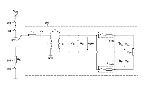
[0020] Figure 5 shows an equivalent circuit of an inductive link with series-
tuned
transmitter and parallel-tuned receiver resonant circuit according to one
embodiment of
the present invention.
[0021] Figure 6A-C shows state signals and voltage traces for various circuit
values in a
receiver resonant circuit.
Detailed Description of Specific Embodiments
[0022] An ASK-based signal transfer link system for data and energy
transmission as in
Fig. 2 has a potential problem. Assuming a periodic sequence of input states
RF-ON and
RF-OFF of voltage ui(t), and also assuming steady state conditions, dc-voltage
Vdc across
load Rd c is constant. During state RF-ON, voltage u2(t) reaches a peak
amplitude which is
slightly higher than Vdc/2. Switches 2031 or 2041 are closed if u2(t) > Vdc/2,
or if u2(t)
< -Vdc/2 respectively. Only during these very short periods charge is flowing
into the
network CA, CB, Rd. However, these diode currents define a particular loaded
quality
factor Q2,loaded, which is considerably smaller than the unloaded quality
factor Q2,unloaded as
defined in Equation (2) above.
[0023] If ui(t) changes from state RF-ON to RF-OFF, the voltage amplitude of
u2(t)
cannot immediately follow such a change. Instead, it will take some time for
the RF
amplitude to decrease back towards baseline, and the velocity of decay is
strongly
influenced by the quality factor of the receiver circuit: the lower the
quality factor, the
faster the decay is. Unfortunately, basically the unloaded quality factor 0
,2,unloaded which is
much higher than the loaded quality factor Q2,loaded applies here because as
soon as the
amplitude of u2(t) falls below Vdc/2, diode switches 2031 and 2041 remain
open, and no
RF energy can flow into the network CA, CB, R. During RF-OFF, the only
effective ac-
load within the receiver circuit is R2.
[0024] The exact relaxation behavior of u2(t) during RF-OFF is determined by
the network
R1, C1, L1, R2, C2, L2, and coupling factor k, and thus the unloaded quality
factors
-6-
CA 02676911 2009-07-29
WO 2008/101151 PCT/US2008/054065
Q 1,unloaded and Q2,unloaded are relevant. However, these quality factors
should be as high as
possible with respect to a high power transfer efficiency during RF-ON. So the
requirements for high power efficiency and fast RF-relaxation during RF-OFF in
an ASK
scheme are contradicting each other.
[0025] One way to address this problem is to decrease the quality factor in
the transmitter
resonant circuit during RF-OFF so that each rf data pulse will end with a more
rapid
decrease in pulse amplitude. One specific embodiment of a signal transfer link
is shown in
Fig. 5, which is a system for amplitude shift keying (ASK) transfer of rf data
pulses. Block
501 represents the inductive signal transfer link. Block 501 includes an
external series-
tuned resonant transmitter circuit for transmitting the rf data pulses using
ASK, and an
implanted parallel-tuned receiver module for receiving the rf data pulses. The
input node
502 is connected to a network composed of a switching pair 503 and 504,
resistor 505 and
switch 506. During state RF-ON, switch 506 is open (high impedance), and node
502 is
switched between ground potential and supply voltage VDD by means of switching
pair
503 and 504. This causes a rectangular voltage at radio frequency, and such an
operating
mode is usually designated as a class D switching paradigm. During state RF-
OFF,
switches 503 and 504 are open, and switch 506 is closed. Now RD series damping
resistor
505 is connected to R1 in series, which means a considerable reduction of the
transmitter
quality factor. This reduction of the quality factor for the transmitter
resonant circuit at the
end of each rf data pulse accelerates the decay of the RF amplitude in the
receiver resonant
circuit so as to minimize the time required for the trailing edge of the pulse
to rapidly
decrease back to baseline.
[0026] A quantitative analysis for the circuit in Fig. 5 has been carried out
with
specifications as summarized in Table 1. The simulations are based on a state
space model
with a computation time increment of 0.5 ns. The RF frequency is 10 MHz,
resulting in T
= 100 ns. Simulation results are shown in Fig. 6A-C where the upper traces
depict signal
state. For STATE = HIGH, the class D driver produces an RF-signal (state RF-
ON), and
for STATE = LOW, the input of the transmitter series circuit is connected to
RD (state RF-
-7-
CA 02676911 2009-07-29
WO 2008/101151 PCT/US2008/054065
OFF). Here, a self-clocking bit format with bit duration of 2 [is is assumed.
Note that the
shortest possible duration for RF-ON is 1 [Ls, which contains exactly 10 RF
cycles.
Table 1: Circuit Specifications
k 0.2
VDD 3 V
L1 2.70 i.tH
L2 0.85 i.tH
C1 82 pF
C2 260 pF
CA 10 nF
CB 10 nF
R1 2 SI
R2 2100 SI
Rdiode 40 SI
Rd c 10 kS2
Further simulations have been computed for different values of RD at a
coupling of k =
0.2. Figure 6A shows the result for RD = 0. Obviously, during periods STATE =
0, the
amplitude of u2(t) is decaying quite slowly and the decay is superimposed by a
typical beat
effect. Energy is oscillating between the transmitter and receiver resonant
circuits with a
beat frequency of about 2 MHz. Although the data structure can be identified
visually,
data detection by means of an electronic circuit cannot be easily achieved.
[0027] If the damping resistor is set to RD ¨> 00 as shown in Fig. 6B, the
beat effect
disappears. In this case, the receiver resonant circuit relaxes as if it was
not coupled to the
transmitter because the current in the transmitter is forced to zero. Thus the
behavior of a
2nd order system is observed, i.e., the amplitude of u2(t) decays
exponentially according to
the time constant of the unloaded receiver circuit L2, C2, R2. The waveform
u2(t) here is
less complex as compared to Fig. 6A. Note that the decay for RD ¨> 00 is
independent of
coupling factor k, which might be an important feature for subsequent data
decoding
-8-
CA 02676911 2009-07-29
WO 2008/101151 PCT/US2008/054065
stages. For example, in a cochlear implant system this is an important
criterion because the
data decoding should be insensitive the mutual coil positions.
[0028] Figure 6C shows the case for RD = 150 Q. Voltage u2(t) clearly
outperforms Figs.
6A and 6B, decaying comparatively fast at the end of each rf data pulse. Thus
u2(t) is very
well suited for data decoding.
[0029] One intrinsic advantage of embodiments such as the one shown in Fig. 5
is that
many components of the external system can be integrated onto a single
microchip, and
thus power consumption and system size can be kept very small. Also, an rf
generator (not
shown in Fig. 5) to drive switches 503 and 504 during RF-ON can easily be
integrated
onto such a microchip. The performance of switches 503 and 504 is of
particular
importance: the ON-resistances typically should not exceed 1 S2, and the gate
capacitances
should be smaller than 10 pF. However, such characteristics can be achieved
with existing
technologies such as, e.g., 0.35 ilm CMOS. In many signal transfer link
applications, it
may also be important that switches 503 and 504 are not closed simultaneously
during
RF-ON. Otherwise, very large currents can flow through the switches which
dramatically
enhance the power consumption and may damage circuit components.
[0030] Although various exemplary embodiments of the invention have been
disclosed, it
should be apparent to those skilled in the art that various changes and
modifications can be
made which will achieve some of the advantages of the invention without
departing from
the true scope of the invention.
-9-