Note: Descriptions are shown in the official language in which they were submitted.
CA 02676947 2009-07-29
DESCRIPTION
LED LIGHT SOURCE UNIT
TECHNICAL FIELD
The present invention relates to a light emitting diode (LED) light source
unit having a long life,
which employs a light emitting diode (LED) as a light source and which is
excellent in heat
dissipation performance.
BACKGROUND ART
In e.g. a liquid crystal display device comprising a liquid display element
and a backlight, it has
been common to use a small size fluorescent tube so-called CCFL (cold cathode
fluorescent lamp)
as a light source for the backlight.
The above CCFL (cold cathode fluorescent lamp) light source employs such a
structure that
mercury is sealed in a discharge tube so that ultraviolet rays emitted from
mercury excited by
discharge will hit a phosphor on a side wall of the cold cathode fluorescent
lamp and will be
converted to visible light. In consideration of an environmental aspect,
recently, it has been desired
to use a substitute light source which does not use hazardous mercury.
Recently, an LED light source unit using a light emitting diode (LED) as a
light source has
been used in various fields.
For example, as a new light source for liquid crystal display devices, one
using a light emitting
diode (hereinafter sometimes referred to simply as LED) has been proposed. LED
provides light
with directionality, and especially in a surface-mounted type such as one
mounted on e.g. a printed
board, light is taken out in one direction. Accordingly, as is different from
a conventional structure
employing CCFL (cold cathode fluorescent lamp), there is little loss of light,
and thus, it is used as a
backlight light source of a planar light source system (Patent Document 1).
Reflecting demands for lower price and improvement in luminous efficiency and
environment
regulations, a backlight using LED as a light source has started to be widely
used as a backlight for
liquid crystal display devices. At the same time, to meet demands for higher
luminance of liquid
crystal display devices and enlarging a display area, there has been a
progress in increasing the
number of LEDs mounted on a printed board and increasing the output in order
to improve the
amount of luminance.
However, with an LED light source, the luminous efficiency is not high, and
when LED emits
light, the majority of the input power will be discharged as a heat. When an
electric current is
applied, LED generates a heat and will be heated to a high temperature by the
generated heat. In
an extreme case, LED will be destroyed by such heat. Also in the case of a
backlight using LED as
a power source, such generated heat tends to be accumulated in LED and the
substrate on which
LED is mounted, and along with the increase of the temperature of LED, the
luminous efficiency of
LED itself tends to decrease. Besides, if it is attempted to increase the
number of LEDs to be
mounted or to increase the input power in order to increase the brightness of
the backlight, the
amount of such heat generation will increase, and it will be important to
further remove such heat.
In order to reduce the heat accumulation of an LED-mounted board and to reduce
the
temperature rise of an LED chip, a mounting metal film on which an LED chip is
to be mounted, a
driver wire to supply a driving current to the LED chip and a metal film-
pattern for the purpose of
heat dissipation, are formed on an LED chip-mounting face of an LED-mounted
board. Further, it
has been proposed that a metal film for heat dissipation is formed on a face
opposite to the LED
chip-mounting face, and in the thickness direction of the LED chip-mounted
board, a metal through-
hole is formed to connect a metal pattern on one main face side and a metal
film for heat dissipation
CA 02676947 2012-12-03
71416-412
2
on the other main face side, so that the heat generated from LED is released
to the rear side metal
film via the metal through-hole (Patent Document 2).
However, in such a case, the heat dissipation may be good to the rear side
metal film of the
printed board, but no heat dissipation from the housing located ahead of the
rear side metal film is
taken into consideration. Accordingly, in a case where LED is continuously
operated, there will be a
problem such that due to the temperature rise of LED, the luminous efficiency
of LED itself tends to
deteriorate. Further, there has been a problem that the printed board is
likely to get warped by an
influence of the heat generation from LED, whereby it tends to be peeled from
the adhesive tape, or
LED tends to be displaced from the desired position for emission of light,
whereby the desired optical
characteristics can not be obtained.
Further, a metal base circuit board having an insulating layer made of an
inorganic filler-filled
epoxy resin formed on a metal plate having a thickness of about 2 mm and
having a circuit pattern
formed thereon, is used as a circuit board for electronic equipments for
automobiles and
communication equipments having highly heat-generating electronic components
mounted thereon,
since it is excellent in heat dissipation performance and electric insulation
properties (Patent
Documents 3 and 4).
On the other hand, when a metal base circuit board employing a metal base
plate having a
thickness of about 2 mm is used instead of a printed board, it is possible to
obtain good heat
dissipation performance without providing metal through-holes or the like.
However, there are
problems such that the thickness of the board tends to be thick, and it is
required to take a larger
punching out size than the printed board in view of e.g. electrodes and wiring
patterns, whereby the
area of the board tends to be large. Further, it is not possible to optionally
bend a portion other than
the LED-mounted portion, whereby there will be a restriction with respect.to
e.g. the position where
an input terminal is to be formed.
Further, if it is attempted to reduce the thickness of the metal base plate of
the above metal
base circuit board to have a construction having the punching out size reduced
in the same manner
as a printed board in view of electrodes and the wiring pattern, there will be
a problem such that
since no consideration is given for heat dissipation from the housing located
ahead from the rear
side of the metal base plate, just like in the case of a printed board having
through-holes formed
=
therein, if LED is operated continuously, the luminous efficiency of LED
itself tends to deteriorate
along with the temperature rise of LED. Further, there has been a problem such
that even when
the metal base circuit board deforms only a little, cracks are likely to form
in the insulating layer to a
practically unacceptable level, and the LED-mounted portion can not be freely
bent.
Patent Document 1: JP-A-2005-293925
Patent Document 2: JP-A-2005-283852
Patent Document 3: JP-A-62-271442
Patent Document 4: JP-A-06-350212
CA 02676947 2012-12-03
71416-412
3
DISCLOSURE OF THE INVENTION
According to an aspect of the present invention, there is provided an LED
light source unit comprising a printed board, at least one light emitting
diode provided on
the printed board, and an adhesive tape for fixing the printed board on the
surface of a
heat dissipating member, wherein the thermal conductivity of the adhesive tape
is from 1
to 4 W/mK, and the withstand voltage between a fixing face of the printed
board and a
fixing face of the heat dissipating member is at least 1.0 kV, wherein the
printed board is
a board having a conductor circuit provided on a metal base plate via an
insulating layer
comprising an inorganic filler and an epoxy resin and having a thermal
conductivity of
from 1 to 4 W/mK, wherein the thickness of the metal base plate is from 100 to
500 pm,
the thickness of the insulating layer is from 20 to 300 pm, and the thickness
of the
conductor circuit is from 9 to 140 pm.
Some embodiments may improve the heat dissipation performance while
maintaining the thickness of an LED-mounted board having an LED power source
mounted thereon to be as thin as the conventional level and maintaining the
width of the
board to be narrow and yet without necessity to form through-holes immediately
below
LED or to pattern the metal film for heat dissipation on the LED-mounted
surface on the
mounted-board, and consequently may provide an LED light source unit which is
bright
and has a long life and which is free from a damage of LED.
Another aspect may provide:
(1) An LED light source unit comprising a printed board, at least one light
emitting diode provided on the printed board, and an adhesive tape for fixing
the printed
board on the surface of a heat dissipating member, wherein the thermal
conductivity of
the adhesive tape is from 1 to 4 W/mK, and the withstand voltage between a
rear side
conductor circuit and a metal housing is at least 1.0 kV.
Some embodiments may provide:
(2) The LED light source unit according to the above (1), wherein the
thickness of the adhesive tape is from 30 to 300 pm.
CA 02676947 2012-12-03
=
71416-412
4
(3) The LED light source unit according to the above (1), wherein the
thickness of the
adhesive tape is from 30 to 50 pm.
(4) The LED light source unit according to any one of the above (1) to (3),
wherein the
adhesive tape comprises from 20 to 45 vol% of a polymer resin material made of
a copolymer of
(meth)acrylic acid with a monomer copolymerizable with (meth)acrylic acid, and
from 40 to 80 vol%
of an inorganic filler having a particle size of at most 45 pm and an average
particle size of from 0.3
to 30 pm.
(5) The LED light source unit according to the above (4), wherein the
inorganic filler is at least
one member selected from the group consisting of aluminum oxide, aluminum
nitride, boron nitride,
silicon oxide (silica) and aluminum hydroxide.
(6) The LED light source unit according to any one of the above (1) to (5),
wherein the
adhesive tape contains glass cloth.
(7) The LED light source unit according to the above (1), wherein the adhesive
tape comprises
a silicone rubber sheet having a thermal conductivity of from 2 to 5 W/mK and
an adhesive layer
containing (meth)acrylic acid, formed on each side of the silicone rubber
sheet, wherein the
thickness of the silicone rubber sheet is from 100 to 300 pm, and the
thickness of the adhesive layer
formed on each side is from 5 to 40 pm.
(8) The LED light source unit according to any one of the above (1) to (7),
wherein the
adhesive strength between the adhesive tape and the fixing face of the printed
board and the
adhesive strength between the adhesive tape and the fixing face of the heat
dissipating member, are
from 2 to 10 N/cm.
(9) The LED light source unit according to any one of the above (1) to (8),
wherein the printed
board is a printed board comprising an insulating layer made of a composite
material (prepreg)
having a glass cloth base material impregnated with an epoxy resin, and a
copper foil bonded to
each side of the insulating layer, wherein a prescribed circuit pattern is
formed on the copper foil,
and through-holes are formed immediately below said LED mounted.
(10) The LED light source unit according to the above (9), wherein a plated
conductor or a
conductor is embedded in the through-holes.
(11) The LED light source unit according to any one of the above (1) to (8),
wherein the
printed board is a board having a conductor circuit provided on a metal base
plate via an insulating
layer comprising a thermoplastic resin or a thermosetting resin and having a
thermal conductivity of
from 1 to 4 W/mK, wherein the thickness of the metal base plate is from 100 to
500 pm, the
thickness of the insulating layer is from 20 to 300 pm, and the thickness of
the conductor circuit is
from 9 to 140 Lim.
(12) The LED light source unit according to the above (11), wherein the
insulating layer
comprises from 25 to 50 vol% of a thermoplastic resin or a thermosetting
resin, and the rest being an
inorganic filler which has a particle size of at most 100 pm and comprises
coarse particles having an
average particle size of from 10 to 40 pm and fine particles having an average
particle size of from
0.4 to 1.2 pm and which has a sodium ion concentration of at most 500 ppm.
CA 02676947 2012-12-03
71416-412
4a
(13) The LED light source unit according to the above (11) or (12), wherein
the chloride ion
concentration in the thermoplastic resin or the thermosetting resin is at most
500 ppm.
(14) The LED light source unit according to any one of the above (11) to (13),
wherein the
thermoplastic resin is at least one fluororesin selected from the group
consisting of a
tetrafluoroethylene/perfluoroalkoxyethylene copolymer, a
tetrafluoroethylene/hexafluoropropylene
copolymer and a chlorotrifluoroethylene/ethylene copolymer.
(15) The LED light source unit according to any one of the above (11) to (13),
wherein the
thermosetting resin is at least one member selected from the group consisting
of an epoxy resin, a
phenol resin, a silicone resin and an acrylic resin.
(16) The LED light source unit according to any one of the above (11) to (13),
wherein the
thermosetting resin is a bisphenol A or bisphenol F epoxy resin, or a
hydrogenated bisphenol A or
bisphenol F epoxy resin.
(17) The LED light source unit according to any one of the above (11) to (13),
wherein the
thermosetting resin is a bisphenol A or bisphenol F epoxy resin, and contains
a novolac resin as an
epoxy-curing agent.
(18) The LED light source unit according to any one of the above (11) to (13),
wherein the
thermosetting resin is a hydrogenated bisphenol F or A epoxy resin and further
contains a linear high
molecular weight epoxy resin having an epoxy equivalent of from 800 to 4,000.
According to some embodiments, it is possible to effectively dissipate heat
generated from
an LED light source from the rear side of a printed board to a metal housing
via an adhesive tape
having electrical insulating properties and thermal conductivity.
Specifically, even when a printed
board having a circuit formed on each side is used, by securing electrical
insulating properties and
thermal conductivity by an adhesive tape having electrical insulating
properties and thermal
conductivity, it becomes possible to dissipate the heat to the exterior via
the adhesive tape without
necessity to protect with a coverlay film (such as a polyimide film) the
circuit surface on the side to
be fixed to the metal housing. Accordingly, it is possible to obtain effects
to reduce heat
accumulation on the LED-mounted board and to reduce the temperature rise of
LED. It is thereby
possible to provide an LED light source unit which is bright and has a long
life and which is capable
of suppressing the decrease in luminous efficiency of LED and able to prevent
a damage to LED.
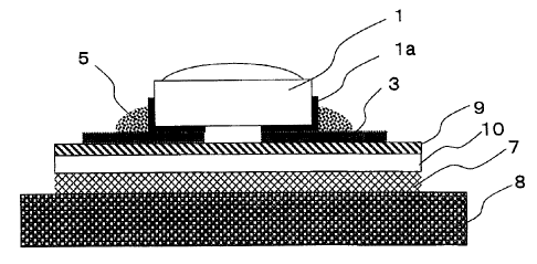
BRIEF DESCRIPTION OF THE DRAWINGS
Fig. 1 is a cross-sectional view illustrating an embodiment of the LED light
source unit
according to the present invention.
Fig. 2 is a cross-sectional view illustrating another embodiment of the LED
light source unit
according to the present invention.
1: LED
la: LED electrode terminal
2: Base material
3: Conductor circuit
4: Rear side conductor circuit (lead wire)
5: Solder connection
6: Via hole (through-hole)
7: Adhesive tape
8: Housing
9: Thermally conductive insulating layer
10: Metal base plate
CA 02676947 2009-07-29
BEST MODE FOR CARRYING OUT THE INVENTION
Fig. 1 is a cross-sectional view schematically illustrating the structure of
one embodiment of
the LED light source unit of the present invention.
5 The LED light source unit of the present invention has a printed board
comprising a base
material 2, a conductor circuit 3 and a rear side conductor circuit 4, wherein
at least one LED 1 is
mounted on the conductor circuit 3, as bonded by e.g. a solder connection 5,
and is closely adhered
to a housing 8 made of e.g. aluminum having heat dissipating properties via a
thermally conductive
adhesive tape 7 having electrical insulating properties. The conductor circuit
3 and the rear side
conductor circuit 4 are electrically connected by via holes (or through-holes)
6, so that an electric
power can be input to LED 1 from outside.
In Fig. 1, the printed board is, for example, one comprising an insulating
layer made of a
composite material (prepreg) having a glass cloth base material impregnated
with an epoxy resin,
and a copper foil bonded to each side of the insulating layer. On the above
copper foil of the
printed circuit, a prescribed circuit pattern is formed, and via holes 6
(through-holes) are formed
immediately below the LED mounted.
The via holes 6 formed immediately below the LED mounted have a role of
transmitting heat
from LED to the rear side of the metal base material, and they are certainly
required in a case where
a printed board is employed which has an insulating layer made of a composite
material (prepreg)
having a glass cloth base material impregnated with an epoxy resin, and which
has a copper foil
bonded on each side of the insulating layer. It is particularly effective that
the via holes 6 are
formed by cylindrical copper for the purpose of increasing the heat
dissipation performance.
The thermally conductive adhesive tape 7 is one having the thermal
conductivity improved
over conventional adhesive tapes in order to efficiently dissipate the heat
generated during the light
emission of LED from the rear side of the metal base material to the housing
via the metal base
material. With an adhesive tape having no thermal conductivity, the thermal
conductivity of the heat
generated at the time of light emission of LED to the housing tends to be
inadequate, thus leading to
an increase of the temperature of LED, such being practically not useful.
The thermally conductive adhesive tape to be used in the present invention has
a thermal
conductivity of from 1 to 4 W/mK, preferably from 3 to 4 W/mK, and the
thickness of the adhesive
tape is from 30 to 300 pm, preferably from 30 to 150 pm, more preferably from
30 to 50 pm.
The thermally conductive adhesive tape 7 to be used in the present invention
is preferably one
having a thermally conductive electrically insulating agent filled in a
polymer resin material, as will be
described hereinafter.
The polymer resin material to be used for the thermally conductive adhesive
tape 7 of the
present invention is not particularly limited. However, in order to improve
the adhesion to metal, a
polymer resin material is preferably selected which is made of a copolymer of
acrylic acid and/or
methacrylic acid (hereinafter referred to also as (meth)acrylic acid) and a
monomer copolymerizable
with such (meth)acrylic acid.
The above monomer copolymerizable with (meth)acrylic acid is preferably an
acrylate or
methacrylate having a C2_12 alkyl group. From the viewpoint of the flexibility
and processability, a
preferred monomer may, for example, be one or more selected from ethyl
acrylate, propyl acrylate,
butyl acrylate, 2-ethyhexyl acrylate, octyl acrylate, isooctyl acrylate, decyl
acrylate, decyl
methacrylate and dodecyl methacrylate. Among them, a copolymer of a monomer
containing a
(meth)acrylic acid ester monomer is further preferred. As such a monomer, 2-
ethylhexyl acrylate is
particularly preferred.
The thermally conductive electrically insulating agent to be incorporated in
the thermally
conductive adhesive tape 7, is preferably contained in an amount of from 40 to
80 vol%, more
CA 02676947 2009-07-29
6
preferably from 50 to 70 vol%, in the thermally conductive adhesive tape 7,
since it is thereby
possible to secure good heat dissipation performance. As such a thermally
conductive electrically
insulating agent, various inorganic fillers or organic fillers, which are
excellent in electrical insulating
properties and thermal conductivity, may be used.
An inorganic filler may, for example, be a metal oxide such as aluminum oxide
(alumina),
silicon oxide (silica) or titanium dioxide, a nitride such as aluminum
nitride, boron nitride or silicon
nitride, silicon carbide, or aluminum hydroxide. Among them, it is preferably
at least one member
selected from the group consisting of alumina, crystalline silica and aluminum
hydroxide. Further, it
is also possible to select one having the surface treated with e.g. a silane
coupling agent. With
respect to the particle size of the inorganic filler, the particle size is
preferably at most 45 pm,
particularly preferably from 20 to 40 pm, and the average particle size is
preferably from 0.3 to 30
pm, particularly preferably from 10 to 20 pm, from the viewpoint of the
thickness of the adhesive tape
and the filling property.
As an organic filler, a rubber such as natural rubber, acrylic rubber,
nitrile/butadiene rubber
(NBR) or ethylenepropylenediene rubber (EPDM) is preferred. It is particularly
preferred to contain
acrylic rubber.
The acrylic rubber is preferably one made of a polymer of an acrylate or
methacrylate having
a C2-12 alkyl group from the viewpoint of the flexibility and adhesive
properties. For example, it may
be a polymer of one monomer selected from ethyl acrylate, n-propyl acrylate, n-
butyl acrylate,
isobutyl acrylate, n-pentyl acrylate, isoamyl acrylate, n-hexyl acrylate, 2-
methylpentyl acrylate, n-
dodecyl acrylate, n-octadecyl acrylate, cyanomethyl acrylate, 1-cyanoethyl
acrylate, 2-cyanoethyl
acrylate, 1-aminopropyl acrylate and 2-cyanopropyl acrylate, or a polymer of a
monomer mixture
having at least two types of such monomers blended. Among them, a preferred
monomer is 2-
ethylhexyl acrylate.
By incorporating glass cloth to the thermally conductive adhesive tape 7, it
is possible to
remarkably improve the electrical insulating properties as well as the
mechanical strength of the
adhesive tape. The glass cloth is extremely effective since it not only
provides the effect as a
reinforcing material for the thermally conductive adhesive tape but also has
an effect as a reinforcing
material for an adhesive tape for bonding the housing and the printed board
and is capable of
preventing electrical short circuit which may otherwise occur when the bonding
pressure to bond the
housing and the printed board is so strong that the distance between the
housing and the rear side
of the printed board becomes too close. Namely, even if the bonding pressure
at the time of
bonding the housing and the printed board is too strong, the housing and the
rear side of the printed
board could not be closer than the thickness of the glass cloth, whereby the
electrical characteristics
can be secured.
As such glass cloth, glass fiber excellent in quality and cost produced by a
direct melting
method of spinning it directly from a melting furnace, is preferably employed.
With respect to the
composition of such glass fiber, preferred is one obtained by processing E
glass (alumina/calcium
borosilicate glass) as alkali free glass to be used for electrical
applications, into long fiber. The
glass cloth is preferably an electrically insulating non-woven fabric such as
a wet system non-woven
fabric of e.g. glass. The thickness of the glass cloth is preferably from 10
pm to 200 pm, more
preferably from 20 pm to 50 pm. Further, in a case where glass cloth of glass
long fiber made of
alumina/calcium borosilicate glass is to be used, the electrical insulation
reliability of the thermally
conductive adhesive tape will be further improved, whereby the reliability of
the LED light source unit
will further be improved.
The thermally conductive adhesive tape 7 may contain a known polymer resin
composition
within a range not to impair the desired characteristics of the present
invention. Further, at the time
of curing the thermally conductive adhesive tape 7, an additive to control the
viscosity or an additive
CA 02676947 2009-07-29
7
such as a modifier, an aging-preventive agent, a heat stabilizer or a
colorant, may be incorporated
as the case requires, within a range not to present an adverse effect.
The thermally conductive adhesive tape 7 can be cured by a usual method. For
example, it
may be cured by a method such as thermal polymerization by means of a thermal
polymerization
initiator, photopolymerization by means of a photopolymerization initiator or
polymerization by means
of a thermal polymerization initiator and a curing accelerator. Among them,
photopolymerization by
means of a photopolymerization initiator is preferred from the viewpoint of
the productivity, etc.
As specific forms of the thermally conductive adhesive tape 7, various types
may be
mentioned. For example, a thermally conductive adhesive tape may be mentioned
which has an
adhesive layer containing (meth)acrylic acid on each side of a silicon rubber
sheet containing boron
nitride particles and having a thermal conductivity of from 2 to 5 W/mK,
wherein the thickness of the
silicon rubber sheet is from 100 pm to 300 pm, and the thickness of the
adhesive layer formed on
each side is from 5 pm to 40 pm.
In the LED light source unit of the present invention, the adhesive strength
between the
thermally conductive adhesive tape 7 and the housing 8 as a heat dissipating
member is preferably
from 2 to 10 N/cm, more preferably from 4 to 8 N/cm. If the adhesive strength
is lower than the
above range, the adhesive tape tends to be easily peeled from the fixing face
of the printed board or
from the fixing face of the heat dissipating member. On the other hand, if the
adhesive strength is
higher than the above range, there will be a problem in handling efficiency,
whereby the productivity
may sometimes decrease, such being undesirable.
In the LED light source unit of the present invention, the withstand voltage
between the rear
side conductor circuit and the metal housing (i.e. the withstand voltage
between the fixing face of the
printed board and the fixing face of the heat dissipating member) is at least
1.0 V, preferably at least
1.5 V. When such withstand voltage is at least 1.0 V, insulation between the
board and the metal
housing can be attained. There is no upper limit for such withstand voltage,
and the higher the
withstand voltage, the better.
Fig. 2 is a cross-sectional view schematically illustrating the construction
of another
embodiment of the LED light source unit of the present invention having an
insulating layer.
In the LED light source unit in Fig. 2, on a conductor circuit 3 of a printed
board comprising the
conductor circuit 3, an insulating layer 9 having thermal conductivity and a
metal base plate 10, at
least one LED 1 is mounted as bonded by e.g. solder and closely bonded to a
housing 8 having heat
dissipation properties via a thermally conductive adhesive tape 7.
In the LED light source unit in Fig. 2, the insulating layer 9 of the printed
board having the
metal base plate 10 has thermal conductivity, whereby heat generated from LED
1 is transferred to
the metal base plate 10 via the insulating layer 9 and can be dissipated to
the housing 8 having heat
dissipating properties via the adhesive tape 7 having thermal conductivity.
Therefore, it is possible
to efficiently dissipate the heat generated from LED 1 to the housing 8
without providing via holes
(through-holes) in the printed board as in Fig. 1.
Further, the printed board has the metal base plate 10, whereby even when the
LED light
source unit is continuously operated for more than 3,000 hours, the printed
board will not be warped
by the heat generation of LED, and there will be no such a problem that the
adhesive tape peels or
LED is displaced from the desired position to deteriorate the essential
optical properties.
In the LED light source unit in Fig. 2, the thickness of the metal base plate
10 is from 100 to
500 pm, and the insulating layer 9 contains an inorganic filler and a
thermoplastic resin or
thermosetting resin and has a thickness of preferably from 20 to 300 pm,
particularly preferably from
80 to 150 pm, and the thickness of the above conductor circuit is preferably
from 9 to 140 pm,
particularly preferably from 18 to 70 pm. With respect to the thickness of the
insulating layer 9, if it
is less than 20 pm, the insulating performance tends to be low, and if it
exceeds 300 pm, the heat
CA 02676947 2009-07-29
8
dissipation performance tends to be low.
As the metal base plate 10, it is possible to use copper or a copper alloy, an
aluminum alloy,
iron, stainless steel, having good thermal conductivity. The thickness of the
metal base plate 10 is
selected from a range of from 100 pm to 500 pm, preferably from 150 to 300 pm.
If the thickness of
__ the metal base plate 10 is less than 100 pm, the rigidity of the circuit
board based on the metal base
plate tends to be low, and its application tends to be limited, and it tends
to be difficult to suppress
warpage of the printed board when LED is continuously operated. If the
thickness of the metal
base plate 10 exceeds 500 pm, the thickness of the LED light source unit tends
to be thick, such
being undesirable.
The insulating layer 9 contains a thermoplastic resin and/or thermosetting
resin in an amount
of preferably from 25 to 50 vol%, more preferably from 30 to 45 vol%, and the
rest being an
inorganic filler.
The thermoplastic resin to be contained in the insulating layer 9 is
preferably a heat resistant
resin, and it is particularly preferred to use a fluororesin which may be heat-
melted to be combined
__ with an inorganic filler. Specifically, the fluororesin is at least one
member selected from the group
consisting of a tetrafluoroethylene/perfluoroalkoxyethylene copolymer, a
tetrafluoroethylene/hexafluoropropylene copolymer and a
chlorotrifluoroethylene/ethylene
copolymer.
As the thermosetting resin to be contained in the insulating layer 9, an epoxy
resin, a phenol
__ resin, a silicone resin or an acrylic resin may, for example, be used.
Among them, an epoxy resin is
preferred, since such will be excellent in the adhesive strength with the
metal base plate 10 and the
conductor circuit 3 in the cured state while containing the inorganic filler,
and it is excellent in heat
resistance.
As a curing agent for the epoxy resin, any curing agent may be used without
any particular
__ restriction so long as it is capable of curing the above epoxy resin.
However, a compound having a
hydroxyl group is preferred from the viewpoint of the electrical
characteristics of the obtainable cured
product. As a specific example, it is possible to employ at least one member
selected from the
group consisting of an amine curing agent, an acid anhydride curing agent, a
phenol curing agent
and a dicyanannide. Particularly in consideration of the productivity and
adhesion property,
__ preferred is a phenol resin represented by a phenol novolac resin or a
bisphenol A novolac resin
having a softening point of at most 130 C. Further, in order to secure the
rigidity, insulating
property, etc. of the insulating layer, it is preferred to add such a resin so
that the hydroxyl group
equivalent will be preferably from 0.7 to 1.1 times, more preferably from 0.8
to 1.0 time, to the epoxy
equivalent of the epoxy resin contained in the thermosetting resin.
The above epoxy resin is preferably a bisphenol A or bisphenol F epoxy resin.
One having
an epoxy equivalent of preferably at most 240, more preferably from 180 to
220, is suitable, since it
is liquid at room temperature. Particularly, it is preferred to use a
hydrogenated bisphenol A or
bisphenol F epoxy resin, in order to improve the flexibility of the
thermosetting resin after curing.
The hydrogenated bisphenol A or bisphenol F epoxy resin has a low viscosity,
whereby it
__ becomes possible to incorporate a linear high molecular weight epoxy resin
having an epoxy
equivalent of preferably from 800 to 4,000, particularly preferably from 1,000
to 2,000 to the
thermosetting resin in a large amount at the maximum of 40 mass%, or to
incorporate an inorganic
filler in the insulating layer in an amount of as much as from 50 to 75 vol%.
It is preferred to incorporate the above linear high molecular weight epoxy
resin having an
__ epoxy equivalent of from 800 to 4,000, preferably from 1,000 to 2,000 to
the insulating layer 9,
whereby the bonding property will be improved, and the flexibility at room
temperature will be
improved. The content of such a linear high molecular weight epoxy resin is
preferably at most 40
mass%, more preferably at most 30 mass% in the thermosetting resin. If it
exceeds 40 mass%, the
CA 02676947 2009-07-29
9
amount of the curing agent for the epoxy resin relatively decreases, whereby
the glass transition
temperature (Tg) of the thermosetting resin may be increased, and the
flexibility may sometimes be
decreased.
As the thermosetting resin constituting the insulating layer 9, a phenol
resin, a polyimide resin,
a phenoxy resin, an acrylic rubber, an acrylonitrile/butadiene rubber, etc.
may be incorporated to the
resin composed mainly of the above epoxy resin. Their amount is at most 30
mass%, preferably at
most 20 mass%, based on the total amount with the epoxy resin, in
consideration of the electrical
insulating property, and thermal resistance, etc.
The thermoplastic resin constituting the insulating layer 9 may, for example,
be polyethylene,
polypropylene, polystyrene or a fluororesin. Among them, a fluororesin is
preferred since, in
addition to its characteristics that it is excellent in the thermal
resistance, chemical resistance and
weather resistance, it is excellent in the electrical insulating properties,
and further, in its molten
state, a thermally conductive filler can readily be dispersed therein.
The chloride ion concentration in the thermoplastic resin or thermosetting
resin constituting
the insulating layer 9 is preferably at most 500 ppm, more preferably at most
250 ppm. In the prior
art, if the chloride ion concentration in the thermoplastic resin or the
thermosetting resin composition
is at most 1,000 ppm, the electrical insulating properties were good even at a
high temperature
under a DC voltage.
However, the thermoplastic resin or the thermosetting resin constituting the
insulating layer 9
in the present invention has a flexible structure such that it can be bent
even at room temperature,
and therefore, if the chloride ion concentration exceeds 500 ppm, transfer of
ionic impurities is likely
to take place at a high temperature under a DC voltage, whereby the electrical
insulating properties
may tend to deteriorate. When the chloride ion concentration is low, it is
possible to obtain an LED
light source unit which is reliable over a long period of time.
The inorganic filler to be incorporated in the insulating layer 9 is
preferably one having
electrical insulating properties and is excellent in thermal conductivity. For
example, silicon oxide
(silica), preferably crystalline silica, alumina, aluminum nitride, silicon
nitride or boron nitride may be
used. The content of the inorganic filler in the insulating layer 9 is
preferably from 50 to 75 vor/o,
more preferably from 55 to 70 vor/o.
As the inorganic filler, preferred is one comprising coarse particles having a
particle size of at
most 100 pm and an average particle size of from 10 to 40 pm, preferably from
15 to 25 urn, and fine
particles having an average particle size of from 0.4 to 1.2 pm, preferably
from 0.6 to 1.1 urn.
When such coarse particles and fine particles are mixed, higher packing will
be possible, over a case
where coarse particles or fine particles are used alone.
The sodium ion concentration in the inorganic filler is preferably at most 500
ppm, more
preferably at most 100 ppm. If the sodium ion concentration in the inorganic
filler exceeds 500
ppm, transfer of ionic impurities is likely to take place at a high
temperature under a DC voltage,
whereby the electrical insulating properties may tend to deteriorate.
The LED light source unit in Fig. 2 has the above-described construction, and
the above-
mentioned insulating layer comprises an inorganic filler and a thermosetting
resin or thermoplastic
resin and has a thickness of from 20 to 300 pm, preferably from 50 to 200 pm.
The thickness of the
conductor circuit is from 9 to 140 pm, preferably from 18 to 70 urn. Further,
the thickness of the
metal base plate is from 100 to 500 urn, preferably from 10 to 300 pm, the
thickness of the above
conductor circuit is from 9 to 140 pm, preferably from 18 to 70 pm, and the
thermoplastic resin
constituting the insulating layer contains a fluororesin.
As a preferred embodiment of the above insulating layer, one having a thermal
conductivity of
from 1 to 4 W/mK is used. Therefore, the LED light source unit of the present
invention has high
heat dissipation performance and withstand voltage characteristics as compared
with an LED light
CA 02676947 2009-07-29
source unit employing a conventional printed board, such that the withstand
voltage between the
conductor circuit and the metal foil is at least 1.5 kV. Accordingly, it is
possible to efficiently
dissipate the heat generated from the LED light source to the rear side of the
board and further to
the exterior, whereby heat accumulation in the LED-mounted board will be
reduced, and the
5 temperature rise may be reduced, and thus it is possible to suppress a
decrease in the luminous
efficiency of LED and thus prevent a damage to LED, and LED will be bright and
have a long life.
When flexibility is required for the board, the glass transition temperature
of the insulating
layer is from 0 to 40 C. If the glass transition temperature is lower than 0
C, the rigidity and
electrical insulating properties tend to be low, and if it exceeds 40 C, the
flexibility tends to decrease.
10 When the glass transition temperature is from 0 to 40 C, decrease of the
withstand voltage due to
peeling between the metal base plate 10 and the insulating layer 9 or due to
cracking of the
insulating layer, tends to hardly take place even if bend processing or
drawing processing is carried
out at room temperature, as is different from one which is hard at room
temperature like an
insulating layer used in a conventional metal base substrate.
EXAMPLES
Now, the present invention will be described in further detail with reference
to Examples and
Comparative Examples. However, it should be understood that the present
invention is by no
means thereby restricted.
EXAMPLE 1
An LED light source unit of the type shown in Fig. 1 was prepared. Namely,
with a glass
cloth-incorporated printed board having a copper foil with a thickness of 35
pm formed on each side
of an epoxy resin cloth impregnated with a glass base material with a
thickness of 100 pm, through-
holes were formed at predetermined positions (positions to connect a conductor
circuit connected to
an electrode terminal la of LED and a rear side conductor circuit located
immediately therebelow)
and copper-plated, and then, a conductor circuit on which LED is to be
mounted, and a rear side
conductor circuit to dissipate heat and to light up LED, were formed to obtain
a printed board.
To 90 mass% of 2-ethylhexyl acrylate ("2EHA", manufactured by TOAGOSEI CO.,
LTD.)
having 10 mass% of acrylic rubber ("AR-53L", manufactured by ZEON CORPORATION)
dissolved
therein, 10 mass% of acrylic acid ("AA", manufactured by TOAGOSEI CO., LTD.)
was mixed. To
the mixture, 0.5 mass% of a photopolymerization initiator 2,2-dimethoxy-1,2-
diphenylethan-1-one
(manufactured by Ciba Specialty Chemicals), 0.2 mass% of triethylene glycol
dimercaptan
(manufactured by Maruzen Chemical) and 0.2 mass% of 2-butyl-2-ethyl-1,3-
propanediol diacrylate
(manufactured by KYOEISHA CHEMICAL CO., LTD.) were further added and mixed to
obtain a resin
composition A.
Further, 80 mass% of a hydrogenated bisphenol A-type epoxy resin ("EXA-7015",
manufactured by Dainippon Ink and Chemicals Incorporated) and 20 mass% of an
aromatic
polyamine ("H-84B" manufactured by Nippon Synthetic Chemical Industry Co.,
Ltd.) were mixed to
obtain a resin composition B.
Then, 45 vol% of the resin composition A, 15 vol% of the resin composition B
and 40 vol% of
aluminum oxide having a particle size of at most 65 pm and an average particle
size of 20 pm
("DAW-20", manufactured by Denki Kagaku Kogyo Kabushiki Kaisha) as an
inorganic filler were
mixed and dispersed to obtain a resin composition C.
The resin composition C subjected to defoaming treatment was applied on a PET
(polyethylene terephthalate) film having a thickness of 75 pm and having
release treatment applied
on its surface, and a PET film having release treatment applied on its surface
was further covered
thereon, whereupon ultraviolet rays with a wavelength of 365 nm were applied
from both sides with a
dose of 3,000 mJ/cm2. Thereafter, heat treatment was carried out at 100 C for
3 hours to cure the
CA 02676947 2009-07-29
11
resin composition C thereby to obtain a thermally conductive adhesive tape
having electrical
insulating properties.
Then, cream solder (M705, manufactured by Senju Metal Industry Co., Ltd.) was
applied by
metal mask (screen printing) at a predetermined position of a conductor
circuit of a printed board,
and LED (NFSW036B, manufactured by Nichia Corporation) was mounted by means of
a solder-
ref low apparatus. Then, the thermally conductive adhesive tape having
electrical insulating
properties was bonded to the side of the printed board having no LED mounted,
and fixed to a metal
housing to obtain an LED light source unit.
With respect to the obtained LED light source unit, (1) the initial withstand
voltage between the
rear side conductor circuit and the metal housing, (2) the withstand voltage
between the rear side
conductor circuit and the metal housing after being left at a high temperature
under high humidity, (3)
the adhesive strength between the adhesive tape and the fixing face of the
printed board, (4) the
adhesive strength between the adhesive tape and the fixing face of the printed
board after being left
at high temperature under high humidity, (5) the adhesive strength between the
adhesive tape and
the fixing face of the heat dissipating member, (6) the adhesive strength
between the fixing face of
the printed board and the fixing face of the heat dissipating member after
being left at high
temperature under high humidity, (7) the thermal conductivity of the thermally
conductive adhesive
tape, (8) the initial LED lighting-up, (9) LED lighting-up after being left at
high temperature under high
humidity, and (10) the warpage of the board after continuous lighting-up, etc.
were measured by the
following methods. The obtained results are shown in Table 1.
(1) Initial withstand voltage between the rear side conductor circuit and the
metal housing
The withstand voltage between the rear side conductor circuit of the printed
board and the
metal housing was measured by a stepwise pressure-raising method stipulated by
JIS C2110 in an
environment at a temperature of 23 C with a humidity of 30%.
(2) Withstand voltage between the rear side conductor circuit and the metal
housing after
being left at high temperature under high humidity
After being left for 1,000 hours in an environment at a temperature of 85 C
with a humidity of
85%, the withstand voltage between the rear side conductor circuit of the
printed board and the
metal housing was measured by a stepwise pressure-raising method stipulated in
JIS C2110 in an
environment at a temperature of 23 C with a humidity of 30%.
(3) Adhesive strength between the adhesive tape and the fixing face of the
printed board
The adhesive strength between the adhesive tape and the printed board was
measured by
peeling the adhesive tape by a method stipulated in JIS C6481 in an
environment at a temperature
of 23 C with a humidity of 30%.
(4) Adhesive strength between the adhesive tape and the fixing face of the
printed board after
being left at high temperature under high humidity
After being left for 1,000 hours in an environment at a temperature of 85 C
with a humidity of
85%, the adhesive strength between the adhesive tape and the printed board was
measured by
peeling the adhesive tape by a method stipulated in JIS C6481 in an
environment at a temperature
of 23 C with a humidity of 30%.
(5) Adhesive strength between the adhesive tape and the fixing face of the
heat dissipating
member
The adhesive strength between the adhesive tape and the fixing face of the
heat dissipating
member (aluminum housing) was measured by peeling the adhesive tape by a
method stipulated in
JIS C6481 in an environment at a temperature of 23 C with a humidity of 30%.
(6) Adhesive strength between the fixing face of the printed board and the
fixing face of the
heat dissipating member after being left at high temperature under high
humidity
After being left for 1,000 hours in an environment at a temperature of 85 C
with a humidity of
CA 02676947 2009-07-29
12
85%, the adhesive strength between the adhesive tape and the fixing face of
the heat dissipating
member (aluminum housing) was measured by peeling the adhesive tape by a
method stipulated in
JIS C6481 in an environment at a temperature of 23 C with a humidity of 30%.
(7) Thermal conductivity of thermally conductive adhesive tape
The test sample was laminated so that the thickness would be 10 mm and
processed into 50
mm x 10 mm, whereupon the thermal conductivity was obtained by a quick thermal
conductivity
meter (QTM-500, manufactured by Kyoto Electronics Industry Co., Ltd.).
(8) Initial LED lighting-up test
In an environment at a temperature of 23 C with a humidity of 30%, a rated
current of 450 mA
was applied to LED to light up LED, and upon expiration of 15 minutes, the
temperature at the solder
connection portion of LED was measured.
(9) LED lighting-up test after being left at high temperature under high
humidity
A LED light source unit was left for 1,000 hours in an environment at a
temperature of 85 C
with a humidity of 85%, and again, a rated current of 450 mA was applied to
LED in an environment
at a temperature of 23 C with a humidity of 30% to light up LED. Upon
expiration of 15 minutes,
the temperature of the solder connection portion of LED was measured.
(10) Warpage of the board after continuous lighting-up
With respect to an LED light source unit, in an environment at a temperature
of 23 C with a
humidity of 30%, a current of 150 mA was applied to LED for 3,000 hours to
continuously light up
LED, whereupon warpage of the board (the position at 5 mm from the LED-mounted
portion) was
measured by means of a micrometer.
EXAMPLE 2
An LED light source unit was prepared in the same manner as in Example 1
except for the
following. Namely, as an inorganic filler, aluminum oxide ("DAW-10",
manufactured by Denki
Kagaku Kogyo Kabushiki Kaisha) was classified by a sieve of 45 pm to obtain an
inorganic filler A
having a maximum particle size of at most 45 pm and an average particle size
of 9 pm. And, 40
vol% of the inorganic filler A, 45 vol% of the resin composition A and 15 vol%
of the resin
composition B were mixed to obtain a resin composition D.
Then, the resin composition D subjected to defoaming treatment was applied on
a PET film
having a thickness of 75 pm and having release treatment applied to its
surface, and further, a PET
film having release treatment applied to its surface was covered thereon,
whereupon ultraviolet rays
with a wavelength of 365 nm were applied to both sides at a dose of 3,000
mJ/cm2. Thereafter,
heat treatment was carried out at 100 C for 3 hours to cure the resin
composition D thereby to obtain
an electrically insulating thermally conductive adhesive tape having a
thickness of 46 pm.
Then, cream solder (M705, manufactured by Senju Metal Industry Co., Ltd.) was
applied by
metal mask at a predetermined position of a conductor circuit of a printed
board, and LED
(NFSW036B, manufactured by Nichia Corporation) was mounted by means of a
solder-reflow
apparatus. Thereafter, the above-mentioned thermally conductive adhesive tape
having electrical
insulating properties was bonded to the side of the printed board having no
LED mounted, and fixed
to a metal housing thereby to obtain an LED light source unit.
Evaluation of the obtained LED light source unit was carried out in the same
manner as in
Example 1. The results are shown in Table 1.
EXAMPLE 3
An LED light source unit was prepared in the same manner as in Example 1
except for the
following.
Namely, using the same resin composition D as used in Example 2, the resin
composition D
subjected to defoaming treatment was applied in a thickness of 46 pm on a PET
film having a
thickness of 75 pm and having release treatment applied to its surface, and
glass cloth having a
CA 02676947 2009-07-29
13
thickness of 50 pm was laminated thereon, and further, a PET film having
release treatment applied
to its surface was covered and laminated thereon to impregnate the glass cloth
with the resin
composition D.
Then, ultraviolet rays of 365 nm were applied to both sides at a dose of 3,000
mJ/cm2. Then,
heat treatment was carried out at 100 C for 3 hours to cure the resin
composition D thereby to obtain
an electrically insulating thermally conductive adhesive tape having a
thickness of 150 pm.
Then, cream solder (M705, manufactured by Senju Metal Industry Co., Ltd.) was
applied by
metal mask at a predetermined position of a conductor circuit of a printed
board, and LED
(NFSW036B, manufactured by Nichia Corporation) was mounted by means of a
solder-reflow
apparatus. Then, the thermally conductive adhesive tape having electrical
insulating properties
was bonded to the side of the printed board having no LED mounted, and fixed
to a metal housing
thereby to obtain an LED light source unit.
Evaluation of the obtained LED light source unit was carried out in the same
manner as in
Example 1. The results are shown in Table 1.
EXAMPLE 4
An LED light source unit was prepared in the same manner as in Example 1
except for the
following.
Namely, 100 parts by weight of a liquid silicone rubber ("CF-3110",
manufactured by Dow
Corning Toray Silicone Co., Ltd.), 200 parts by weight of a boron nitride (BN)
powder having an
average particle size of 9.5 pm and 20 parts by weight of toluene were mixed,
adjusted and formed
into a green sheet by a doctor blade method.
Thereafter, the green sheet was bonded to each side of a glass fiber cloth
("KS-1090",
manufactured by Kanebo, Ltd.), and heated and vulcanized to obtain an
insulating heat-dissipating
sheet having a thickness of 200 pm.
On each side of the insulating heat-dissipating sheet, an acrylic adhesive
agent was applied in
a thickness of 20 pm to impart an adhesive property to each side thereby to
obtain an electrically
insulating thermally conductive adhesive tape.
Then, cream solder (M705, manufactured by Senju Metal Industry Co., Ltd.) was
applied by
metal mask at a predetermined position of a conductor circuit of a printed
board, and LED
(NFSW036B, manufactured by Nichia Corporation) was mounted by means of a
solder-reflow
apparatus. Then, the thermally conductive adhesive tape having electrical
insulating properties
was bonded to the side of the printed board having no LED mounted, and fixed
to a metal housing
thereby to obtain an LED light source unit.
Evaluation of the obtained LED light source unit was carried out in the same
manner as in
Example 1. The results are shown in Table 1.
EXAMPLE 5
An LED light source unit shown in Fig. 2 was prepared. That is, to a
fluororesin of a
tetrafluoroethylene/hexafluoropropylene copolymer ("Neoflon FEP", manufactured
by Daikin
Industries, Ltd.), spherical coarse particles of aluminum oxide having a
particle size of at most 75 pm
and an average particle size of 21 pm and a sodium ion concentration of 10 ppm
("CB-A20",
manufactured by Showa Denko K.K.) and spherical fine particles of aluminum
oxide having an
average particle size of 0.7 pm and a sodium ion concentration of 8 ppm ("AKP-
15", manufactured
by Sumitomo Chemical Co., Ltd.) were blended so that their total amount would
be 66 vol% (mass
ratio of spherical coarse particles to spherical fine particles being 7:3),
and an insulating layer was
formed on a copper foil having a thickness of 35 pm, so that the thickness
would be 100 pm.
Then, on an aluminum foil having a thickness of 300 pm, the insulating layer
formed as
described above and a copper foil having a thickness of 35 pm were
sequentially overlaid, followed
by heat pressing at 200 C to bond the aluminum foil, insulating layer and
copper foil to obtain a
CA 02676947 2009-07-29
14
metal base substrate. The chloride ion concentration in the entire
thermoplastic resin in the
insulating layer of the metal base substrate was at most 300 ppm, and the
sodium ion concentration
in the entire inorganic filler in the insulating layer was at most 60 ppm.
With respect to the above metal base substrate, a predetermined position of
the upper side
copper foil surface was masked with an etching resist, and the copper foil was
subjected to etching,
and then, the etching resist was removed to form a circuit thereby to obtain a
metal base circuit
board.
Then, cream solder (M705, manufactured by Senju Metal Industry Co., Ltd.) was
applied by
metal mask at a predetermined position of the conductor circuit of the printed
board, and LED
(NFSW036AT, manufactured by Nichia Corporation) was mounted by means of a
solder-reflow
apparatus. Thereafter, the side of the metal base circuit board having no LED
mounted was fixed to
a U-shaped housing by the thermally conductive adhesive tape having a thermal
conductivity of 1
W/mK and a thickness of 100 pm, obtained in Example 1, thereby to obtain an
LED light source unit.
Here, the thermally conductive adhesive tape is one prepared in the same
manner as in Example 1
using the composition obtained in Example 1 except that aluminum oxide ("DAW-
10", manufactured
by Denki Kagaku Kogyo Kabushiki Kaisha) was packed in an amount of 400 parts
by mass.
Evaluation of the obtained LED light source unit was carried out in the same
manner as in
Example 1. The results are shown in Table 1.
EXAMPLE 6
An LED light source unit was prepared in the same manner as in Example 5
except for the
following. That is, to 100 parts by mass of an epoxy resin comprising 70 mass%
of a hydrogenated
bisphenol A type epoxy resin having an epoxy equivalent of 207 ("EXA-7015",
manufactured by
Dainippon Ink and Chemicals Incorporated) and 30 mass% of a hydrogenated
bisphenol A type
epoxy resin having an epoxy equivalent of 1200 ("YL-7170", manufactured by
Japan Epoxy Resins
Co., Ltd.), 48 parts by mass of polyoxypropylenediamine (manufactured by
HARTZMAN, mass ratio
of "D-400" to "D-2000" being 6:4) was added as a curing agent, to prepare a
thermosetting resin.
To the thermosetting resin, an inorganic filler comprising 70 mass% of
spherical coarse particles
(aluminum oxide having a particle size of at most 75 pm, an average particle
size of 21 pm and a
sodium ion concentration of 10 ppm ("CB-A20", manufactured by Showa Denko
K.K.)) and 30
mass% of spherical fine particles (aluminum oxide having an average particle
size of 0.7 pm and a
sodium ion concentration of 8 ppm ("AKP-15", manufactured by Sumitomo Chemical
Co., Ltd.)) was
blended so that the inorganic filler would be 50 vol%, to obtain a mixture.
Using this mixture, an insulating layer was formed on an aluminum foil having
a thickness of
pm, so that the thickness after curing would be 100 pm. Then, the insulating
layer was thermally
35 set by heating to obtain a metal base substrate. The chloride ion
concentration in the entire
thermosetting resin in the insulating layer was at most 300 ppm, and the
sodium ion concentration in
the entire inorganic filler in the insulating layer was at most 50 ppm.
With respect to the above metal base substrate, a predetermined position was
masked with
an etching resist, and the copper foil was subjected to etching, and then, the
etching resist was
removed to form a circuit thereby to obtain a metal base circuit board.
Cream solder ("M705", manufactured by Senju Metal Industry Co., Ltd.) was
applied by metal
mask at a predetermined position of the conductor circuit of the metal base
circuit board, and LED
("NFSW036AT", manufactured by Nichia Corporation) was mounted by means of a
solder-reflow
apparatus. Thereafter, the side of the metal base circuit board having no LED
mounted was fixed to
a U-shaped housing by a thermally conductive adhesive tape having a thermal
conductivity of 2
W/mK and a thickness of 100 pm, as described hereinafter, to obtain an LED
light source unit.
Here, the thermally conductive adhesive tape was one prepared in the same
manner as in
Example 1 by using the composition obtained in Example 1 except that aluminum
oxide ("DAW-10",
CA 02676947 2009-07-29
=
manufactured by Denki Kagaku Kogyo Kabushiki Kaisha) was packed in an amount
of 400 parts by
mass.
Evaluation of the obtained LED light source unit was carried out in the same
manner as in
Example 1. The results are shown in Table 1.
5 EXAMPLE 7
An LED light source unit was prepared in the same manner as in Example 1
except for the
following.
Namely, as an inorganic filler, an inorganic filler A having a maximum
particle size of at most
45 pm and an average particle size of 9 pm was used, which was obtained by
classifying aluminum
10 oxide ("DAW-10", manufactured by Denki Kagaku Kogyo Kabushiki Kaisha) by
means of a sieve of
45 pm. And, 50 vol% of the inorganic filler A, 40 vol% of the resin
composition A and 10 vol% of
the resin composition B were mixed to obtain a resin composition D.
Then, the resin composition D subjected to defoaming treatment was applied to
a PET film
having a thickness of 75 pm and having release treatment applied to its
surface, and further, a PET
15 film having release treatment applied to its surface was further covered
thereon, whereupon
ultraviolet rays with a wavelength of 365 nm was applied to each side at a
dose of 3,000 mJ/cm2.
Thereafter, heat treatment was carried out at 100 C for 3 hours to cure the
resin composition D
thereby to obtain an electrically insulating thermally conductive adhesive
tape having a thickness of
46 pm.
Then, cream solder (M705, manufactured by Senju Metal Industry Co., Ltd.) was
applied by
metal mask at a predetermined position of a conductor circuit of a printed
board, and LED
(NFSW036B, manufactured by Nichia Corporation) was mounted by means of a
solder-reflow
apparatus. Thereafter, the above-mentioned thermally conductive adhesive tape
having electrical
insulating properties was bonded to the side of the printed board having no
LED mounted, and fixed
to a metal housing to obtain an LED light source unit.
Evaluation of the obtained LED light source unit was carried out in the same
manner as in
Example 1. The results are shown in Table 1.
EXAMPLE 8
An LED light source unit was prepared in the same manner as in Example 1
except for the
following.
Namely, as an inorganic filler, an inorganic filler A having a maximum
particle size of at most
45 pm and an average particle size of 9 pm was used, which was obtained by
classifying aluminum
oxide ("DAW-10", manufactured by Denki Kagaku Kogyo Kabushiki Kaisha) by means
of a sieve of
45 pm. And, 70 vol% of the inorganic filler A, 25 vol% of the resin
composition A and 5 vol% of the
resin composition B were mixed to obtain a resin composition D.
Then, the resin composition D subjected to defoaming treatment was applied to
a PET film
having a thickness of 75 urn and having release treatment applied to its
surface, and further, a PET
film having release treatment applied to its surface was covered thereon,
whereupon ultraviolet rays
with a wavelength of 365 nm were applied to each side at a dose of 3,000
mJ/cm2. Thereafter,
heat treatment was carried out at 100 C for 3 hours to cure the resin
composition D thereby to obtain
an electrically insulating thermally conductive adhesive tape having a
thickness of 46 pm.
Then, cream solder (M705, manufactured by Senju Metal Industry Co, Ltd.) was
applied by
metal mask at a predetermined position of a conductor circuit of a printed
board, and LED
(NFSW036B, manufactured by Nichia Corporation) was mounted by a solder-reflow
apparatus.
Thereafter, the above-mentioned thermally conductive adhesive tape having
electrical insulating
properties was bonded to the side of the printed board having no LED mounted,
and fixed to a metal
housing thereby to obtain an LED light source unit.
Evaluation of the obtained LED light source unit was carried out in the same
manner as in
CA 02676947 2009-07-29
16
Example 1. The results are shown in Table 1.
EXAMPLE 9
An LED light source unit was prepared in the same manner as in Example 5
except for the
following.
That is, to 100 parts by mass of an epoxy resin i.e. a bisphenol F type epoxy
resin having an
epoxy equivalent of 173 ("jer-808", manufactured by Japan Epoxy Resins Co.,
Ltd.), 45 parts by
mass of a phenol novolac resin (manufactured by Dainippon Ink and Chemicals
Incorporated,
"TD2131") was added as a curing agent, to prepare a thermosetting resin. To
the thermosetting
resin, an inorganic filler comprising 80 mass% of coarse particles (silica
having a particle size of at
most 75 pm, an average particle size of 12 pm and a sodium ion concentration
of 15 ppm ("Al",
manufactured by Takamori K.K.)) and 20 mass% of fine particles (silica having
an average particle
size of 1.0 urn and a sodium ion concentration of 25 ppm ("5X", manufactured
by Takamori K.K.))
was blended so that the inorganic filler would be 55 vol%, to obtain a
mixture.
Using this mixture, an insulating layer was formed on a copper foil having a
thickness of 35
pm, so that the thickness after curing would be 100 pm.
Then, the insulating layer was thermally set by heating to obtain a metal base
substrate. The
chloride ion concentration in the entire thermosetting resin in the insulating
layer was at most 300
ppm, and the sodium ion concentration in the entire inorganic filler in the
insulating layer was at most
50 ppm.
With respect to the above metal base substrate, a predetermined position was
masked with
an etching resist, and the copper foil was subjected to etching, and then, the
etching resist was
removed to form a circuit thereby to obtain a metal base circuit board.
Cream solder ("M705", manufactured by Senju Metal Industry Co., Ltd.) was
applied by metal
mask at a predetermined position of the conductor circuit of the metal base
circuit board, and LED
("NFSW036B", manufactured by Nichia Corporation) was mounted by means of a
solder-reflow
apparatus. Thereafter, the side of the metal base circuit board having no LED
mounted was fixed to
a U-shaped housing by a thermally conductive adhesive tape having a thermal
conductivity of 2
W/mK and a thickness of 100 pm, as described hereinafter, to obtain an LED
light source unit.
Here, the thermally conductive adhesive tape was one prepared in the same
manner as in
Example 1 by using the composition obtained in Example 1 except that aluminum
oxide ("DAW-10",
manufactured by Denki Kagaku Kogyo Kabushiki Kaisha) was packed in an amount
of 400 parts by
mass.
Evaluation of the obtained LED light source unit was carried out in the same
manner as in
Example 1. The results are shown in Table 1.
COMPARATIVE EXAMPLE 1
The same printed board as in Example 1 was used. Cream solder (M705,
manufactured by
Senju Metal Industry Co., Ltd.) was applied by metal mask at a predetermined
position of a
conductor circuit of a printed board, and LED (NFSW036AT, manufactured by
Nichia Corporation)
was mounted by means of a solder-reflow apparatus. Thereafter, an adhesive
tape having a
thickness of 250 pm ("Y-947", manufactured by Sumitomo 3M) was bonded to the
side of the printed
board having no LED mounted, and fixed to a metal housing thereby to obtain an
LED light source
unit.
Thereafter, in an environment at a temperature of 23 C with a humidity of 30%,
a stabilized
power source was connected to the obtained LED light source unit, and a
current of 450 mA was
applied to light up LED. The voltage at that time was 12.5 V. The temperature
of the LED lighted
up was measured by a thermocouple, whereby the temperature of LED was 70 C.
Thereafter, the LED light source unit was left for 1,000 hours in an
environment at a
temperature of 85 C with a humidity of 85%, and again, it was attempted to
light up LED by
CA 02676947 2009-07-29
17
connecting a stabilized power source to the LED light source unit in an
environment at a temperature
of 23 C with a humidity of 30%, but due to deterioration of the adhesive tape,
short circuiting
resulted between the rear side circuit of the printed board and the metal
housing, and LED was not
lighted up.
The LED light source unit was placed in an environment at a temperature of 23
C with a
humidity of 30%, and a current of 150 mA was applied to LED for 3,000 hours to
continuously light
up LED, and warpage of the board thereafter (at a position 5 mm from the LED-
mounted portion)
was measured by a micrometer, and found to be 350 pm, and peeling was observed
at an interface
between the adhesive tape and the face of the printed board having no LED
mounted.
These results are shown in Table 1.
,
18
TABLE 1
Withstand voltage Adhesive strength Adhesive strength
LED lighting-up test
between rear side between adhesive tape between adhesive tape
(temperature of the
circuit and metal and fixing face of and fixing face of heat
Warpage
Thermal
joint portion of LED)
housing printed board dissipating
member of the
conductivity
After being After being After being of
adhesive After being board after
Initial
left at high Initial left at high Initial left
at high tape Initial left at high continuous
temperature temperature temperature tw/mK)
stage temperature lighting-up
(N/cm) ( C)
stage stage stage
under high under high under high '
under high (mm)
humidity humidity humidity
humidity
(kV) (N/cm) (N/cm)
( C)
. Ex. 1 4.0 3.5 7.0 7.2 8.0 8.1
1.0 57 56 0.20
Ex. 2 3.0 2.5 4.0 4.1 4.5 4.6 1.1
44 47 0.18
Ex. 3 5.0 4.9 5.0 5.2 7.0 7.1 1.0
55 59 0.20 n
Ex. 4 5.1 5.0 3.0 3.1 4.0 4.2 3.0
43 44 0.17 0
I\)Ex. 5 4.0 3.5 7.0 7.2 8.0 8.2 1.0
55 57 0.80
-1
Ex. 6 4.0 3.5 7.0 7.2 8.0 8.2 1.0
54 56 0.50 0,
ko
a,
Ex. 7 3.5 3.0 6.0 6.2 7.0 7.1 1.0
5 55 0.20 -1
Ex. 8 3.0 2.5 4.0 4.4 4.5 4.6 3.8
40 42 0.17 I.)
0
Ex. 9 5.5 5.0 7.0 7.1 7.8 8.3 1.1
51 52 0.17 0
kp
0
Comp.
2.6 0.0 (NG) 3.5 1.5 4.0 1.8 0.6 70
- 0.35 -1
Ex. 1
1
I.)
l0
CA 02676947 2012-12-03
71416-412
19
INDUSTRIAL APPLICABILITY
The LED light source unit of the present invention has improved heat
dissipation properties
and thus is capable of efficiently dissipating the heat generated from the LED
light source to the rear
side of the board and further to the exterior, whereby it is possible to
reduce accumulation of the
heat in the LED-mounted board and to reduce the temperature rise of LED.
As a result, it is capable of suppressing a decrease of the luminous
efficiency of LED and
preventing a damage to LED and is free from such a problem that during
continuous lighting-up of
LED, the printed board is warped under an influence of the heat generated from
LED, the printed
board is peeled from the adhesive tape, or LED is displaced from the desired
position for light
emission whereby the desired optical characteristics can not be obtained; it
is bright and has a long
life; and it has a characteristics that highly heat generative LED can be
mounted. Thus, it can be
applied to various application fields and thus is industrially useful.