Note: Descriptions are shown in the official language in which they were submitted.
CA 02677833 2014-06-20
WO 2008/091626 PCT/US2008/000860
APPARATUS FOR HIGH THROUGHPUT CHEMICAL REACTIONS
BACKGROUND OF THE INVENTION
100021 The advent and development of Polyrnerase Chain Reaction (PCR) since
1983 has revolutionized
molecular biology through vastly extending the capability to identify,
manipulate, and reproduce DNA. A number
of different applications have been developed to utilize PCR, such as
scientific research, clinical diagnostics,
forensic identifications, and environmental studies.
100031 Following the sequencing of the human genome, genornic analysis of the
estimated 30,000 human genes
has been a major focus of basic and applied biochemical and pharmaceutical
research. Diagnostics, medicines, and
therapies for a variety of disorders may be developed from the analysis and
manipulation of genes. Diagnostic
devices often utilize small samples from patients. Patient samples collected
for diagnostic purposes are typically of
limited quantity and volume and thus only a small number of tests can be
performed on a single sample. Therefore,
there is need for a miniaturized device capable of performing analysis of a
large number of genes or nucleic acid
sequences from a single small sample.
10004) Development of gene-based therapies has also become a major focus for
both researchers and
pharmaceuticals. In order to develop new therapies and recognize new
therapeutic targets, high-throughput
screening utilizing most, if not all, of an entire genome of an organism would
be desirable. In addition, the ability to
sequence and amplify an entire genome from a sample from an individual may
pave the way for the development of
personal medicines.
100051 Many of the PCR microplates and thermocyclers currently available are
unable to performing a large
quantity of PCR at a reasonable cost. In many reactions, the sample volume
needed to analyze each individual
sequence is on the order of microliters. When sequencing or amplifying
thousands of genes, the amount of sample
needed from an individual or group of individuals often becomes not practical.
In addition, when dealing with a
large number of sequences, the sensitivity and specificity of the reactions
become a major issue when performing
PCR. The annealing temperatures necessary for PCR amplification of a sequence
can vary by as much as 15 C from
sequence to sequence. In order to sequence thousands of genes from a
relatively small sample, a thermal cycling
apparatus needs to adapt to range of different temperatures.
100061 In recent years, the advancement in nanofabrication technology enabled
the production of miniaturized
devices integrated with electrical, optical, chemical or mechanical elements.
The technology embodies a range of
fabrication techniques including low-pressure vapor deposition,
photolithography, and etching. Based on these
techniques, miniaturized devices containing silicon channels coupled to nano-
heaters have been proposed (see, for
example, U.S. Patent Nos. 6,962,821, 6,054,263, 5,779,981 and 5,525,300).
While the channel- or chamber-based
design in principle reduces the thermal mass and the reaction volume, it still
suffers from other practical drawbacks.
In particular, the channels or chambers by design are limited with respect to
controlling temperature and
evaporation.
100071 Such devices or systems would greatly aid in diagnostic testing,
pharmaceutical development, and personal
medicine. The present invention satisfies this need and provides related
advantages as well.
-1-
CA 02677833 2009-08-10
WO 2008/091626
PCT/US2008/000860
SUMMARY OF THE INVENTION
[0008] In general in one aspect an apparatus is provided comprising at least
one heating element, configured to be
in thermal contact with a chip said chip comprising a substrate and an array
of nanowells, wherein the at least one
heating element is configured to move relative to the chip.
[0009] In one embodiment heating element is in thermal contact with the chip
from above and below the chip, and
wherein the heating element in thermal contact from below the chip is set at a
temperature lower than the
temperature of the heating element in thermal contact from above the chip. In
another embodiment the chip
comprises an upper surface and a bottom surface and wherein a first series of
nanowells is arranged along one
orientation on the upper surface and a second series of nanowells is oriented
perpendicular to the first series of
nanowells. The heating element can be positioned above or below a stationary
chip comprising an array of
nanowells and the heating element can be capable of heating and cooling.
[0010] In one embodiment the apparatus includes a plurality of heating
elements corresponding to a plurality of
temperature zones. The plurality of temperature zones can be within a range
from about 52 C to about 95 C. In
another embodiment the plurality of temperature zones provides a temperature
gradient. The at least one of the
temperature zones can be set at a temperature ranging from about 52 C to about
65 C and at least one other
temperature zone can be set at a temperature ranging from about 90 C to about
95 C. In a further embodiment at
least one other temperature zone set at an elongation temperature ranging from
about 68 C to about 72 C.
[0011] In a particular embodiment the at least one heating element is
configured to provide an output comprising a
spike waveform of temperature over time.
[0012] In one embodiment an individual nanowell in said array has a dimension
of about 250 Am in length, about
250 tim in width, and a depth of about 525 pm, or less.
[0013] In another embodiment the chip is operatively coupled to an optical
system that detects optical signals. The
optical system can comprise a plurality of optical detectors.
[0014] In one embodiment the number of nanowells is greater than about 30,000.
In another embodiment the
nanowells are configured to contain about 100 nl.
[0015] In general in another aspect a method of conducting a chemical reaction
is provided comprising providing a
chip configured to receive a reaction sample; providing at least one heating
element positionable in relation to the
chip to provide thermal contact between the at least one heating element and
the chip; and conducting the chemical
reaction in the reaction sample by varying the temperature of the chip,
wherein said varying the temperature is
effected by moving the at least one heating element in relation to the chip
such that the heating element is in thermal
contact with the chip.
[0016] In one embodiment the chemical reaction is a nucleic acid amplification
reaction.
10017] In another embodiment movement of the at least one heating element is
controlled by signals generated
from a temperature sensor that is operatively linked to the chip.
100181 In a further embodiment the reaction sample is capable of producing an
optical signal, and, wherein the
chip is operatively coupled to an optical system configured to detect optical
signals emitted from the reaction
sample. The optical signals can be proportional to the amount of product of
the chemical reaction.
[0019] In one embodiment varying the temperature is effected by moving a
plurality of heating elements, each of
which is set at a different temperature. In another embodiment at least one
heating element is set at a temperature
ranging from about 52 C to about 65 C and at least one other heating element
is set at a temperature ranging from
about 90 C to about 95 C.
-2-
CA 02677833 2009-08-10
WO 2008/091626
PCT/US2008/000860
[0020] In general in another aspect a chip for running a reaction is provided
comprising an array of addressable
units, each unit being configured for a chemical reaction, wherein the array
of the addressable units is configured to
correspond to a predetermined temperature zone, and wherein an individual unit
in said array is dimensioned to hold
a chemical reaction mixture of less than about 1 l. In one embodiment the
apparatus is comprising a plurality of
arrays. In another embodiment the apparatus includes a plurality of arrays,
each of which corresponding to a
different temperature zone. In one embodiment at least one of the arrays is
set at an annealing temperature for
supporting a nucleic acid amplification reaction and at least one other array
is set at a denaturing temperature for
supporting a nucleic acid amplification reaction.
[0021] In a particular embodiment the zone is addressed to indicate the
predetermined temperature zones. In
another embodiment the array of addressable units are configured to correspond
to six or more predetermined
temperature zones.
100221 In one embodiment the chip is in thermal contact with a heating
element.
[0023] In general in another aspect an apparatus is provided for conducting a
chemical reaction requiring cycling
at least two temperature levels, comprising: (a) chip for running a reaction
comprising an array of addressable units,
each unit being configured for a chemical reaction, wherein the array of the
addressable units is configured to
correspond to a predetermined temperature zone, and wherein an individual unit
in said array is dimensioned to hold
a chemical reaction mixture of less than about 1 1; and (b) a heating element
in thermal contact with the chip.
100241 In one embodiment the array of addressable units is greater than about
30,000.
100251 In a particular embodiment the apparatus is further comprising (c) an
optical system operatively coupled to
the chip, wherein the optical system detects an optical signal coming from an
addressed thermo-controllable unit. In
one embodiment the optical system comprises a plurality of optical detectors.
[0026] In one embodiment the apparatus is further comprising a plurality of
heating elements. In a particular
embodiment the plurality of heating elements comprises six or more heating
elements. In one embodiment an
individual unit within the array comprises a nanowell for receiving and
confining a sample, said well being sealed
when filled with the sample. In another embodiment the chemical reaction is a
nucleic acid amplification reaction.
In one embodiment the predetermined temperature of a unit is configured to
yield at least 90% of homogeneous
product from the chemical reaction.
[0027] In general in another aspect a method of conducting a reaction that
involves a plurality of reaction samples
and requires cycling at least two temperature levels is provided comprising:
(a) providing a chip for running a
reaction comprising an array of addressable units, each unit being configured
for a chemical reaction, wherein the
array of the addressable units is configured to correspond to a predetermined
temperature zone, and wherein an
individual unit in said array is dimensioned to hold a chemical reaction
mixture of less than about 1 I; (b) placing
the plurality of reaction samples into the units of the chip according to the
set of predetermined temperatures; and
(c) controlling a heating element to effect cycling at least two temperature
levels.
100281 In one embodiment an individual unit within the array of the chip
comprises a nanowell for receiving and
confining a sample, said well being sealed when filled with the sample. In
another embodiment the chemical
reaction is a nucleic acid amplification reaction. In a further embodiment the
predetermined temperature of a unit is
configured to yield at least 90% of homogeneous product from the chemical
reaction.
100291 In general in yet another aspect an apparatus for conducting a chemical
reaction involving cycling at least
two temperature levels is provided comprising: (a) a body configured to
receive a chip comprising a plurality of
nanowells for containing the chemical reaction; and (b) a first heater
providing a first temperature and a second
heater providing a second temperature; wherein the first heater and the second
heater are configured to be movable
-3-
CA 02677833 2014-06-20
WO 2008/091626 PCT/US2008/000860
between a first and a second orientation, and wherein the first orientation
places the heater in thermal contact with
the sample holder and the second orientation does not place the heater in
thermal contact with the sample holder.
100301 In one embodiment the plurality of nanowells are addressable, wherein
the nanowells are arranged
according to a predetermined set of temperatures, such that at least one of
the nanowells is addressed to indicate the
predetermined temperature for running the chemical reaction within said
nanowell. In a particular embodiment the
plurality of nanowells comprises over about 30,000 nanowells.
100311 In one embodiment the first heater comprises a plurality of temperature
zones. In another embodiment the
temperature zones comprise six or more temperature zones. In a further
embodiment the plurality of temperature
zones correspond to the predetermined set of temperatures according to which
the thermo-controllable units are
arrayed. In one embodiment the first and second heaters move between the first
and second orientations according
to a protocol.
100321 In a further embodiment the apparatus is comprising a motor for moving
the first and second heaters
between the first and second orientations.
100331 In one embodiment the first heater can provide a temperature gradient.
In another embodiment the
apparatus is further comprising a heat sink in thermal contact with the first
heater. In a different embodiment the
apparatus is further comprising a heat sink in thermal contact with the second
heater.
100341 In some embodiments the apparatus is further comprising a fan for
removing heat from the heat sink. In
other embodiments the apparatus is further comprising a plurality of
temperature sensors operably connected to the
chip. In one embodiment the plurality of temperature sensors has at least one
temperature sensor assigned to
measure the temperature of each temperature zone.
BRIEF DESCRIPTION OF THE DRAWINGS
100361 The novel features of the invention are set forth with particularity in
the appended claims. A better
understanding of the features and advantages of the present invention will be
obtained by reference to the following
detailed description that sets forth illustrative embodiments, in which the
principles of the invention are utilized, and
the accompanying drawings of which:
100371 Figure 1 illustrates an exemplary embodiment of a chip of the invention
that comprises six smaller chips or
six arrays of addressable units representing different addressed predetermined
temperatures.
100381 Figure 2 is a top view of one exemplary chip layout on a circular
substrate.
[00391 Figure 3 is a top view of one exemplary chip layout showing nanowells
on the chip.
100401 Figure 4 is a longitudinal cross section of the side view of an
exemplary nanowell chip.
100411 Figure 5 illustrates an exemplary chip of the invention comprising a
set of smaller chips that each
represents a different temperature zone.
100421 Figure 6 depicts one illustrative apparatus design having at least one
heating element with a nanowell chip.
100431 Figure 7 is an illustrative drawing of an apparatus of one embodiment
of the invention with more than one
temperature zone.
--4.
CA 02677833 2009-08-10
WO 2008/091626
PCT/US2008/000860
[0044] Figure 8 is a side view of one embodiment of apparatus of one
embodiment of the invention with a top
mounted heating element and an optical scanner.
100451 Figure 9 is a graph plotting the changes in temperature of apparatus (y-
axis) at various times (x-axis).
100461 Figure 10 depicts a series of thermal temperature profiles capable of
being produced by the arc lamps.
Each temperature profile shows the chip response to the heating element. The
top row of graphs (a) shows the
change in temperature (y-axis) over time (x-axis). The bottom row of graphs
(b) show the temperature of the chip
(y-axis) over the depth of the chip (x-axis).
[0047] Figures ha-c represent examples of different heating element
configurations of a thermal cycling
apparatus.
[0048] Figure 12 demonstrates an exemplary embodiment of a thermal cycling
apparatus wherein two heaters are
movable between a first orientation and second orientation, wherein the first
orientation is in thermal contact with a
sample holder.
[0049] Figure 13 demonstrates a side view of the first heater from the example
in Figure 12 when the heater is in
the first orientation in thermal contact with a chip with addressable units.
100501 Figure 14 demonstrates a temperature profile provided by a thermal
cycling apparatus of the invention with
a heater divided into different temperature zones.
100511 Figure 15 demonstrates an exemplary apparatus or system of the
invention, wherein the apparatus
comprises a top cover slide and a heater capable of providing force to bring a
chip or chemical reaction into optical
and/or thermal contact with the top cover slide.
[0052] Figure 16 is a schematic drawing of one embodiment of the thermocycling
system of the invention.
100531 Figure 17 illustrates an exemplary system of the invention comprising a
chip, a heating apparatus, and an
optical system for analyzing the reaction results.
100541 Figure 18 demonstrates an example system of the invention comprising an
optical system, a heating
apparatus, and a chip for conducting a chemical reaction.
100551 Figure 19 is a block diagram showing a representative example logic
device in communication with the
system according to the specific embodiments of the invention.
DETAILED DESCRIPTION OF THE INVENTION
[0056] The present invention provides chips, thermal cycling apparatuses,
systems, and methods for conducting a
plurality of chemical reactions and for multiplexed analyses of individual
molecules. The present invention also
provides miniaturized, highly automated devices and methods that allow the
manipulation of the precise control of
the reaction substance, conditions and temperature.
[0057] The present invention can relate to methods, chips, and apparatuses for
simultaneously analyzing a whole
genome of an organism. Many of the methods relate to the qualitative and/or
quantitative analysis of a genomic
mixture of nucleotides, using polymerase chain reaction or similar
amplification methods conducted in very small
reaction volumes.
[0058] The analysis of the estimated 30,000 human genes may provide methods
for applied pharmaceutical
research and developing diagnostics, medicines and therapies for wide variety
of disorders. For example, through
understanding of genetic differences between normal and diseased individuals,
differences in the biochemical
makeup and function of cells and tissues can be determined and appropriate
therapeutic interventions identified.
-5-
CA 02677833 2009-08-10
WO 2008/091626
PCT/US2008/000860
[0059] In an embodiment, the genome may be from humans, mammals, mice,
Arabidopsis or any other plant,
bacteria, fungi or animal species. The invention may be used for drug
discovery and for diagnostics of a particular
individual, animal or plant.
[0060] In many situations, it can be desirable to determine the gene
expression profile from a test of all genes in an
organism. Such a test can also be useful to screen DNA or RNA from a single
individual for sequence variants
associated with different mutations in the same or different genes (for
example, single nucleotide polymorphisms, or
"SNPs"), or for sequence variants that serve as markers for the inheritance of
different chromosomal segments from
a parent. Such tests can also be useful, for example, to predict
susceptibility to disease, determine whether an
individual is a carrier of a genetic mutation, determine whether an individual
may be susceptible to adverse reactions
or resistance to certain drugs, or for other diagnostic, therapeutic or
research purposes.
CHIPS
[0061] The overall size of a chip of the invention may vary and it can range
from a few microns to a few
centimeters in thickness, and from a few millimeters to 50 centimeters in
width or length. Typically, the size of the
entire chip ranges from about 10 mm to about 200 mm in width and/or length,
and about 1 mm to about 10 mm in
thickness. In some embodiments, the chip is about 40 mm in width by 40 mm in
length by 3 mm in thickness.
[0062] The chip can also be a set of smaller chips. For example, the chip can
comprise six smaller chips (e.g., six
arrays of addressable units) with a thermal buffer between each of the smaller
chips. A chip that is a set of smaller
chips is also referred to herein as a plate. In an embodiment of the example,
each of the six smaller chips
corresponds to a different predetermined temperature to which the array of
units in the overall chip are addressed.
[0063] The total number of units on the chip will vary depending on the
particular application in which the subject
chips are to be employed. The density of the units on the chip surface may
vary depending on the particular
application. The density of units (for example, number of chambers per unit
surface area of substrate), and the size
and volume of units, may vary depending on the desired application and such
factors as, for example, the species of
the organism for which the methods of this invention are to be employed.
100641 A large number of units may be incorporated into a chip of the
invention. In various embodiments, the
total number of units on the chip is from about 1000 to about 200,000, more
preferably from about 5000 to about
100,000. In other embodiments the chip comprises smaller chips, each of which
comprises about 5,000 to about
20,000 units. Therefore, if the larger chip comprises about 3 to about 20
smaller chips, it comprises about 15,000 to
about 400,000 units. In certain embodiments, the chip comprises about 100,000
units. =
100651 For example, a square chip may comprise 125 by 125 nanowells, with a
diameter of 0.1 mm. Table I
shows some examples of the well layout format for certain exemplary chips of
the invention. A plate is equivalent to
a chip comprising multiple smaller chips as described herein. In the example
of Table I, a plate comprises six
smaller chips.
TABLE I.
depth -Wells/Chip Wells/plate
(approx.) (approx.) (mm) (approx.) (approx.)
125 125 0.1 15743 94459
122 122 0.11 14790 88742
118 118 0.12 13921 83527
115 115 0.13 13126 78756
111 111 0.14 12397 74381
108 108 0.15 11726 70358
105 105 0.16 11108 66651
-6-
CA 02677833 2009-08-10
WO 2008/091626
PCT/US2008/000860
depth -Wells/Chip Wells/plate
(approx.) (approx.) (mm) (approx.) (approx.)
103 103 0.17 10538 63228
100 100 0.18 10010 60060
98 98 0.19 9521 57124
95 95 0.2 9066 54396
93 93 0.21 8643 51858
91 91 0.22 8249 49492
89 89 0.23 7881 47283
87 87 0.24 7536 45218
85 85 0.25 7214 43285
83 83 0.26 6912 41472
100661 In Table I m is an approximate number of wells along a horizontal axis,
n is an approximate number of
wells along a perpendicular axis, depth is measured in mm, and the number of
wells/chip and number of wells/plate
are approximate.
100671 The chip can be of any size or have any number of units. In an
embodiment, a user or a customer receiving
a chip of the invention chooses the size, units and whether a unit comprises a
nanowell. In a preferable
embodiment, when running a nucleic acid amplification chemical reaction with a
unit on a chip of the invention, the
user can select the number of units according to the number of genes required
to sequence an entire genome of a
species.
100681 An example chip 100 of the embodiment comprising six smaller chips 110
is illustrated in Figure 1. The
smaller chips 110 are 38 mm by 39.5 mm in area, and the overall size of the
chip 100 comprising the six smaller
chips 110 is about 85 mm by 129 mm in area. In this example, the smaller chips
110 comprise a large well size of
about 400 gm (not represented in scale in the figure). The smaller chips 110
can comprise a series of m by n
nanowells 120 as demonstrated in Table I. In this embodiment, the t-mm wall
thickness 122 can determine the
number of nanowells on a chip. Each of the smaller chips 110 can represent a
predetermined temperature of the
overall chip 100 and thus, each smaller chip 110 can be addressed according to
the temperature of the reaction to be
run in each nanowell 120. In addition, when a plurality of smaller chips 110
are used in an overall larger chip 100, a
thermally insulative frame 130 can thermally isolate each addressable
predetermined temperature area from one
another. In this example, the thermally insulative frame 130 is 3 mm in
thickness and can be made of mica,
polyethylene, or any other insulative material as would be obvious to one
skilled in the art.
100691 In an embodiment, a chip can run 33,750 assays for whole genome, high
throughput gene expression real-
time PCR.
100701 The nanowell may be fabricated in any convenient size, shape or volume.
The well may be about 100 gm
to about 1 mm in length, about 100 gm to about 1 mm in width, and about 100 gm
to about 1 mm in depth. In
various embodiments, each nanowell has an aspect ratio (ratio of depth to
width) of from about 1 to about 4. In one
embodiment, each nanowell has an aspect ratio of about 2. The transverse
sectional area may be circular, elliptical,
oval, conical, rectangular, triangular, polyhedral, or in any other shape. The
transverse area at any given depth of
the well may also vary in size and shape.
100711 In an embodiment, the nanowell can have a volume of from about 1 nl to
about 1 ul. The nanowell typically
has a volume of less than 1 ul, preferably less than 500 nl. The volume may be
less than 200 nl, or even less than
100 nl. In an embodiment, the volume of the nanowell is about 100 nl. Where
desired, the nanowell can be
fabricated to increase the surface area to volume ratio, thereby facilitating
heat transfer through the unit, which can
reduce the ramp time of a thermal cycle.
-7-
CA 02677833 2009-08-10
WO 2008/091626
PCT/US2008/000860
[0072] The cavity of each nanowell may take a variety of configurations. For
instance, the cavity within a
nanowell may be divided by linear or curved walls to form separate but
adjacent compartments, or by circular walls
to form inner and outer annular compartments.
[0073] A nanowell of high inner surface to volume ratio may be coated with
materials to reduce the possibility that
the reactants contained therein may interact with the inner surfaces of the
well. Coating is particularly useful if the
reagents are prone to interact or adhere to the inner surfaces undesirably.
Depending on the properties of the
reactants, hydrophobic or hydrophilic coatings may be selected. A variety of
appropriate coating materials are
available in the art. Some of the materials may covalently adhere to the
surface, others may attach to the surface via
non-covalent interactions. Non-limiting examples of coating materials include
silanization reagent such as
dimethychlorosilane, dimethydichlorosilane, hexamethyldisilazane or
trimethylchlorosilane, polymaleimide, and
siliconizing reagents such as silicon oxide, AquasilTM, and SurfasilTm.
Additional suitable coating materials are
blocking agents such as amino acids, or polymers including but not limited to
polyvinylpyrrolidone, polyadenylic
acid and polymaleimide.
[0074] Certain coating materials can be cross-linked to the surface via
extensive heating, radiation, and by
chemical reactions. Those skilled in the art will know of other suitable means
for coating a nanowell of a chip, or
will be able to ascertain such, without undue experimentation.
100751 In an embodiment, an individual unit of the chip comprises a nanowell
for receiving and confining a
sample, said well being sealed when filled with the sample.
[0076] The individual units within the array can be separated from each other
by a physical bather resistant to the
passage of liquids. In one aspect, these units may comprise indented areas
referred to as nanowells. A nanowell can
be open at the top, but is physically isolated from other wells to restrict
passage of liquids. Accordingly, the
nanowell has at least one cavity suitable for receiving and confining reaction
sample. In order to isolate one
nanowell from the environment to restrict the passage of liquids, the nanowell
can be sealed. In a preferable
embodiment, a method of sealing a nanowell is depositing mineral oil on top of
the sample within the well to
confine the sample. The mineral oil can be nano-dispensed. A nanowell can be
sealed by any method as would be
obvious to those skilled in the art.
[0077] In many applications, sealing nanowells is desirable to prevent
evaporation of liquids and thus maintains
the preferred reaction concentrations throughout the thermal cycling.
Accordingly, a technique for sealing an array
of nanowells can be employed. A useful sealing technique takes several factors
into consideration. First, the
method should be amenable to high throughout processing of a large quantity of
nanowells. Second, the method
should permit selective sealing of individual nanowells. As such, the method
can yield chips comprising open
nanowells interspersed among sealed nanowells in any desired pattern or
format. An open and/or unfilled well can
not only allow passive dissipation of heat, but also can reduce heat transfer
between the neighboring nanowells.
[0078] An alternative method of sealing results in an array of nanowells
containing at least one open well. The
method can include the steps of (a) applying a radiation-curable adhesive
along peripheral dimensions defining the
open surface of the at least one open nanowell; (b) placing a cover to
encompass the peripheral dimensions that
define the open surface of the at least one open nanowell that is to be
sealed; and (c) exposing the array to a
radiation beam to effect the sealing.
[00791 As used herein, "radiation-curable adhesive" refers to any composition
that cures and bonds to the adhering
surface upon exposure to a radiation beam without the need of extensive
heating. "Radiation beam" refers to
electromagnetic waves of energy including, in an ascending order of frequency,
infrared radiation, visible light,
ultraviolet (UV) light, X-rays, and gamma rays. A vast number of radiation-
curable adhesive are commercially
-8-
CA 02677833 2009-08-10
WO 2008/091626
PCT/US2008/000860
available (see, for example, a list of companies selling radiation-curable
adhesive and radiation systems from
ThomasNetg's worldwide web site). Such materials include a diversity of
acrylics, acrylates, polyurethanes (PUR),
polyesters, vinyl, vinyl esters, and a vast number of epoxies that are curable
by radiation beams at various
frequencies. These and other radiation-curable materials are supplied
commercially in form of liquid, or solid such
as paste, powder, resin, and tape.
10080] The choice of radiation-curable adhesive will be dependent on the
material make up of the surfaces to be
adhered. The aforementioned classes of adhesive are suited for adhering the
chip substrate to the cover which can
be made of a range of materials. For instance, acrylics and epoxies are
applicable for radiation-sealing any two
surfaces, made of any one of the materials selected from glass, ceramics,
metalloids, semiconductors (for example,
silicon, silicates, silicon nitride, silicon dioxide, quartz, and gallium
arsenide), plastics, and other organic polymeric
materials. Radiation-curable materials exhibiting the properties of low use
temperature and rapid curing time can be
desirable for sealing the subject chips. These materials allow for a rapid
sealing to avoid radiation damages to the
chemical or biological reagents contained in the chips.
[0081] The radiation-curable adhesive can be applied by any mechanical means
along the peripheral dimensions
that define the open surface of a nanowell. The "peripheral dimensions" can be
the boundaries on the chip substrate
or on the cover. In either case, the peripheral dimensions become bonded to
the respective adhering surface, the
substrate or the cover, upon curing the adhesive. The radiation-curable
adhesive can be smeared, printed, dispensed,
or sprayed onto the peripheral dimensions using any suitable tools. Mechanical
means can yield a uniform layer of
adhesive on the peripheral dimensions. One way to provide a uniform
distribution is to apply the adhesive directly
onto the peripheral dimensions of an open well using a squeegee over a meshed
screen mask. Alternatively, the
radiation-curable adhesive can be applied directly onto the cover that has
been marked with the peripheral
dimensions using the meshed screen mask. A uniform layer of adhesive is
achieved upon removal of the mask.
[00821 Upon application of the radiation-curable adhesive, a cover is placed
on the nanowell to encompass the
peripheral dimensions that define the open surface of the well. Suitable
covers are generally made of materials that
permit passage of a radiation beam. Preferred covers are fabricated with
transparent materials such as glass, quartz,
plastic, any suitable organic polymeric materials known to those skilled in
the art, or any combinations thereof.
10083] Sealing a covered nanowell can be carried out by exposing the well to a
radiation beam. Depending on the
type of adhesive selected, the radiation beam may come from a conventional
incandescent source, a laser, a laser
diode, UV-bulb, an X-ray machine or gamma-ray machine, or the like. Where
desired, radiation beam from the
radiation source is permitted to reach only selected locations on the nanowell
array so that only certain selected
wells are to be sealed. A selective sealing is often achieved by using a photo-
mask patterned with the locations of
the nanowells. The photo-mask is provided with transparent locations and
opaque locations that correspond to the
nanowells that are to be sealed and those that are to remain open,
respectively. The radiation beam passes freely
through the transparent regions but is reflected from or absorbed by the
opaque regions. Therefore, only selected
nanowells are exposed to light and hence sealed by curing the adhesive. The
photo-mask can be patterned such that
no two adjoining open nanowells are to be sealed. The photo-mask can be
patterned such that the resulting nanowell
array contains alternating sealed and unsealed wells. One skilled in the art
can fashion an unlimited number of
photo-masks with any patterns to yield chips containing open and sealed
nanowells in any format. Methods for
manufacturing such photo-masks are well established in the art and hence are
not detailed herein.
10084] Figure 2 is a representative schematic drawing of an alternative chip
300 made from a silicon wafer 200.
Preferred silicon chips have an overall size of about 500 microns in thickness
and may have any width or length
depending on the number of nanowells desired. Such a silicon wafer 200 is 6
inches (150 mm) in diameter and 626
-9-
CA 02677833 2009-08-10
WO 2008/091626
PCT/US2008/000860
gm thick. A chip 300 can be fabricated from such a wafer 200, such chip being
approximately 85.48 mm along one
side 210, 127.76 nun along the other side 220, and 150 mm along the diagonal
length of the chip 250. As
fabricated, the chip is an SBS compliant qPCR chip. The total number of
nanowells fabricated on the chip will vary
depending on the particular application in which the subject chips are to be
employed. To accommodate the need
for simultaneous performance of a vast number of reactions, the subject chips
will generally comprise at least 100
nanowells, and more usually over 30,000 nanowells. The density of the
nanowells on the chip surface may vary
depending on the particular application. For example, the density of nanowells
on the chip surface can range
between about 1 to about 1000 nanowells per mm2. In another example the
density of nanowells on the chip can
range between about 10 to about 100 nanowells per mm2.
[0085] Figure 3 is an illustrative diagram of the top side of a chip 300 with
representative nanowells 302. In one
exemplary embodiment, the nanowells 302 of the chip 300 are 0.25 mm in length
and 0.25 mm in width and the
centers of the nanowells 302 are spaced 0.348 mm apart. It is envisioned that
the centers of the nanowells 302 can
be spaced as desired, including, for example between 2 mm and 0.01 mm apart.
The nanowells of the subject chips
can be arrayed in any format across or over the surface of the chip, such as
in rows and columns so as to form a grid,
in a particular pattern, and the like as seen in Figure 3. In a preferred
embodiment, the nanowells are arrayed in a
format compatible to instrumentation already existing for dispensing reagents
and/or reading assays, such that
engineering of commercially available fluid handling devices is not required.
As in the example in Figure 3, a chip
may have at least 246 nanowells, more preferably at least 367 nanowells, and
more preferably at least 45,141
nanowells, and even more preferably, at least 90,282 nanowells. While the
number of nanowells of the chip may be
as many as 90,282 or more, it is envisioned that the number of nanowells can
usually does not exceed about
1,444,512 nanowells. The number of nanowells on the preferred embodiment of
the chip is sufficient to contain 82
genes in triplicate along each column and 30,094 genes in triplicate in all
rows. As in one such preferred
embodiment the number of wells are sufficient to screen the entire human
genome in triplicate. It is envisioned that
the number of nanowells on the chip can include adequate reaction wells for
amplifying the entire set of expressed
genes in other organisms genomes as well.
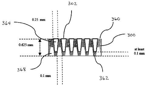
[0086] Figure 4 is a cross-sectional side view of second layer of an exemplary
chip 300 as shown in Figure 3.
Figure 4 shows a non-limiting example of a chip 300 with a thickness of 0.625
mm. Figure 4 also shows the
individual well 302 dimensions as being 0.25 mm (250 gm) in length and width.
As illustrated, the nanowell depth
can be 0.525 mm (525 m), leaving 0.1 mm of the chip beneath a given well. It
is envisioned that nanowell
openings can include a shape such as round, square, rectangle or any other
desired geometric shape. By way of
example, a nanowell can include a diameter or width of between about 100 gm
and about 1 mm, a pitch or length of
between about 150 gm and about 1 mm and a depth of between about 10 gm to
about 1 mm. The cavity of each
nanowell make take a variety of configurations. For instance, the cavity
within a nanowell may be divided by linear
or curved walls to form separate but adjacent compartments.
[0087] The nanowells of the chip may be formed using commonly known
photolithography techniques. The
nanowells may be formed using a wet KOH etching technique or an anisotropic
dry etching technique.
[0088] A nanowell of high inner surface to volume ration may be coated with
materials to reduce the possibility
that the reactants contained therein may interact with the inner surfaces of
the nanowells. A chip can also be made
of resistive heating material. Non-limiting examples of materials include
metal plates such as aluminum and
stainless steel substrates such as SS-316. Where the substrate used is a
metal, it is usually preferable to coat the
surface with an insulating layer to prevent corrosion and/or electrophoresis
of the sample components during
operation with fluid samples. Coating is usually not necessary in the case or
non-metal heating material. A variety
-10-
CA 02677833 2009-08-10
WO 2008/091626
PCT/US2008/000860
of protective coatings are available, including those made of, for example,
Si02, Si3N4, and Teflon. Figure 4 shows
a chip 300 in which the individual wells 302 are etched with KOH and layered
with Si02.
100891 Figure 4 also shows an illustrative chip comprising at least two
opposing arrays of nanowells. In this
figure, the chip 300 has an upper 360 and a bottom 362 surface. One of the
arrays is arranged along the upper
surface 364 and the other is arranged in an opposite array along the bottom
surface 368. The nanowells of the
bottom array are positioned in an inverted manner so that the open surface of
each unit points away from that of the
opposing unit in the chip. The two opposing arrays may be arranged such that
the base of each nanowell is directly
opposite to that of the opposing array.
100901 Though not specifically depicted in Figure 4, any nanowells in the
upper 364 and/or bottom 368 arrays may
be sealed or unsealed. In addition any nanowell in the upper array may be
filled or unfilled, with or without the
reaction sample. The subject chip is then placed in thermal contact with a
heating element by placing the chip in
contact with an external heating element.
100911 The surface of a nanowell of a chip of the invention can further be
altered to create adsorption sites for
reaction reagents. These sites may comprise linker moieties for attachment of
biological or chemical compound
such as a simple or complex organic or inorganic molecule, a peptide, a
protein (for example antibody) or a
polynucleotide. One skilled in the art will appreciate that there are many
ways of creating adsorption sites to
immobilize chemical or biological reactants. For instance, a wealth of
techniques are available for directly
immobilizing nucleic acids and amino acids on a chip, anchoring them to a
linker moiety, or tethering them to an
immobilized moiety, via either covalent or non-covalent bonds (see, for
example, Methods Mol. Biol. Vol. 20
(1993), Beier et al., Nucleic Acids Res. 27:1970-1-977 (1999), Joos et al.,
Anal. Chem. 247:96-101 (1997), Guschin
et al., Anal. Biochem. 250:203-211(1997)). The surface of the nanowell can be
plasma etched to allow for
immobilization of a probe or primer.
100921 As used herein, the term "chemical reaction" refers to any process
involving a change in chemical
properties of a substance. Such process includes a vast diversity of reactions
involving biological molecules such as
proteins, glycoproteins, nucleic acids, lipids, and inorganic chemicals, or
any combinations thereof. The subject
chips have a wide variety of uses in chemical and biological applications
where different temperatures are desired.
The chemical reaction may also involve interactions between nucleic acid
molecules, between proteins, between
nucleic acid and protein, between protein and small molecules. Where the
process is catalyzed by an enzyme, it is
also referred to as "enzymatic reaction."
100931 The subject chips and other apparatus are particularly useful in
conducting enzymatic reactions because
most enzymes function under only certain temperatures. Representative
enzymatic reactions that are particularly
temperature dependent include but are not limited to nucleic acid
amplification, such as quantitative polymerase
chain reaction (qPCR), nucleic acid sequencing, reverse transcription, and
nucleic acid ligation. In an embodiment,
a nucleic acid amplification reaction run on a chip of the invention is a real-
time polymerase chain reaction. In
another embodiment, the nucleic acid amplification reaction is a reverse-
transcription coupled polymerase chain
reaction.
100941 The chips of the present invention provide a cost-effective means for
amplifying nucleic acids. Unlike with
conventional microtiter plates and thermal cyclers, the subject chips are
highly miniaturized, capable of performing
rapid amplification of a vast number of target nucleic acids in small volume,
and under independent thermal
protocols.
100951 As used herein, "nucleic acid amplification" refers to an enzymatic
reaction in which the target nucleic acid
is increased in copy number. Such increase may occur in a linear or in an
exponential manner. Amplification may
-11-
CA 02677833 2009-08-10
WO 2008/091626
PCT/US2008/000860
be carried out by natural or recombinant DNA polymerases such as Taq
polymerase, Pfu polymerase, T7 DNA
polymerase, Klenow fragment of E. coli DNA polymerase, and/or RNA polymerases
such as reverse transcriptase.
[0096] In general, the purpose of a polymerase chain reaction (PCR) is to
manufacture a large volume of DNA
which is identical to an initially supplied small volume of target or seed
DNA. The reaction involves copying the
strands of the DNA and then using the copies to generate other copies in
subsequent cycles. Each cycle will double
the amount of DNA present thereby resulting in a geometric progression in the
volume of copies of the target DNA
strands present in the reaction mixture.
[00971 General procedures for PCR are taught in U.S. Patent Nos. 4,683195
(Mullis) and 4,683,202 (Mullis et al.).
Briefly, amplification of nucleic acids by PCR involves repeated cycles of
heat-denaturing the DNA, annealing two
primers to sequences that flank the target nucleic acid segment to be
amplified, and extending the annealed primers
with a polymerase. The primers hybridize to opposite strands of the target
nucleic acid and are oriented so that the
synthesis by the polymerase proceeds across the segment between the primers,
effectively doubling the amount of
the target segment. Moreover, because the extension products are also
complementary to and capable of binding
primers, each successive cycle essentially doubles the amount of target
nucleic acids synthesized in the previous
cycle. This results in exponential accumulation of the specific target nucleic
acids at approximately a rate of 2n,
where n is the number of cycles.
[0098] A typical conventional PCR thermal cycling protocol comprises 30 cycles
of (a) denaturation at a range of
90 C to 95 C, (b) annealing at a temperature ranging from 50 C to 68 C, and
(c) extension at 68 C to 75 C. With
the subject chips, the thermal cycling time can be drastically reduced because
of, partly, the small reaction volume,
the small heating mass, and the design of effective heat dissipation features.
[0099] The subject chips can be employed in reverse transcription PCR reaction
(RT-PCR). RT-PCR is another
variation of the conventional PCR, in which a reverse transcriptase first
coverts RNA molecules to double stranded
cDNA molecules, which are then employed as the template for subsequent
amplification in the polymerase chain
reaction. In carrying out RT-PCR, the reverse transcriptase is generally added
to the reaction sample after the target
nucleic acids are heat denatured. The reaction is then maintained at a
suitable temperature (for example, 30-45 C)
for a sufficient amount of time (for example, 5-60 minutes) to generate the
cDNA template before the scheduled
cycles of amplification take place. Such reaction is particularly useful for
detecting the biological entity whose
genetic information is stored in RNA molecules. Non-limiting examples of this
category of biological entities
include RNA viruses such as HIV and hepatitis-causing viruses. Another
important application of RT-PCR
embodied by the present invention is the simultaneous quantification of
biological entities based on the mRNA level
detected in the test sample. One of skill in the art will appreciate that if a
quantitative result is desired, caution must
be taken to use a method that maintains or controls for the relative copies of
the amplified nucleic acids.
[00100] Methods of "quantitative" amplification of nucleic acids are well
known to those of skill in the art. For
example, quantitative PCR (qPCR) can involve simultaneously co-amplifying a
known quantity of a control
sequence using the same primers. This provides an internal standard that may
be used to calibrate the PCR reaction.
Other ways of performing qPCR are available in the art.
[00101] Nucleic acid amplification is generally performed with the use of
amplification reagents. Amplification
reagents typically include enzymes, aqueous buffers, salts, primers, target
nucleic acid, and nucleoside
triphosphates. Depending upon the context, amplification reagents can be
either a complete or incomplete
amplification reaction mixture.
[00102] Reagents contained within a chip of the invention depend on the
reaction that is to be run. In an
embodiment, at least one of the units of the array of addressable units
contains a reagent for conducting the nucleic
-12-
CA 02677833 2009-08-10
WO 2008/091626
PCT/US2008/000860
acid amplification reaction. Reagents can be reagents for immunoassays,
nucleic acid detection assays including but
not limited to nucleic acid amplification. Reagents can be in a dry state or a
liquid state in a unit of the chip.
[00103] In an embodiment, at least one of the units of the array of
addressable units of a chip capable of carrying
out a nucleic acid amplification reaction contains at least one of the
following: a probe, a polymerase, and a dNTP.
In another embodiment, the nanowells of a chip contain a solution comprising a
probe, a primer and a polymerase.
In various embodiments, each chamber comprises (1) a primer for a
polynucleotide target within said standard
genome, and (2) a probe associated with said primer which emits a
concentration dependent signal if the primer
binds with said target.
[00104] In various embodiments, each unit comprises a primer for a
polynucleotide target within a genome, and a
probe associated with the primer which emits a concentration dependent signal
if the primer binds with the target.
[00105] In another embodiment, at least one unit of the chip contains a
solution that comprises a forward PCR
primer, a reverse PCR primer, and at least one FAM labeled MGB quenched PCR
probe.
[00106] In an embodiment, primer pairs are dispensed into a unit and then
dried, such as by freezing. The user can
then selectively dispense, such as nano-dispense, the sample, probe and/or
polymerase.
[00107] In other embodiments of the invention, the nanowells may contain any
of the above solutions in a dried
form. In this embodiment, this dried form may be coated to the wells or be
directed to the bottom of the well. The
user can add a mixture of water and the sample to each of the wells before
analysis.
[00108] In this embodiment, the chip comprising the dried down reaction
mixture may be sealed with a liner, stored
or shipped to another location. The liner is releasable in one piece without
damaging the adhesive uniformity. The
liner is visibly different than the cover to aid in identification and for
ease of handling. The material of the liner is
chosen to minimize static charge generation upon release from the adhesive.
When the user is ready to use the chip,
the seal is broken and the liner is removed and the sample is added to the
units of the chip. The chip can then sealed
and placed into contact with a heating element.
[00109] In many applications, sealing the units (for example, nanowells) is
desirable to prevent evaporation of
liquids and thus maintains the preferred reaction concentrations throughout
the thermal cycling.
[00110] The chip may be used for genotyping, gene expression, or other DNA
assays preformed by PCR. Assays
performed in the plate are not limited to DNA assays such as Taqman, Invader,
Taqman Gold, SYBR gold, and
SYBR green but also include other assays such as receptor binding, enzyme, and
other high throughput screening
assays. In some embodiments, a ROX labeled probe is used as an internal
standard.
[00111] The invention also provides a method for performing a PCR analysis
using a chip comprising a plurality of
preloaded nanowells, the method comprising: placing a sample into the
nanowells to create a reaction mixture;
sealing the nanowells of the chip with mineral oil or another sealing
mechanism; placing the chip into a thermal
cycling system; cycling the system; and analyzing results.
1001121 In accordance with the present invention, the units of the chip
comprise a solution operable to perform
multiplex PCR. In a preferable embodiment, the units are capable of having
multiple PCR reactions in each
individual unit based on the chemistry and the probes that are included in the
solution. "Multiplex PCR" is the use of
more than one primer pair in the same unit. This method can be used for
relative quantitation where one primer pair
amplifies the target and another primer pair amplifies the endogenous
reference. A multiplex reaction can be
performed using a variety of methods including the Standard Curve Method or
the Comparative Ct Method.
1001131 Various probes can be used, such as FAM which is a carboxy-fluorescein
which has an excitation
wavelength from about 485 nm and an emission wavelength from about 510- 520
nm; SYBR Green 1 which is
normally used for RT-PCR and has an excitation wavelength of about 488
nanometers and an emission wavelength
-13-
CA 02677833 2009-08-10
WO 2008/091626
PCT/US2008/000860
of about 510 nanometers; TET which has an emission wavelength from about 517
nanometers to about 538
nanometers; the probes from the group of HEX, JOE and VIC, which have emission
wavelengths from 525-535 nm
to about 546-556 nm; TAMRA which is a carboxy-tetra methylrhodamine, and has
an emission wavelength from
about 556 nanometers to about 580 nanometers; ROX which is a carboxy-x-
rhodamine, which has an emission
wavelength from about 575-585 nm to about 605-610 nm; ALEXA, which has an
emission range from about 350
nanometers to about 440 nanometers; TEXAS RED, which has an emission
wavelength from about 580-585 nm to
about 600-610 nm; Cy3, which has an emission wavelength of about 545
nanometers to about 568 nanometers; Cy5,
which has an emission wavelength of about 635- 655 urn to about 665-675 nm;
Cy7, which has an emission
wavelength of about 715 nanometers to about 787 nanometers. Optimized
interference filters precisely match the
excitation and emission wavelengths for each fluorophore to block out unwanted
cross-talk from spectrally adjacent
fluorophores.
1001141 The choice of primers for use in nucleic acid amplification will
depend on the target nucleic acid sequence.
Primers used in the present invention are generally oligonucleotides, usually
deoxyribonucleotides several
nucleotides in length, that can be extended in a template-specific manner by
the polymerase chain reaction. The
design of suitable primers for amplifying a target nucleic acid can be
determined by one skilled in the art.
[00115] For a convenient detection of the amplified nucleic acids resulting
from PCR or any other nucleic acid
amplification reactions described above or known in the art, primers may be
conjugated to a detectable label.
Detectable labels suitable for use in the present invention include any
composition detectable by spectroscopic,
photochemical, biochemical, immunochemical, electrical, optical or chemical
means. A wide variety of appropriate
detectable labels are known in the art, which include luminescent labels,
enzymatic or other ligands. In preferred
embodiments, one will likely desire to employ a fluorescent label or an enzyme
tag, such as digoxigenin, 13-
galactosidase, urease, alkaline phosphatase or peroxidase, avidin/biotin
complex.
1001161 The labels may be incorporated by any of a number of means well known
to those of skill in the art. In one
aspect, the label is simultaneously incorporated during the amplification
step. Thus, for example, PCR with labeled
primers or labeled nucleotides can provide a labeled amplification product. In
a separate aspect, transcription
reaction in which RNA is converted into DNA, using a labeled nucleotide (for
example fluorescein-labeled UTP
and/or CTP) or a labeled primer, incorporates a detectable label into the
transcribed nucleic acids.
[001171 The invention also provides reagents and kits suitable for carrying
out polynucleotide amplification
methods of this invention. Such reagents and kits may be modeled after
reagents and kits suitable for carrying out
conventional PCR, RT-PCR, and other amplification reactions. Such kits
comprise a chip of the invention and a
reagent selected from the group consisting of an amplification reagent, a
detection reagent and combinations thereof.
The kits may comprise reagents packaged for downstream or subsequent analysis
of the multiplex amplification
product. The primers included in the individual units can, independently of
one another, be the same or a different
set of primers comprising the plurality of multiplex amplification primers.
100118] In another embodiment, the oligonucleotide probes are suitable for
detecting single nucleotide
polymorphisms, as is well-known in the art. A specific example of such probes
includes a set of four oligonucleotide
probes which are identical in sequence save for one nucleotide position.
[001191 Each of the four probes includes a different nucleotide (A, G, C and
T/U) at this position. The probes may
be labeled with labels capable of producing different detectable signals that
are distinguishable from one another,
such as different fluorophores capable of emitting light at different,
spectrally- resolvable wavelengths (for example
, 4 differently colored fluorophores).
-14-
CA 02677833 2009-08-10
WO 2008/091626
PCT/US2008/000860
1001201 The primer pairs used in this invention can be obtained by chemical
synthesis, recombinant cloning, or a
combination thereof. Methods of chemical polynucleotide synthesis are well
known in the art and need not be
described in detail herein. One of skill in the art can use the target
sequence to obtain a.desired primer pairs by
employing a DNA synthesizer or ordering from a commercial service.
1001211 Nucleic acid amplification requires a target nucleic acid in a buffer
compatible with the enzymes used to
amplify the target. The target nucleic acid used for this invention
encompasses any reaction samples suspected to
contain the target sequence. It is not intended to be limited as regards to
the source of the reaction sample or the
manner in which it is made. Generally, the test sample can be biological
and/or environmental samples. Biological
samples may be derived from human, other animals, or plants, body fluid, solid
tissue samples, tissue cultures or
cells derived therefrom and the progeny thereof, sections or smears prepared
from any of these sources, or any other
samples suspected to contain the target nucleic acids. Preferred biological
samples are body fluids including but not
limited to blood, urine, spinal fluid, cerebrospinal fluid, sinovial fluid,
ammoniac fluid, semen, and saliva. Other
types of biological sample may include food products and ingredients such as
vegetables, dairy items, meat, meat
by-products, and waste. Environmental samples are derived from environmental
material including but not limited
to soil, water, sewage, cosmetic, agricultural and industrial samples.
1001221 Preparation of nucleic acids contained in the test sample can be
carried out according to standard methods
in the art or procedures described. Briefly, DNA and RNA can be isolated using
various lytic enzymes or chemical
solutions according to the procedures set forth in Sambrook et al. ("Molecular
Cloning: A Laboratory Manual"), or
extracted by nucleic acid binding resins following the accompanying
instructions provided by manufacturers'
instructions.
1001231 The nucleic acid in the reaction sample can be cDNA, genomic DNA or
viral DNA. However, the present
invention can also be practiced with other nucleic acids, such as mRNA,
ribosomal RNA, viral RNA. These nucleic
acids may exist in a variety of topologies. For example, the nucleic acids may
be single stranded, double-stranded,
circular, linear or in form of concatamers. Those of skill in the art will
recognize that whatever the nature of the
nucleic acid, it can be amplified merely by making appropriate and well
recognized modifications to the method
being used.
1001241 In an aspect of the invention, a chip for running a reaction comprises
an array of addressable units each
being configured to run a chemical reaction. The addressable units of the chip
are arranged according to a
predetermined set of temperatures for running the chemical reactions of the
units. At least one of the units is
addressed to indicate the predetermined temperature for running the chemical
reactions within the unit.
1001251 In an embodiment, a plurality of the units are addressed to indicate
the predetermined temperature for
running the chemical reactions. In another embodiment, each of the units is
individually addressed to indicate the
predetermined temperature for running the chemical reaction within said unit.
1001261 The predetermined temperature of a unit of a chip of the invention can
be configured to yield at least 90%
of homogeneous product from the chemical reaction. If the annealing
temperatures are optimized, the configuration
of an addressable chip based upon predetermined reaction temperatures can
significantly improve the yield and
quality of a reaction product. This can be important when a user is interested
in analyzing a large number of nucleic
acids, such as the whole genome of an organism, with a chip and the
apparatuses of the present invention. In an
embodiment, the improved reaction yield plays an important role in the use of
a chip, apparatus, or system of the
invention when used as a medical diagnostic instrument.
1001271 Figure 5 illustrates an example chip 500 of the invention comprising a
set of smaller chips 510. The set of
smaller chips 510, also referred to as a plate 500, are placed in contact with
a thermally insulative frame 530. Each
-15-
CA 02677833 2009-08-10
WO 2008/091626
PCT/US2008/000860
smaller chip 510 represents a different temperature zone, as labeled in Figure
5, in this example, zones 1, 2, 3, 4, 5,
and 6. In an embodiment, the temperature zones correspond to a predetermined
set of annealing temperatures for
conducting polymerase chain reaction within the nanowells 520 of the chip 500.
By separating the overall chip 500
into different temperature zones, a user can increase the specificity of the
reaction within the nanowells 520. For
example, when analyzing an entire genome of a species, a plurality of
temperature zones can allow for more
accurate determination of the genome.
1001281 The subject chips can contain one or more grooves etched in at the
bottom side of the chip. In general, the
grooves are under-trenches, open channels or paths to allow air passage. The
grooves reduce the thermal mass of
the chip, increase the surface area, and thus enhance the thermal performance
of the chips. The grooves can be
fabricated in any shapes, including but not limited to circular, elliptical,
oval, conical, rectangular, triangular, and
polyhedral. The grooves may be further divided by linear or curved walls to
form separate but adjacent channels, or
by circular walls to form inner and outer annular channels. The dimensions of
the grooves will depend on the
overall sizes and depths of the chips. The depths of the grooves may range
from about one tenth to about nine tenths
of the chip depths. The other dimensions, namely widths and lengths, may be
shorter, longer or comparable to the
corresponding dimensions of the chips. In particular, the L-shaped grooves
surround the base of a unit. As the air
flows through the passageways formed by any of the grooves, it removes heat
from the surfaces of unit by passive
heat dissipation, thus increasing the speed of thermal cycling.
1001291 Several factors apply to the selection of a suitable chip substrate.
The substrate is often a good thermal
conductor. A good thermal conductor generally has a thermal conductivity value
higher than 1 Wirrillc I, preferably
higher than 100 W/m-IK-1, more preferably higher than 140 W/m-1K-1. Whereas
the material's thermal conductivity
may be 250 WrnilK-1 or higher, it usually does not exceed 500 W/ni 1K-1.
Second, the substrate must be relatively
inert and chemically stable. Such substrate generally exhibits a low level of
propensity .to react with the reaction
samples employed in the intended application. Moreover, the materials should
also be selected based upon the
ability or feasibility to integrate the thermal control elements onto or
adjacent to them. A variety of materials meet
these criteria. Exemplary materials include but are not limited to metalloids
or semiconductors, such as silicon,
silicates, silicon nitride, silicon dioxide, gallium phosphide, gallium
arsenide, or any combinations thereof. Other
possible materials are glass, ceramics (including crystalline and non-
crystalline silicate, and non-silicate-based
ceramics), metals or alloys, composite polymers that contain dopants (for
example, aluminum oxide to increase
thermal conductivity), or any of a range of plastics and organic polymeric
materials available in the art. In one
embodiment, the nanowells are fabricated in such substrates including Al or SS-
316 as well as similar others.
[00130] In an embodiment, the chips are fabricated using a thermally
conductive polymer. For example, the chips
can be fabricated using polycarbonate, polypropylene, or any other conductive
polymer known to those with skill in
the art.
[00131] The chips can be fabricated by any method as would be obvious to one
skilled in the art. Examples of
method of making a chip of the invention include, but are not limited to,
micro drilling, electric discharge method,
hot embossing, and hot embossing with a tool made from which uses water as
light guide.
[00132] Alternatively, chips of the present invention can be fabricated using
techniques well established in the
Integrated Circuit (IC) and Micro-Electro-Mechanical System (MEMS) industries.
The fabrication process typically
proceeds with selecting a chip substrate, followed by using appropriate IC
processing methods and/or MEMS
micromachining techniques to construct and integrate various components.
[00133] Fabrication of the subject chips can be performed according to
standard techniques of IC-processing and/or
MEMS micromachining. The subject chips can be fabricated as multi-layer
structures. The process generally
-16-
CA 02677833 2009-08-10
WO 2008/091626
PCT/US2008/000860
proceeds with constructing the bottom layer. Then a combination of techniques
including but not limited to
photolithography, chemical vapor or physical vapor deposition, dry or wet
etching are employed to build structures
located above or embedded therein. Vapor deposition, for example, enables
fabrication of an extremely thin and
uniform coating onto other materials, whereas etching allows for mass
production of larger chip structures. Other
useful techniques such as ion implantation, plasma ashing, bonding, and
electroplating can also be employed to
improve the surface properties of the chips or to integrate various components
of the chips. The following details
the fabrication process with reference to the exemplary chip designs depicted
in the figures. The same general
process and the apparent variations thereof are applicable to fabricate any of
the subject chips described herein.
[001341 Figure 4 is a cross-section view of a portion of an exemplary chip
design. In this embodiment, the
nanowell is embedded within a body which is made up of first and second (or
bottom and top) layers of substrates
respectively. The process begins with providing a first layer of substrate
which is generally a heat resistant material
such as glass, Pyrex wafer, or any other suitable materials described herein
or known in the art. The next step is to
create the nanowell that forms the basis of the unit. The nanowell is
generally disposed within the second layer that
is typically a silicon wafer (see, for example, Figure 4). The silicon wafer
may go through several processing steps
prior to being attached to the first layer. For example, the silicon wafer may
be attached to a layer of photoresist to
render the surface more susceptible to chemical etching after exposure to UV
light during the process of
photolithography. The layer of photoresist defines, by precise alignment of
the photo-mask, the size and location of
the nanowell that is to be formed by a subsequent etching step. The silicon
wafer is then etched by a variety of
means known in the art to form the well cavity. A commonly practiced etching
technique involves the use of
chemicals, for example, potassium hydroxide (KOH), which removes the silicon
wafer to form the desired shape.
[00135] Once the nanowells of the subject chips are fabricated, their surface
properties can be improved to suit the
particular application. Where large surface area is desired, the wall of the
nanowell may be further etched by, for
example, a plasma etcher to obtain very fine dendrites of silicon, commonly
referred to as "black silicon". The
presence of black silicon can dramatically increase the effective heating
surface area. The black silicon fabricated at
the base of the nanowell may also serve as an anchor for photon-sensing
devices, temperature sensors and other
control elements.
1001361 As discussed herein, a nanowell of high inner surface to volume ratio
may be coated with materials to
reduce the possibility that the reactants contained therein may interact with
the inner surfaces of the well. The
choice of methods for applying the coating materials will depend on the type
of coating materials that is used. In
general, coating is carried out by directly applying the materials to the
nanowell followed by washing the excessive
unbound coating material. Certain coating materials can be cross-linked to the
surface via extensive heating,
radiation, and by chemical reactions. Those skilled in the art will know of
other suitable means for coating a
nanowell fabricated on chip, or will be able to ascertain such, without undue
experimentation.
1001371 Sample preparation then includes combining the PCR reaction sample
mixture, the labeled primers, and the
sample with a drop of oil which can be individually nano dispensed to prevent
evaporation. The sample is then
dispensed into the individual nanowells using a piezo dispenser and a dew
point dispensing technique.
1001381 To prevent evaporation of aqueous reaction samples, the samples can be
applied to the nanowell at or
around dew point. As used herein, "dew point" refers to a temperature range
where the droplet size does not change
significantly. At dew point, an equilibrium is reached between the rate of
evaporation of water from the sample
droplet and the rate of condensation of water onto the droplet from the moist
air overlying the chip. When this
equilibrium is realized, the air is said to be saturated with respect to the
planar surface of the chip. At one
atmospheric pressure, the dew point is about 14 C. Accordingly, dispensing
aqueous reaction samples is preferably
-17-
CA 02677833 2009-08-10
WO 2008/091626
PCT/US2008/000860
carried out at a temperature no more than about 1 C to about 5 C degrees above
dew point. As is apparent to one
skilled in the art, dew point temperature increases as the external pressure
increases. Therefore, where desired, one
may dispense the reaction samples in a pressured environment to prevent
evaporation.
1001391 Amplified nucleic acids present in the subject chips may be detected
by a range of methods including but
not limited to (a) forming a detectable complex by, for example, binding the
amplified product with a detectable
label; and (b) electrophoretically resolving the amplified product from
reactants and other components of the
amplification reaction.
[00140] In certain embodiments, the amplified products are directly visualized
with detectable label such as a
fluorescent DNA-binding dye. Because the amount of the dye intercalated into
the double-stranded DNA molecules
is typically proportional to the amount of the amplified DNA products, one can
conveniently determine the amount
of the amplified products by quantifying the fluorescence of the intercalated
dye using the optical systems of the
present invention or other suitable instrument in the art. DNA-binding dye
suitable for this application include
SYBR green, SYBR blue, DAPI, propidium iodine, Hoeste, SYBR gold, ethidium
bromide, acridines, proflavine,
acridine orange, acriflavine, fluorcoumanin, ellipticine, daunomycin,
chloroquine, distamycin D, chromomycin,
homidium, mithramycin, ruthenium polypyridyls, anthramycin, and the like.
1001411 In addition to various kinds of fluorescent DNA-binding dye, other
luminescent labels such as sequence
specific probes can be employed in the amplification reaction to facilitate
the detection and quantification of the
amplified product. Probe based quantitative amplification relies on the
sequence-specific detection of a desired
amplified product. Unlike the dye-based quantitative methods, it utilizes a
luminescent, target-specific probe (for
example, TaqMane probes) resulting in increased specificity and sensitivity.
Methods for performing probe-based
quantitative amplification are well established in the art and are taught in
U.S. Patent No. 5,210,015.
[00142] In various embodiments, the chip additionally comprises alignment
features, operable to align or attach a
cover to the chip or to align or attach the chip to a heating element. In
various embodiments, such features comprise
concave or convex features. Such features include pins, ridges, snaps, screws,
and combinations thereof.
1001431 In various embodiments, the chip assembly comprises a temperature
control element, which facilitates the
monitoring or control of the temperature of reaction chambers. Such
temperature control elements include but are
not limited to channels or other structures that facilitate the flow of a
heating or cooling gas through the assembly.
1001441 In another aspect of the invention, a method of conducting a reaction
that involves a plurality of reaction
samples and requires cycling at least two temperature levels is disclosed and
comprises: providing a chip comprising
an array of addressable units each being configured to run a chemical
reaction, wherein the units are arranged
according to a predetermined set of temperatures for running the chemical
reactions of the units, such that at least
one of the units is addressed to indicate the predetermined temperature for
running the chemical reactions within
said unit; placing the plurality of reaction samples into the units of the
chip according to the set of predetermined
temperatures; and controlling a heating element to effect cycling at least two
temperature levels. In one aspect a
method of conducting a chemical reaction can include providing a chip as
described herein where the chip is
configured to receive a reaction sample. A heating element can be provided
that is positionable in relation to the
chip to provide thermal contact between at least one heating element and the
chip. A chemical reaction can be
conducted in the reaction sample by varying the temperature of the chip.
Varying the temperature in the chip can be
effected, for example, by moving at least one heating element in relation to
the chip such that the heating element is
in thermal contact with the chip.
[00145] The method uses a chip of the invention and a thermal cycling
apparatus or the invention. Typically, in the
analysis of an entire genome of an organism, amplification of different genes
or nucleic acid sequences are
-18-
CA 02677833 2009-08-10
WO 2008/091626
PCT/US2008/000860
optimized at different annealing temperatures. These different annealing
temperatures could be grouped into general
zones to improve the sensitivity and specificity of an assay. A chip of the
invention can therefore be addressed
according to one of the annealing temperature zones.
1001461 The selection of the annealing temperature can be a critical component
for optimizing the specificity of a
PCR reaction. The annealing temperatures of different sequences for nucleic
acid amplification can be determined in
a variety of ways. One method is to determine the melting temperature (Tm) of
a nucleic acid sequence. The melting
temperature is the temperature at which one half of the DNA duplex will
dissociate and become single stranded.
When designing a nucleic acid amplification, primer length and sequence are
important in designing the parameters
of a successful amplification. For example, the melting temperature of a DNA
increases both with its length, and
with increasing guanine and cytosine content which can be approximated using a
simple formula.
1001471 The annealing temperature chosen for a PCR reaction depends directly
on length and composition of the
primer(s). The annealing temperature (Ta) can be chosen to be about 5 C below
the lowest Tõ, of the pair of primers
to be used (Innis and Gelfand, 1990). Another example method of calculating
the annealing temperatures is:
Ta Opt = 0.3 x(Tm of primer) + 0.7 x(Tm of product) - 25
where Tm of primer is the melting temperature of the less stable primer-
template pair and Tm of product is the
melting temperature of the PCR product (Rychlik, et al., 1990).
1001481 If the annealing temperature of a PCR reaction is too low, a primer
can anneal to sequences other than the
true target, and can lead to non-specific amplification and consequent
reduction in yield of the desired product. A
consequence of too high an annealing temperature is that too little product
will be made, as the likelihood of primer
annealing is reduced. Another consideration is that a pair of primers with
very different annealing temperatures may
never give appreciable yields of a unique product, and may also result in
inadvertent asymmetric or single-strand
amplification of the most efficiently primed product strand.
1001491 In PCR thermal cycling, the optimum Ta and the maximum Ta range for
each different primer pair and can
vary from gene to gene in a continuous fashion. Typically, the anneal
temperature to produce high quality anneal
for a given primer pair is in a range of 1 to 3 C. If the anneal temperature
is higher, the PCR anneal step can slow
down; if it is lower, the primers might bind to the DNA at sites other than
the desired ones or to other species.
1001501 One method is to "bin" the gene assays; the temperature of a given
assay is assigned to the addressable
portion of the chip with the temperature closest to that of Ta of that given
gene assay. For example, if the apparatus
or chip has 3 temperature zones of 60, 62.5 and 65 C, an assay that has an
optimum behavior Ta = 64 C is assigned
to the 65 C zone.
1001511 The annealing step of a PCR reaction typically occurs in 40 sec or
less, depending partially on the length of
the sequence to be amplified.
[001521 While the PCR is normally started at 5 C below the calculated
temperature of the primer melting point
(Tm), the optimum temperature often can be much higher than the calculated
temperature. In some embodiments, the
annealing temperature must be empirically tested. For example, multiple PCR
reactions with gradually increasing
temperatures can be carried out until the optimal annealing temperature is
determined.
1001531 Many of the genetic sequences in a genome can be grouped into
temperature zones. In an embodiment, the
units of a chip of the invention represent different annealing temperature
zones, for example, the zones are 2 C
increments over the range of 54 to 68 C. The units are then addressed
according to predetermined temperature at
which the annealing step of the PCR reaction will occur.
1001541 After a unit is addressed according to a predetermined temperature,
sample can then be dispersed into the
chip. The sample can be added to the chip by a variety of methods as disclosed
herein.
-19-
CA 02677833 2014-06-20
WO 2008/091626 PCT/US2008/000860
1001551 In various embodiments, a system or chip can additionally comprise a
filling device, which is operable to
facilitate filling of amplification reagents or samples into the addressable
units of the chip. Filling devices among
those useful herein include physical and chemical modalities that direct,
channel, route or otherwise effect filling
reagents or samples into the addressable units.
1001561 In various embodiments, the chip may comprise raised or depressed
regions, for example, features such as
barriers and trenches to aid in the distribution and flow of liquids on the
surface of the chip. In an embodiment, the
filling system comprises capillary channels. The dimensions of these features
are flexible, depending on factors,
such as avoidance of air bubbles upon assembly and mechanical convenience and
feasibility.
1001571 The filling system comprises any apparatus which facilitates the
placement of amplification reagents or
sample on the surface of the chip, preferably effecting placement of such
reagents or sample in addressable units.
Such apparatus among those useful herein include devices for pouring of
reagents or samples onto the surface so as
to substantially cover the entire surface. In an embodiment the filling system
comprises a device for pipetting,
spotting or spraying of reactants to specific reaction chambers (for example,
by use piezoelectric pumps). The filling
system can be a nano-dispenser. In another embodiment, the filling apparatus
comprises a vacuum pump operable to
fill the reaction chambers of the chip. Filling systems may also include
devices for applying centrifugal force to the
chip. In one embodiment, the filling system is in close proximity to or in
fluid communication with a filling device
in the chip. The filling system can operate automatically or according a
protocol from a computer.
APPARATUS
1001581 One aspect of the present invention is the design of an apparatus
configured to receive a miniaturized chip
designed for the multiplexed analyses of individual molecules, and/or
simultaneous performance of a vast number of
chemical reactions. In one embodiment, the present invention provides a highly
automated, miniaturized, analytical
instrument that allows manipulations with precise control of temperature,
evaporation, small-volume reagent
delivery, and/or product detection in a multiplexed fashion.
1001591 The apparatus of one aspect of the invention includes at least one
heating element useful for heating or
cooling a chip. It is to be understood that where the heating element is
configured to reduce the temperature of a
chip, the component functions essentially as a cooling element
1001601 In one embodiment the apparatus includes a base with at least one
heating element positioned on the base.
The heating element can provide a range of useful temperatures. For example,
the heating element can be
configured to provide a temperature in the range between about -20 C to about
120 C as desired.
1001611 The heating element can be configured to receive a chip. In various
embodiments the heating element can
be positioned either below the chip or above the chip. In a particular
embodiment where only one heating element is
= present, the heating element can move relative to the chip. Where
desired, the chip can be stationary.
1001621 Figure 6 is a non-limiting example of a schematic diagram of the one
embodiment of the apparatus.
Figure 6 depicts a base 600 with at least one heating element 602 positioned
on the base 600. The heating element
602 is adapted to receiving a chip 650, such chip is capable of containing and
confining a reaction sample in one of
the nanowells 652 on the chip 650. The heating element 602 of the apparatus
can be moved in two positions relative
to the chip 650.
1001631 The heating element 602 as seen in Figure 6 can be divided into
different temperature zones as seen in
Figure 7. Figure 7 is an illustrative drawing of a hearing element 700
positioned below the chip used to control
and/or vary the temperature of a chip. In one embodiment the temperature
ranges for a heating element can be in the
range of 90 C to 95 C for the denaturation temperature, 52 C to 65 C for the
primer annealing stage, and 68 C to
-20-
CA 02677833 2009-08-10
WO 2008/091626
PCT/US2008/000860
75 C for the primer-dependent extension stage. A non-limiting example of a
heating element 700 is shown in
Figure 7. The heating element 700 in this example is one with temperature
zones of 95 C (702), 52 C (704), and
72 C (706) for the denaturation, primer annealing stage and primer-dependent
extension stage of PCR, respectively.
The dimensions of each temperature zone of the heating element 700 can vary in
size. In one embodiment depicted
in Figure 7, the heating element positioned below an example of the chip is
about 9 inches in length by 9 inches in
width.
[00164] A chip adapted to containing and confining a reaction sample is then
placed on the heating element 700 of
the apparatus adapted to receiving the chip. Using the heating element
positioned below 700 the chip of Figure 7,
the heating elements then physically moved so that the chip comes in contact
with the 95 C-block, followed by the
52 C-block, and then the 72 C-block. The movement of the heating element
respective to the chip allows the
critical ramp down rates to be a lot faster due to the larger surface area on
the heating element. The larger surface
area also allows for cooling from the backside of the chip due to transfer of
the chip from temperature to
temperature. This technique also allows the chip to be heated and cooled at a
much faster rate than the traditional
way of simply cooling the chip between cycles.
[00165] Another method for controlling and/or varying the temperature of the
chip 800 is depicted in Figure 8.
Figure 8 is a non-limiting example of the heating element 850 positioned above
the chip 800. As shown in Figure 8,
the heating element can be a series of on/off arc halogen lamps 852 positioned
above the chip 800. Heat reflectors
854 are positioned around each halogen lamp 852 to ensure a uniform heat
source from the heat lamps 852. The
high output power of the arc lamp 852 and the spectral match of the output to
silicon provides a very fast "ramp up"
rate of the arc lamps 852. The fact that the lamp is an arc lamp means that
switch off of the arc lamp 852 is virtually
instantaneous. Figure 8 also shows that the chip 800 can also be sealed with a
radiation curable adhesive 802 to help
prevent evaporation of the reaction sample. Following a reaction cycle, in one
non-limiting example the chip is then
scanned with a scanner 860, for example, a hyper spectral or CCD Scanner. In
certain aspects, such an optically
coupled system transmits excitation beams into the wells containing the
reaction samples at a plurality of times
during the amplification, and monitors the optical signals coming from the
nanowells at each of the plurality of
times between cycles.
[00166] Figure 9 graphically shows the change in temperature in Celsius (y-
axis) versus time in seconds (x-axis) of
the on/off arc lamps. As seen in Figure 9, the halogen lamps ramp up rate of
the arc lamp is 20 C to 100 C/ sec for
a temperature of 95+/-0.5 C in less than about 2 seconds and has a 20 C to 100
C ramp down rate to 65+/-0.5 C,
also in less than about 2 seconds. The temperature of the arc lamp shifts from
approximately 65 C to approximately
95 C during the PCR reaction process.
[00167] Where desired, the subject devices are designed to minimize the
movement of pulsed heat into the
nanowells fabricated out of Aluminum/Silicon in an alternative chip. One way
to minimize the amount of pulsed
heat is to reduce the time that the Al/Si spends at the highest temperatures
and thereby reducing "thermal budget".
Speeding the "ramp-up" and "cool-down" rates and providing the fastest
possible transition from heating to cooling,
or "turn around" is therefore important. This method of heating and cooling
the chip also ensures uniformity in the
heating of the chip. Such uniformity prevents stresses due to temperature
differences of a few degrees that can lead
to variations in the performance of the nanowells.
[00168] As seen in Figure 10, there are several temperature output profiles
that the arc lamps are capable of
delivering. The graphs along row (a) show the change in temperature (y-axis)
versus the change in time (x-axis).
Correspondingly, the graphs along row (b) depict the chip response to the
rapid thermal processing (RTP) profiles
depicted in row (a). In response to a slower change in temperature over time,
such as in a spike or impulse optical
-21-
CA 02677833 2009-08-10
WO 2008/091626
PCT/US2008/000860
heater profile, the chip temperature remains constant over the entire depth of
the chip. in response to a more rapid
change in temperature over time, such as in a laser or flash assist heater
profile, the temperature of the chip varies
depending on the depth of the chip relative to the heating source.
[00169] Without being limited to a particular theory, Figure 10 illustrates a
number of temperature output profiles
corresponding to the invention. The spike heater profile, as seen in Figure
10(a)(1), which is characterized by a
rounded thermal profile, generates a chip response temperature similar to the
heating source temperature, as seen in
Figure 10(b)(1). In the impulse heater profile (Figure 10(a)(2)),
characterized by a peaked thermal profile, the
temperature of the heat source is faster than the temperature of the chip in
response to the heat source, but the
temperature of the chip is still kept relatively uniform over the entire depth
of the chip relative to the distance from
the heat source (Figure 10(b)(2)). For a laser heater profile as seen in
Figure 10(a)(3), characterized by a sharply
peaked profile, the heat source acts much faster than the chip. Therefore,
only the surface layer of the chip is heated
(Figure 10(b)(3)). The deeper the depth of the chip, the cooler the
temperature profile. Finally, for the flash assist
profile (Figure 10(a)(4)), characterized by initial bulk heating followed by a
flash for surface annealing, the chip
response is similar to the chip response to the laser profile (Figure
10(b)(4)).
[00170] In another aspect of the invention, an apparatus is described for
conducting a chemical reaction requiring
cycling at least two temperature levels, that comprises: a chip for running a
reaction comprising an array of
addressable units each being configured to run a chemical reaction, wherein
the units are arranged according to a
predetermined set of temperatures for running the chemical reactions of the
units, such that at least one of the units
is addressed to indicate the predetermined temperature for running the
chemical reactions within said unit; and a
heating element in thermal contact with the chip.
[00171] In a preferable embodiment, the addressable units of the chip are
configured to run a nucleic acid
amplification reaction, including but not limited to real-time PCR. The units
can be nanowells that comprise a
reagent, a probe, a primer, a dNTP, or a combination thereof. The
predetermined temperatures can be different
annealing temperatures for carrying out a PCR reaction.
[00172] The heating element can be a simple heater, such as a plate comprising
a resistive heater or a thermoelectric
heater, or an elaborate thermal cycling apparatus. In some examples, the
heating element is thermal contact with a
heat sink to allow for rapid temperature changes of the chip when the chip is
in thermal contact with the heating
element. A fan could also be coupled to the heating element to provide more
control over rapid thermal cycling.
Other examples of heating elements include thin film heaters that can be
heated rapidly by conduction or have
electromagnetic heaters incorporated into the film. A material particularly
suitable for fabricating the thin film
heaters is indium tin oxide (ITO). ITO is a transparent ceramic material with
a very high electrical conductivity.
Because ITO can be prepared in bulk or in form of thin layer, it is
particularly useful as seither an integral or an
external heating element.
[00173] In another embodiment, heating elements are compatible to the chips in
terms of size and configuration. In
an embodiment, the apparatus further comprises a plurality of heating
elements. The heating element can be placed
as a detachable unit adjacent to, at the base and/or on top of the chip. In a
preferable embodiment, the heating
element area is significantly larger than the chip area, in order to minimize
edge effects at the edges of a heating
element.
[00174] Some examples of heating element construction and setup are
illustrated in Figures lla-c. In these
examples, the heating elements 1100 are coupled to a heat sink 1110 and a fan
1120 to improve control over
temperature changing and ramp up times for thermal cycling. A metal thermal
block 1130 can be used between the
heating element 1100 and the sample (or chip) 1140 that is in intimate thermal
contact with the element 1100 and
-22-
CA 02677833 2009-08-10
WO 2008/091626
PCT/US2008/000860
the chip 1140. The block 1130 can have a high thermal conductivity even if the
chip 1140 might not have a high
thermal conductivity, to produce a reproducible temperature change. If
multiple heating elements are used to define
a temperature zone or multiple temperature zones, any small disturbance of the
heating (for example, an air breeze)
can produce a significant change in temperature. If the resistance is made low
using a thermal block, the transfer of
heat from zone to zone can be smoothed. In addition, the metal thermal block
can hold temperature sensors on the
top surface. The temperature sensor can correspond to each zone, or can be
part of the chip itself. The thermal block
can also provide vacuum channels to allow vacuum to hold the chip in intimate
thermal contact with the block
and/or heating elements. As demonstrated in Figures lla-c, the heating element
1100 can comprise one or a
plurality of thermoelectric 1150 or resistive 1160 heating elements, or a
combination of both.
[00175] The heating element can provide a temperature gradient. The
temperature gradient herein can be a
temperature that is higher in a portion than another portion across a single
heating element. For example, a resistive
or thermoelectric heater can be configured to create a thermal gradient across
the heating element. The thermal
gradient can also be defined as a temperature that is higher in one portion
than another portion of the chip. For
example, if a plurality of heating elements are used, one heating element
could deliver a higher temperature to one
side or end of the chip and a second heating element could deliver a different
temperature to one side or end of the
chip, thereby creating a thermal gradient.
[00176] The apparatus can further comprise an optical system operatively
coupled to the chip, wherein the optical
system detects an optical signal coming from a unit. In one exemplary
embodiment, the chip, heating element, and
optical system make up a system of the invention.
[00177] In an aspect, the invention disclosure includes an apparatus for
conducting a chemical reaction involving
cycling at least two temperature levels comprising: a body configured to
receive a sample holder for containing the
chemical reaction; a first heater comprising a plurality of temperature zones;
and a second heater providing a
uniform temperature, wherein the first heater and the second heater are
configured to be movable between a first and
a second orientation, and wherein the first orientation places the heater in
thermal contact with the sample holder
and the second orientation does not place the heater in thermal contact with
the sample holder.
[00178] The sample holder can be a chip for running a reaction comprising an
array of addressable units each being
configured to run a chemical reaction, wherein the units are arranged
according to a predetermined set of
temperatures for running the chemical reactions of the units, such that at
least one of the units is addressed to
indicate the predetermined temperature for running the chemical reactions
within said unit. In an embodiment, the
plurality of temperature zones correspond to the predetermined set of
temperatures according to which the units are
arranged.
[00179] In an embodiment where the apparatus and sample holder are configured
to conduct a PCR reaction, the
predetermined temperature zones correspond to different annealing temperatures
at which multiple PCR reactions
can be run. In a further embodiment, the apparatus and sample holder are
capable of conducting a series of PCR
reactions in order to amplify most, if not all, of a genome. In this example,
an entire genome requires a range of
annealing temperatures to achieve the desired specificity of a reaction. For
example, these temperatures can be
grouped into 2 C temperature zones according to the annealing temperatures of
different nucleotide sequences. The
units of a sample holder can be addressed according to the temperature zone at
which the reaction within the unit is
to be run. In an embodiment, the apparatus receives a sample holder that
comprises a chip with units addressed
according to six different annealing temperature zones corresponding to six
different temperature zones on the first
heater of the apparatus.
-23-
CA 02677833 2009-08-10
WO 2008/091626
PCT/US2008/000860
[00180] In a preferable embodiment, the first and second heaters move between
the first and second orientations
according to a protocol. The apparatus can further comprise a motor for moving
the first and second heaters between
the first and second orientations. The heaters can be moved by any method as
would be obvious to those skilled in
the art.
[00181] The first orientation puts a heater in thermal contact with the sample
holder. In an embodiment, the sample
holder is used to conduct a PCR reaction. The first heater has a plurality
temperature zones, and can be used to
provide the temperatures necessary for the annealing steps of a PCR reaction
when the first heater is brought into
thermal contact with the sample holder. In an embodiment, the second heater
provides a temperature necessary for
elongation or denaturation of a nucleic acid during a PCR reaction when the
second heater is in the first orientation
and thermal contact with a sample holder.
[00182] In an example of the apparatus and method of the invention, the second
heater is moved into the first
orientation in thermal contact with the sample holder for a PCR reaction. The
second heater delivers a temperature
of around 95 C, in order to denature a nucleic acid in a sample contained
within the sample holder. After the
denaturation step, the second heater is moved into the second orientation and
the first heater is moved into the first
orientation in thermal contact with the sample holder. The first heater
provides temperatures to the sample holder
for the annealing of a primer to a nucleic acid sequence of the sample. The
process of conducting a denaturation
step followed by an annealing step can be repeated or cycled until the desired
amplification product is achieved.
[001831 Figure 12 demonstrates an example embodiment of a thermal cycling
apparatus 1200 of the invention. In
this example, the apparatus 1200 comprises a first heater 1210 with 6
different temperature zones corresponding to 6
different addressable predetermined temperatures of a chip 1250. The first
heater 1210 can be moved in and out of
thermal contact with the chip 1250 as shown in the top view in Figure 12. The
second heater 1220 provides a
uniform temperature across the entire heater in order to heat each of the 6
different addressable predetermined
temperature areas of the chip 1250 to the same temperature. For example, the
second heater 1220 can provide
uniform temperatures for the denaturation and elongation steps of conducting
PCR with a chip of the invention,
while the first heater 1210 can provide a range of annealing temperatures to
increase the specificity of conducting a
large number of reactions. An imaging source 1260 for analyzing the many
reactions can be positioned on the
opposite side of the chip from the first orientation of the heaters.
[00184] Figure 13 demonstrates a side view of the first heater 1210 from the
example in Figure 12 when the heater
1210 is in the first orientation in thermal contact with a chip with
addressable units 1250. For example, each
temperature zone 1212, 1214 of the heater can be provided by a different
thermoelectric heating element 1216, 1218
and some example specifications are shown in Figure 13.
[00185] In an embodiment, the first heater can provide a temperature gradient.
Examples of types of heaters for the
first and second heaters include, but are not limited to, a resistive heater
and a thermoelectric heater.
[00186] In a further embodiment, the apparatus comprises a heat sink in
thermal contact with the first heater, the
second heater, or both.
[00187] In order to monitor temperature, the apparatus can also comprise a
plurality of temperature sensors. In an
embodiment, the plurality of temperature sensors have at least one temperature
sensor assigned to measure the
temperature of each temperature zone of the apparatus. The temperature sensor
can be a thermocouple or any other
sensor that are available in the art.
[00188] The heating element can be connected via electric leads to a power
source that provides voltage across the
element and effects subsequent heating of the units. The heating element may
also be coupled to a temperature
sensor that monitors and regulates the temperature of the unit. The
temperature sensor may control the temperature
-24-
CA 02677833 2009-08-10
WO 2008/091626
PCT/US2008/000860
and hence the thermal profile of an array of units. Dividing the chip and/or
first heater into various temperature
zones provides additional flexibility for parallel performance of chemical
reactions that require different thermal
cycling profiles. Alternatively, the temperature sensor can be coupled to
individual unit or zone so that the
temperature of each unit or zone can be independently controlled. The
temperature sensor may be included as a
detachable unit located adjacent to or at the base of the unit. It can also be
integrated into the interior or the exterior
surface of the unit. Furthermore, the temperature sensor can be fabricated as
an integral part of the heating element.
[001891 A temperature profile provided by a thermal cycling apparatus of the
invention is demonstrated in Figure
14. In this example, the 6 different temperature zones of the first heater are
represented by separate lower
temperatures than the 95 C uniform temperature provided by the second heater.
For example, when amplifying an
entire human genome with the chips, systems, and apparatuses of the invention,
40 cycles can be performed in less
than about 15 minutes, 10 minutes or even 5 minutes in order to amplify every
gene (about 30,000) of the genome.
[00190] The body of the apparatus for providing cycling at least two
temperature levels is configured to receive a
sample holder. The sample holder can be held in place within the body by a
variety of means, including vacuum
force. In an embodiment, the body comprises a vacuum chuck for holding the
sample holder firmly in place
allowing for a heater to be placed into thermal contact with the sample
holder. Clamps, pins, adhesives, slots, or any
other method of securing can be incorporated into the body as configured to
receive the sample holder as would be
obvious to those skilled in the art.
1001911 The apparatus can also further comprise sensors to determine the
position of the first and second
orientations of a heating element in respect to the sample holder.
1001921 In another aspect of the invention, an apparatus for conducting a
chemical reaction involving cycling at
least two temperature levels comprises: a body configured to receive a chip
comprising a plurality of nanowells for
containing the chemical reaction; and a first heater providing a first
temperature and a second heater providing a
second temperature, wherein the first heater and the second heater are
configured to be movable between a first and
a second orientation, and wherein the first orientation places the heater in
thermal contact with the sample holder
and the second orientation does not place the heater in thermal contact with
the sample holder.
[00193j In an embodiment, the plurality of nanowells are addressable, wherein
the nanowells are arranged
according to a predetermined set of temperatures, such that at least one of
the nanowells is addressed to indicate the
predetermined temperature for running the chemical reaction within said
nanowell.
[00194] In another embodiment, the first heater comprises a plurality of
temperature zones. The plurality of
temperature zones can correspond to the predetermined set of temperatures
according to which the units are arrayed.
[00195] The first and second heaters can move between the first and second
orientations according to a protocol. In
an embodiment, the apparatus can further comprise a motor for moving the first
and second heaters between the first
and second orientations.
[00196] In an embodiment, the first heater can provide a temperature gradient.
Examples of types of heaters for the
first and second heaters include, but are not limited to, a resistive heater
and a thermoelectric heater.
[00197] In a further embodiment, the apparatus comprises a heat sink in
thermal contact with the first heater, the
second heater, or both.
1001981 In order to monitor temperature, the apparatus can also comprise a
plurality of temperature sensors. In an
embodiment, the plurality of temperature sensors have at least one temperature
sensor assigned to measure the
temperature of each temperature zone of the apparatus.
[00199] An exemplary apparatus and system 1500 of the invention is illustrated
in Figure 15. A chip 1510 can be
loaded into an apparatus for conducting a chemical reaction involving cycling
at least two temperature levels. The
-25-
CA 02677833 2009-08-10
WO 2008/091626
PCT/US2008/000860
chip 1510 can be set in place by any method capable of holding them in place,
such as a vacuum or a clip. The chip
can also be placed within the apparatus by sliding the chip into place against
a stop or a wall, which aligns the chip
in a proper position. The chip can be placed on a sample holder 1520 that is
capable of moving up and down. The
sample holder can be configured to couple to a heater 1530 of the apparatus
1500.
1002001 In an embodiment, the chip 1510 and/or wells of the chip are sealed by
a thin plastic cover 1512, e.g., a
standard PCR tape for covering a chip or a nanowell plate. The PCR tape can be
made of a transparent material,
such as polyethylene, and can be removable and sometimes can be replaceable.
Transparent oil can also be used to
cover the wells and/or surface of the chip 1510. In an embodiment, the chip
1510 and/or wells are covered by oil
and a cover.
1002011 In an embodiment, the cover 1512 covering the chip 1510 is not removed
before placing the chip into a
thermal cycling apparatus of the invention. After the chip is in place within
the apparatus, the heater 1530 can
provide a force to the chip 1510 that brings the chip 1510 into optical or
thermal contact with a top cover slide 1540.
The top cover slide 1540 can be made of a transparent material or any material
that allows optics to view a reaction
of the chip. Materials that can be used as the top cover slide include, but
are not limited to, glass, silica, silicon, and
polymers or plastics as would be obvious to those skilled in the art.
1002021 The top cover slide 1540 may also comprise a heater 1542, such as an
indium tin oxide (ITO) heater, that
can heat the top of the chip 1510 or the cover of the chip 1512 and/or wells.
A heater 1542 of the top cover slide can
be used to balance the temperature at the surface of the chip such that
condensation does not occur at the surface or
opening of a unit on the chip. For example, when a PCR reaction is run, the
liquid components of the reagents
and/or sample may heat to a point where they condense on the surface or cover
of the reaction unit, or reaction well.
Condensation can interfere with an optical system used to monitor the reaction
within the unit. In an embodiment of
the invention, as demonstrated in Figure 15, the heater 1530 of the apparatus
can provide a force that brings the chip
1510 into thermal contact with a top cover slide 1540 comprising a heater
1542, which can balance the temperature
at the surface of the chip 1510 to prevent condensation. Also shown in Figure
15, the top cover slide 1540 may be
connected to a bridge 1550 of the apparatus by a pair of springs or
compressive devices 1552. The springs or other
devices 1552 can relieve some of the pressure on the top cover slide 1540 from
the force of the heater 1530 against
the chip 1510, making the apparatus and system more robust. Any method of or
device for pressure damping may be
used to couple the top cover slide to a bridge of the apparatus.
1002031 In the exemplary system and apparatus in Figure 15, a chip 1510 can be
unloaded or loaded through the
side of the thermal cycling apparatus 1500. A heater 1530 of the apparatus can
then be moved into an orientation in
thermal contact with the chip 1510 and also provide a force that brings the
chip into thermal contact with a top cover
slide 1540. In Figure 15, the chip has a plastic cover 1512 covering the
wells. Also in Figure 15, the top cover slide
1540 comprises fused SiO2/Quartz material and also comprises an ITO heater
1542. The ITO heater 1542 is
operated by electric leads 1544 connected to the ITO heater as shown in Figure
15. The top cover slide 1540 is then
connected to a bridge 1550 of the apparatus by a compressive spring 1552 that
provides stress relief within the
system. The spring 1552 can also serve to improve the thermal contact of the
chip 1510 to both a heater 1530 of the
apparatus and a heater of the top cover slide 1540.
1002041 In practice, controlling a heating element and hence the temperature
of the reaction sample, can be effected
by processing a predetermined algorithm stored on a computer readable medium
operatively linked to the heating
element. The movement of a heating element can also be controlled by a
protocol or algorithm, which can be
provided by a computer or stored on a computer readable medium. In other
aspects, the controlling step may involve
processing temperature or movement sensor signals retrieved from a temperature
sensor element that is operatively
-26-
CA 02677833 2009-08-10
WO 2008/091626
PCT/US2008/000860
linked to a unit of a sample holder or chip based on protocols stored on a
computer readable medium. This can be
achieved by employing conventional electronics components for temperature
control that may process either analog
or digital signals. Preferably, the electronics components are run on a
feedback control circuitry. They can control
the temperature of one unit, but more often the temperature of multiple units
that collectively form one temperature
zone or the temperature of the zone itself. In certain embodiments, the
temperatures of the different zones are
separately controlled. The thermal cycling profile and duration will depend on
the particular application in which
the subject chip is to be employed.
SYSTEMS
1002051 The subject chips can be provided with an optical system capable of
detecting and/or monitoring the results
or the progress of chemical reactions taking place in the chips. Such optical
system achieves these functions by first
optically exciting the reactants, followed by collecting and analyzing the
optical signals from the reactants of the
chip. The optical system applicable for the present invention comprises three
elements, namely the optical
excitation element, the optical transmission element, and the photon-sensing
element. The optical system may also
comprise, optionally, an optical selection element.
1002061 Figure 16 is a representative block diagram showing a representative
example of the instrumentation in an
experimental setup. Figure 16 shows a computer system (or digital device) 1600
connected to a laser 1610 as a
representative example of an optical excitation element. The optical
excitation element acts as the source of
excitation beams used to optically excite the reactants contained in the
nanowells. This element encompasses a wide
range of optical sources that generate light beams of different wavelengths,
intensities and/or coherent properties.
Representative examples of such optical excitation sources include, but are
not limited to, lasers, light-emitting
diodes (LED), ultra-violet light bulbs, and/or white light sources.
1002071 The optical transmission element used in the present invention serves
two functions. First, it collects
and/or directs the optical excitation sources to the reactants inside the
nanowells of the chips. Second, it transmits
and/or directs the optical signals emitted from the reactants inside the
nanowells of the chips to the photon-sensing
element. The optical transmission element suitable for use in the present
invention encompasses a variety of optical
devices that channel light from one location point to another. Non-limiting
examples of such optical transmission
devices include optical fibers, optical multiplexers (MUX) and de-multiplexers
(DE-MUX), diffraction gratings,
arrayed waveguide gratings (AWG), optical switches, mirrors, lenses,
collimators, and any other devices that guide
the transmission of light through proper refractive indices and geometries.
1002081 The photon-sensing element analyzes the spectra of the optical signals
coming from the reactants inside the
nanowells. Suitable photon-sensing element can detect the intensity of an
optical signal at a given wavelength, and
preferably can simultaneously measure the intensities of optical signals
across a range of wavelengths. Preferably
the element may also provide spectrum data analyses to show the spectrum peak
wavelength, spectrum peak width,
and background spectrum noise measurements. Representative examples of
suitable photon-sensing element for the
present invention are avalanche photo diodes (APD), charge-coupled devices
(CCD), electron-multiplying charge-
coupled device (EMCCD), photo-multiplier tubes (PMT), photo-multiplier arrays,
gate sensitive FET's, nano-tube
FET's, and P-I-N diode. As used herein, CCD includes conventional CCD,
electron-multiplying charge-coupled
device (EMCCD) and other forms of intensified CCD.
1002091 While the subject optical systems can be assembled using many
combinations of the various elements, a
useful assembly for analyzing the spectra of the excited reactants comprises
an optical transmission element and a
photon-sensing element. Such assembly is also referred to herein as "spectrum
analyzer".
-27-
CA 02677833 2014-06-20
WO 2008/091626 PCT/US2008/000860
1002101 Where desired, the optical system of the present invention can include
an optical selection element. This
element selects and/or refines the optical properties of the excitation beams
before they reach the reactants contained
in the nanowells. The optical selection element can also be employed to select
and/or refine the optical signals
coming from the reactants in the nanowells before the signals reach the photon-
sensing element. Suitable optical
selection element can select and modify a wide range of optical properties,
including but not limited to, polarization,
optical intensities, wavelengths, phase differences among multiple optical
beams, time delay among multiple optical
beams. Representative examples of such optical selection elements are
polarization filters, optical attenuators,
wavelength filters (low-pass, band-pass or high-pass), wave-plates and delay
lines.
1002111 The aforementioned optical elements can adopt a variety of
configurations. They can form integral parts of
the subject chips or remain as separate units. All of these elements are
commercially available. Accordingly, in one
embodiment, the present invention provides a chip in which the optical
transmission and photon-sensing elements
are fabricated into the chip substrate. In one aspect, the photon-sensing
element is integrated into each nanowell on
the chip that is to be monitored. In another aspect, more than one type of
photon-sensing element is integrated into
the nanowell to enhance the detection capability or efficiency. In another
aspect, the photon-sensing element can be
fabricated along the side or at the base of the nanowell, or as part of the
cover of the nanowell. Photon-sensing
elements suitable for such configuration include but are not limited to
avalanche photo diode, charge coupled
devices (including conventional CCD, electron-multiplying charge-coupled
device (EMCCD) and other forms of
intensified CCD), gate sensitive FET's, nano-tube FET's, P-I-N diode.
Avalanche photo diode is particularly
preferred because it permits detections of a single photon by amplifying the
signal through an avalanche process of
electron transfer. These elements together with the supporting circuitry can
be fabricated as part of the subject chips
using standard IC processing techniques described herein or known in the art.
1002121 In another embodiment, the present invention provides an apparatus in
which the chip and the optical
systems remain as separate units. One aspect of this embodiment encompasses an
apparatus for conducting a
chemical or biological reaction requiring cycling at least two temperature
levels over a multiple-cycle period. The
apparatus comprises a chip of the present invention, and an optical system
that is operatively coupled to the chip and
that detects an optical signal coming from the nanowell. Preferably, the
optical signals detected are related to the
amount of product of the chemical reaction taking place in the nanowell.
1002131 Figure 16 illustrates an exemplary optical system of this aspect In an
exemplary embodiment, this system
includes an optical transmission element, such as a tunable laser 1610, or
Xenon lamp, controlled by the computer
or other digital setup 1600. The laser is then focused further to provide
uniform distribution across all the nanowells
using a Powell lens 1620, a telescope 1630, and/or a line focused laser 1640.
The optical signals coming from the
nanowells on the chip are collimated by a lens 1690, such as a tube lens, and
are passed through a tunable filter
1680, either a low-pass, high-pass, or notch-filter, to a charge-coupled
device (CCD) 1615 for spectrum analysis.
This particular embodiment offers a low cost solution for monitoring the
progress and/or results of chemical
reactions taking place in nanowells fabricated on a chip.
1002141 In a further embodiment the optical transmission element is moveable
being placed on a X-Y stage, as seen
in Option 1 of Figure 16. In an alternative embodiment, the chip is placed on
an X-Y stage as seen in Option 2 of
Figure 16.
1002151 In a further embodiment feedback control or self learning is provided
to achieve optimized chemical
reactions at specific nanowells of the substrate. For example, using a fixed
position substrate including an array of
nanowells in conjunction with a moveable optical transmission element and
photon-sensing element, after heating
(or providing a series of heating and/or cooling steps) with one or more
optical transmission units, the photon-
-28-
CA 02677833 2009-08-10
WO 2008/091626
PCT/US2008/000860
sensing element can detect the outcome of a desired chemical reaction in a
specific nanowell. Upon analysis of each
chemical reaction in a given nanowell based on the detection step, suitable
corrections (for example, raising or
lowering reaction temperatures or durations of reaction cycles) can be
implemented in subsequent cycle rounds of
heating and/or cooling to optimize the chemical reaction as needed. This
process can be repeated using repeated
passes of the transmission element and sensing element over the various
nanowell locations until the desired
outcome of a chemical reaction is detected in each nanowell. In this way a
given nanowell chemical reaction can be
sequentially monitored and manipulated to provide an optimized chemical
reaction for the given nanowell.
Different conditions may be required at different nanowell locations based on
the unique properties of the individual
reactions (for example, where different primers and templates are used in a
PCR reaction). Thus, the apparatus of
the present invention can be used in conjunction with a feed back loop process
directed to each nanowell location, to
optimize the chemical reaction at every location on a substrate.
[00216] In an exemplary embodiment, a Chungara series CCD camera can be used.
The Chungara CCD camera can
be used for the most demanding applications in low noise and long exposure
imaging in areas such as astronomy
and spectroscopy. The Chungara CCD controller is able to read a wide range of
CCDs, because it is based on
modularity and common hardware architecture. For instance, example CCDs that
can be used range from the
1536x1024 Kodak KAF-1602 CCD to the 4096x4096 Kodak KAF-16801 CCD. The camera
can be linked to a host
computer thru an ethernet link or wireless connection allowing a large
distance between the computer and the CCD
camera.
[00217] In another embodiment, the present invention provides a system in
which the chip, apparatus and the
optical systems are separate units. In one embodiment, the apparatus, system,
chip of the present invention, a
thermal cycling apparatus or heating element of the invention, and an optical
system that is operatively coupled to
the chip and that detects an optical signal corning from an addressable unit
of the chip. Preferably, the optical signals
detected are related to the amount of product of the chemical reaction taking
place in the unit.
[00218] In another preferable embodiment, the amplified nucleic acids in the
subject chips are detected by the
subject optical systems operatively coupled to the chips. The optical systems
are capable of transmitting appropriate
excitation beams to the reactants in the amplification reactions, collecting
and analyzing the emitted optical signals
from the reactants. Preferably, the optical signals detected are indicative of
the amount of amplified nucleic acid in
the amplification reaction over a multiple-cycle period. In certain aspects,
the optical system transmits excitation
beams into the wells containing the reaction samples at a plurality of times
during the amplification, and monitors
the optical signals coming from the nanowells at each of the plurality of
times. By analyzing the relative intensities
of the optical signals, preferably over a multiple-cycle period, one can
monitor quantitatively the progression of the
amplification reaction. Typically, the optical signals being monitored are
luminescent signals. Detecting and/or
monitoring the amplification products can be performed without opening the
nanowell once the amplification is
initiated.
1002191 Figure 17 demonstrates an example system 1700 of the invention with a
thermal cycling apparatus 1710
with a first 1712 and second heater 1712 that can be moved between a first and
second orientation, and a chip 1720
with an addressable array of units based on predetermined temperatures. In
this example, the optical system 1730
operatively coupled to the chip 1720 and apparatus 1710 is a Chungara CCD
camera 1732. As shown by the side
view in Figure 17, the heaters 1712, 1714 can move independently and brought
into thermal contact with a chip
1720 of the invention to provide rapid thermal cycling of a large number of
chemical reactions, such as PCR
amplification reaction of an entire genome.
-29-
CA 02677833 2009-08-10
WO 2008/091626
PCT/US2008/000860
[002201 Figure 18 demonstrates an example system 1800 of the invention
comprising an optical system 1810, a
heating apparatus 1820, and a chip 1830 for conducting a chemical reaction.
The heating apparatus 1820 of the
system may be a thermal cycling device for conducting a PCR reaction. As shown
in Figure 18, the heating
apparatus can comprise a denature block 1822 and an anneal block 1824 for
conducting PCR. The heating apparatus
1820 is also movable both horizontally and vertically as indicated by the
arrows in Figure 18. A chip 1830 is
inserted on a sample holder 1840 that can move vertically. The chip 1830
and/or nanowells of the chip may or may
not be covered by a plastic cover 1832. The heater 1820 can force the sample
holder 1840 into thermal contact with
a top cover slide 1850 comprising a thin film ITO heater 1852. The top cover
slide 1850 is connected to the system
1800 by a compressive spring 1854 to permit better thermal contact between the
sample holder 1840 and heaters
1820, 1852 of the system. The system 1800 may also comprise a dead stop 1856
to prevent the top cover slide 1850
from compressing into the optical system 1810.
[00221] In Figure 18, the optical system 1810 comprises a CCD camera 1812, an
excitation light source 1814,
optics 1816, and an optical filter 1818. The system may comprise a plurality
of optical systems. In another
embodiment, the system comprises a plurality of CCD camera, excitation light
sources, optics, or optical filters. The
optical system 1810 can function to receive information from a chemical
reaction that occurs in the chip 1830 when
the chip 1830 is in thermal contact with the heating apparatus 1820.
1002221 Figure 19 is a block diagram showing a representative example logic
device through which reviewing or
analyzing data relating to the present invention can be achieved. Such data
can be in relation to a genotype, a
genetic make up or a disease, disorder or condition in an individual. Figure
19 shows a computer system (or digital
device) 1900 connected to an apparatus 1920 for use with an apparatus 1924 to,
for example, produce a result. The
computer system 1900 may be understood as a logical apparatus that can read
instructions from media 1911 and/or
network port 1905, which can optionally be connected to server 1909 having
fixed media 1912. The system shown
in Figure 19 includes CPU 1901, disk drives 1903, optional input devices such
as keyboard 1915 and/or mouse 1916
and optional monitor 1907. Data communication can be achieved through the
indicated communication medium to
a server 1909 at a local or a remote location. The communication medium can
include any means of transmitting
and/or receiving data. For example, the communication medium can be a network
connection, a wireless connection
or an interne connection. Such a connection provide for communication over the
World Wide Web. It is
envisioned that data relating to the present invention can be transmitted over
such networks or connections for
reception and/or review by a party 1922. The receiving party or user 1922 can
be a patient, a health care provider or
a health care manager. In one embodiment, a computer-readable medium includes
a medium suitable for
transmission of a result of an analysis of a biological sample. The medium can
include a result regarding a
genotype, a genetic make up or a disease condition or state of a subject,
wherein such a result is derived using the
methods described herein.
USES OF THE PRESENT INVENTION
[00223] The subject chips and apparatuses for thermal cycling have a wide
variety of uses in chemical and
biological applications where controllable temperatures are desired. The
methods, chips, and apparatuses of this
invention are preferably performed with equipment which aids in coupling one
or more steps of the process,
including handling of the chips, thermal cycling, and imaging. Accordingly,
the present invention provides systems
for simultaneously determining the genetic expression profile in a biological
sample obtained from an individual
member of a species relative to a standard genome for said species.
-30-
CA 02677833 2009-08-10
WO 2008/091626
PCT/US2008/000860
[00224] In one embodiment, the invention can be used to vary and/or maintain
temperature of a reaction sample.
Varying and/or maintaining temperature of a reaction sample are required in a
wide range of circumstances
including but not limited to discerning protein-protein interaction, examining
DNA or RNA hybridization, and
performing enzymatic reaction. The method involves placing the reaction sample
into a nanowell fabricated in a
chip that is in thermal contact with a heating element, and applying a voltage
to the heating element.
[00225] In another embodiment, the subject chips apparatuses for thermal
cycling are used for conducting a
chemical reaction that involves a plurality of reaction samples and requires
cycling at least two temperature levels.
The process involves (a) providing a chip comprising an array of units as
described herein; (b) placing the plurality
of reaction samples into the units of the chip; and (c) controlling the
heating element to effect cycling at least two
temperature levels.
[00226] Practicing the subject method generally proceeds with placing the
reaction sample into a nanowell of the
subject chip that is in thermal contact with a heating element. Where desired,
the reaction sample can be applied by
a dispensing system operatively coupled to the subject chip. A variety of
dispensing instruments, ranging from
manually operated pipettes to automated robot systems are available in the
art. Preferred dispensing instruments
include a piezo-electric nano-dispenser.
[00227] The subject chips and apparatuses are particularly suited for
conducting quantitative nucleic acid
amplification. Accordingly, the present invention provides a method for
monitoring the formation of a nucleic acid
amplification reaction product, preferably in real time. In certain preferred
embodiments, the amplified nucleic
acids contained are directly monitored by the photon-sensing elements
integrated into the chips. The photon-sensing
element registers the intensities of the optical signals that are reflective
of the amount of the amplified nucleic acids
at any time being examined during the amplification reaction. The optical
signals may be any kind of luminescent
signals emitted upon exciting the labeled reactants with appropriate incident
beams.
[00228] The subject methods of amplifying and detecting a target nucleic acid
have broad spectrum of utility in, for
example drug screening, disease diagnosis, phylogenetic classification,
genotyping individuals, parental and forensic
identification.
[00229] In an embodiment, a system, chip, apparatus, or method of the
invention can be used to discover
therapeutically-relevant biomarkers. For example, the invention could be used
to identify biomarkers for chronic
obstructive pulmonary disease (COPD) and lung cancer.
[00230] At a more fundamental level, amplification and detection of the target
nucleic acids may be used in
identification and quantification of differential gene expression between
diseased and normal tissues, among
different types of tissues and cells, amongst cells at different developmental
stages or at different cell-cycle points,
and amongst cells that are subjected to various environmental stimuli or lead
drugs.
[002311 In various configurations of the present invention, a method is
disclose for supplying to a consumer assays
useful in obtaining structural genomic information, such as the presence or
absence of one or more single nucleotide
polymorphisms (SNPs), and functional genomic information, such as the
expression or amount of expression of one
or more genes. As such, the assays can be configured to detect the presence or
expression of genetic material in a
biological sample. The method includes providing a user interface configured
for receiving orders for stock assays,
providing a user interface configured for receiving requests for design of
custom assays and for ordering said assays,
and delivering to the consumer at least one custom or stock assay in response
to an order for the one custom or stock
assay placed by the consumer. In certain other aspects, the present invention
includes a system, apparatus, chip, and
methods for constructing a system for providing to a consumer assays
configured to detect presence or expression of
genetic material. In an embodiment, the chips can be customized according to a
user's needs.
-31-
CA 02677833 2009-08-10
WO 2008/091626
PCT/US2008/000860
1002321 The present invention provides devices and methods for containing and
handling small quantities of
liquids, including methods and devices for performing amplification reactions
on liquid samples containing
polynucleotides. Embodiments of the present invention include chips for
conducting a chemical reaction, including a
thermocycled amplification reaction of polynucleotide, in a liquid sample.
1002331 The subject chips and other devices find utility in many other
chemical and biological applications where
controllable temperatures are desired. Such applications include a vast
diversity of reactions such as redox
reactions, hydrolysis, phosphorylation, and polymerization. Additional
applications are directed to discerning
interactions involving biological molecules such as proteins, glycoproteins,
nucleic acids, and lipids, as well as
inorganic chemicals, or any combinations thereof. The chemical reaction may
also involve interactions between
nucleic acid molecules, between nucleic acid and protein, between protein and
small molecules The chemical
reaction may take place outside a cell or inside a cell that is introduced
into a nanowell of the subject chip.
1002341 Of particular significance is the application in detecting the
presence of a specific protein-protein
interaction. Such application generally employs a proteinaceous probe and a
target protein placed in a unit in the
subject chip.
1002351 In one aspect of this embodiment, the protein-protein interaction is
between a target protein (for example an
antigen) and an antibody specific for that target. In another aspect, the
protein-protein interaction is between a cell
surface receptor and its corresponding ligand. In yet another aspect, the
protein-protein interaction involves a cell
surface receptor and an immunoliposome or an immunotoxin; in other aspects,
the protein-protein interaction may
involve a cytosolic protein, a nuclear protein, a chaperon protein, or
proteins anchored on other intracellular
membranous structures.
10023611 The terms "membrane", "cytosolic", "nuclear" and "secreted" as
applied to cellular proteins specify the
extracellular and/or subcellular location in which the cellular protein is
mostly, predominantly, or preferentially
localized.
1002371 "Cell surface receptors" represent a subset of membrane proteins,
capable of binding to their respective
ligands. Cell surface receptors are molecules anchored on or inserted into the
cell plasma membrane. They
constitute a large family of proteins, glycoproteins, polysaccharides and
lipids, which serve not only as structural
constituents of the plasma membrane, but also as regulatory elements governing
a variety of biological functions.
[002381 The reaction is typically performed by contacting the proteinaceous
probe with a target protein under
conditions that will allow a complex to form between the probe and the target.
The conditions such as the reaction
temperature, the duration of the reaction, the buffer conditions and etc.,
will depend on the particular interaction that
is being investigated. In general, it is preferable to perform the reactions
under physiologically relevant temperature
and buffer conditions. Physiologically relevant temperatures range from
approximately room temperature to
approximately 37 C. This can be achieved by adjusting the heating element of
the subject chips. Typically, a
physiological buffer contains a physiological concentration of salt and at
adjusted to a neutral pH ranging from
about 6.5 to about 7.8, and preferably from about 7.0 to about 7.5. A variety
of physiological buffers is listed in
Sambrook eta!. (1989) supra and hence is not detailed herein.
[002391 The formation of the complex can be detected directly or indirectly
according standard procedures in the art
or by methods describe herein. In the direct detection method, the probes are
supplied with a detectable label and
when a complex is formed, the probes emitted an optical signal distinct from
that of the unreacted probes. A
desirable label generally does not interfere with target binding or the
stability of the resulting target-probe complex.
As described above, a wide variety of labels suitable for such application are
known in the art, most of which are
-32-
CA 02677833 2014-06-20
WO 2008/091626 PCT/US2008/000860
luminescent probes. The amount of probe-target complexes formed during the
binding reaction can be quantified by
standard quantitative assays, or the quantitative methods using the optical
systems described above.
1002401 The examples and other embodiments described herein are exemplary and
are not intended to be limiting in
describing the full scope of apparatus, systems, compositions, materials, and
methods of this invention.
The scope of the claims should not be limited to these illustrative
embodiments but should
be given the broadest interpretation consistent with the description as a
whole.
-33-