Note: Descriptions are shown in the official language in which they were submitted.
CA 02678682 2009-08-14
WO 2008/103784 PCT/US2008/054512
-1-
APPARATUS, SYSTEM AND METHOD FOR HIGH RESOLUTION IDENTIFICATION
WITH TEMPERATURE DEPENDENT RESISTIVE DEVICE
FIELD OF THE INVENTION
The invention relates in general to temperature dependent resistive devices
and
more specifically to an apparatus, system, and method for high resolution
identification
with temperature dependent resistive devices.
BACKGROUND
Many systems and circuits utilize temperature sensing elements (TSEs) to
determine a temperature of a device. For example, typical temperature
dependent
resistive devices (TDRD) such as thermistors may have resistances that are
inversely
proportional to temperature. By measuring the resistance of the thermistor,
the
temperature of the thermistor can be determined. As a result, temperatures of
components and devices near the thermistor can also be determined or
estimated.
Resistance sensing techniques are sometimes used as identification techniques
to
determine the identity of a device, module, or other peripheral unit that is
connected to a
main device or main assembly. For example, portable communication devices that
accept more than one type of modular battery include a battery identification
technique to
determine the type of battery that is connected to the portable communication
device. In
order to minimize components and contacts, conventional designs often combine
temperature sensing techniques and identification techniques. For example,
some
conventional portable communication devices that accept more than one type of
modular
battery include a temperature sensing mechanism that connects to circuits
within the
battery packs to determine temperature and to identify the battery module.
Each type of
battery module includes thermistor circuits having different characteristics
allowing the
portable communication device to identify the particular battery module that
is connected.
Typically, each thermistor circuit has a resistance to temperature
relationship that is
offset from relationships of other thermistor circuits within other types of
battery modules.
Conventional systems are limited, however, in that the resistance-to-
temperature
relationships of different circuits typically overlap. FIG. 1, for example, is
a graphical
illustration showing two curves 102, 104 representing the resistance vs.
temperature
CA 02678682 2009-08-14
WO 2008/103784 PCT/US2008/054512
-2-
relationship for two conventional battery modules where the curves overlap.
The overlap
region 106 results in ambiguous data since a measurement of a resistance
within the
overlap region is associated with both of the curves 102, 104. The measurement
may
correspond to one type of battery module at a low temperature or another type
of battery
module at a higher temperature. For example, resistance R may correspond to a
temperature of T1 if one battery module is used and a temperature of T2 if
another
battery is connected. This error could lead to catastrophic results. A battery
could
explode where a battery module is inaccurately identified and an incorrect
charging
scheme is applied. Further, the dynamic range and accuracy of the temperature
measuring circuit is reduced as the number of identification devices is
increased as well
as requiring a unique voltage-to-temperature transfer function for each of the
possible
curves. In addition, these problems are exacerbated as the number of IDs is
increased.
Accordingly, there is a need for an apparatus, system and method for high
resolution identification with temperature dependent resistive devices.
SUMMARY
A temperature measuring and identification (TMID) device obtains
identification
information and temperature information of a connected device having a
temperature
sensing circuit (TSC). The TSC includes a temperature sensing element (TSE)
connected in parallel with a voltage clamping network (VCN) that limits the
voltage
across the TSE to an identification voltage within an identification voltage
range when the
voltage is greater than or equal to a lower voltage of the identification
voltage range.
When a voltage below the lower range is applied to the TSC, the VCN appears as
an
open circuit and the resistance of the TSC corresponds to temperature. A
translation
circuit within the TMID shifts TSC voltages within the identification voltage
range to a
normalization voltage range. Accordingly, voltages corresponding to
temperature as well
as voltages corresponding to identification are within the normalization
voltage range. As
a result, the resolution of a voltage sensing device used for measuring the
temperature
and identification voltages is maximized. In addition, the translation circuit
maintains a
minimal current during a rest state. For cost or other concerns, a first TSC
may omit the
CA 02678682 2009-08-14
WO 2008/103784 PCT/US2008/054512
-3-
VCN to provide a maximum identification voltage and other TSCs may include
VCNs with
lower identification voltage ranges.
BRIEF DESCRIPTION OF THE DRAWINGS
FIG. 1 is a graphical illustration of a resistance to temperature relationship
of two
conventional identification and temperature sensing circuits.
FIG. 2A is a block diagram of a temperature sensing circuit (TSC) connected to
a
measuring temperature measuring and identification device (TMID device) in
accordance
with the exemplary embodiment.
FIG. 2B is a block diagram of a translation circuit in accordance with the
exemplary embodiment.
FIG. 3A is a graphical illustration of the voltage (VDp) at the detection port
during
measuring, diagnostic, and identification procedures in accordance with the
exemplary
embodiment.
FIG. 3B is a graphical illustration of the voltage (VDp) and a translated
voltage
range for a system having four identification values in accordance with the
exemplary
embodiment.
FIG. 4 is a schematic representation of an exemplary implementation of the
temperature measuring and identification device (TMID device) where the
translation
circuit includes field effect transistors (FETs).
FIG. 5 is a graphical illustration of a relationship between the currents and
voltages in a translation circuit in accordance with the exemplary embodiment.
FIG. 6 is a block diagram of a plurality of temperature sensing circuits
(TSCs) of
an identification system including four identification values (IDs) in
accordance with the
exemplary embodiment.
DETAILED DESCRIPTION
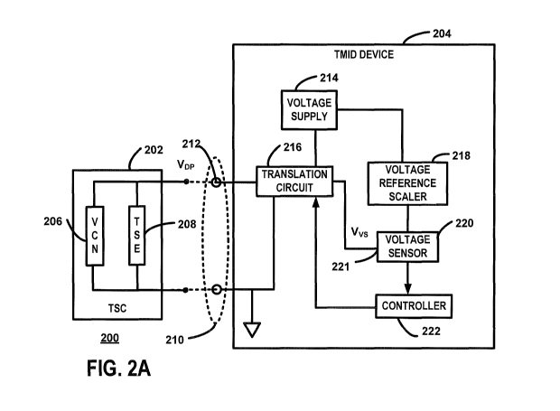
FIG. 2A is a block diagram of a temperature sensing circuit (TSC) 202
connected
to a temperature measuring and identification (TMID) device 204 to form a
temperature
measuring and identification circuit 200. As discussed in further detail
below, the TSC
202 is one TSC of a set of TSCs where the characteristics of the TSCs allow
the TMID
CA 02678682 2009-08-14
WO 2008/103784 PCT/US2008/054512
-4-
device 204 to distinguish between the different sets of TSCs. The TSCs can be
installed
within different devices providing a mechanism for monitoring the temperature
of a
device and for identifying the device. An example of suitable application of
the
temperature measuring and identification circuit 200 includes installing a
different TSC
within each type of battery module accepted by a portable device. The TMID
device 204
can be implemented as part of portable device to identify different types of
battery
modules and to determine the temperature of the battery module.
Each TSC 202 includes at least a temperature sensing element (TSE) 208. At
least one TSCs of a TSC set includes a voltage clamping network (VCN) 206
connected
in parallel to the TSE 208. In the exemplary embodiment, a linearization
resistor (not
shown in FIG. 2) is also connected in parallel to the TSE 208 in all of the
TSCs in order
linearize the temperature to resistance curves of the TSC 202.
The TMID device 204 connects to the TSC 202 through a connection interface
210 that includes at least a detector port 212. The connection interface 210
may include
any of numerous types of connectors, contacts, or electrical connection
mechanisms to
provide an electrical connection between the TMID device 204 and the TSC 202.
The
exemplary connection interface 210 also includes a ground connector.
Additional
contacts may be used for other signals in some circumstances.
As described below, each set of TSCs of the plurality of TSCs includes a
different
VCN where the VCN may include any combination of resistors and/or voltage
clamping
devices, such as diodes. The VCN may be omitted from one set of TSCs to create
an
identification value (ID) that is not voltage clamped. When the TSC is
connected to the
TMID device 204, the voltage at the detection port 212 depends on the
particular VCN
206, the temperature, and the status of voltage source 214 in the TMID device
204. The
VCN limits the detector port voltage to a voltage within an ID voltage range.
The number
of ID voltage ranges depends on the number of TSC sets that can be connected
to the
TMID device 204.
The TMID device 204 includes a voltage supply 214 connected to the detection
port 210 through a translation circuit 216. A voltage reference scaler 218
scales the
supply voltage to a voltage that is less than the supply voltage to provide a
reference
voltage to a voltage sensor 220. A controller 222 is configured to control the
translation
CA 02678682 2009-08-14
WO 2008/103784 PCT/US2008/054512
-5-
circuit 216 and to receive a voltage measurement from the voltage sensor 220.
In
response to a control signal, the translation circuit 216 provides an
identification voltage
bias to the TSC 202 during a device identification state and a temperature
voltage bias
during a temperature measuring state. During the identification state, the
translation
circuit 216 shifts the voltage at the TSC to the normalization voltage range.
Based on the
voltage measurement and the status of the control signal, the controller 222
determines
the temperature of the TSE 208 and an ID of the TSC 200 from a plurality of
IDs. As
discussed below, the voltage sensor 220 and the controller 222 are implemented
within a
processor in the exemplary embodiment.
The TMID device 204 controls the voltage at the detection port (VDP) by
switching
transistors within the translation circuit 216. During the identification
state, a sufficiently
high current is applied to the detection port to invoke the voltage clamping
function of the
VCN 206 while a scaling network scales the clamped voltage to a corresponding
value
within the normalization voltage range. During the temperature measuring
state, the
current into the detection port is sufficiently reduced to prevent the voltage
clamping
function allowing the voltage sensor 218 to measure the resistance of the TSE
which is
used to determine the temperature. In this temperature measuring state, the
voltage
(VpP) measured by the voltage sensor 220 at the detection port 212 is
processed by the
controller 222 to determine the temperature of the TSE 208 or to determine
that an error
condition exists. Where the detected voltage is within a temperature measuring
voltage
range, the voltage (VDp) at the detection port corresponds to the resistance
of the TSE
208 and the controller 222 calculates the temperature based on the detected
voltage. If
the voltage is outside the range, the controller 222 determines that an error
condition
exists.
The voltage sensor 220 is an analog to digital converter (ADC) in the
exemplary
embodiment. The voltage reference scaler 218 provides a reference voltage that
is at or
near the maximum value of the normalization voltage range. Accordingly, the
number of
quantization levels of the ADC used for measuring voltage is increased. The
increased
resolution improves the accuracy of the measurements. For example, if the
supply
voltage is equal to Vdd and the reference voltage to the ADC is Vdd/2, the
normalization
voltage range may be set to 0 to Vdd/2 and all of the quantization levels of
the ADC are
CA 02678682 2009-08-14
WO 2008/103784 PCT/US2008/054512
-6-
distributed between 0 and Vdd/2. As compared to a system that does not shift
the VDP
voltage to a normalization voltage range, the ADC resolution and accuracy will
be almost
double.
FIG. 2B is a block diagram of a translation circuit 216 in accordance with the
exemplary embodiment. Although the functional blocks shown in FIG. 2B may be
implemented using any combination of firmware hardware and/or software, the
translation circuit 216 includes an arrangement of transistors and resistors
as well as
other electrical components in the exemplary embodiment. The translation
circuit 216
comprises an ID bias circuit 224, a temperature measuring bias circuit 226 and
a scaling
network 228. During the identification state, the control signal activates the
ID bias circuit
224 and the temperature measuring bias circuit 226 to provide a sufficiently
high voltage
at the detection port 212 to activate the VCN 206. As explained below in
further detail, a
network of transistors and resistors connected to the supply voltage 214
establish a bias
voltage as the detection port 212. The resulting voltage (VDP) at the
detection port
depends on the particular VCN 206. The scaling network 228 scales the voltage
to a
corresponding value within the normalization voltage range.
In the temperature measuring state, the control signal is changed to a level
that
deactivates the ID bias circuit 224. The temperature measuring bias circuit
226, however,
remains active and provides a voltage that is less than the ID voltage range
of the VCN
206. In the exemplary embodiment, a charge storage element, such as capacitor,
maintains an appropriate control voltage at the temperature measuring bias
circuit 226
for a time sufficiently long to allow a measurement of the detection port
voltage. The
scaling network is at least partially inactivated to maximize the dynamic
range of the
detection port voltage.
FIG. 3A is a graphical illustration of the voltage (VDp) at the detection port
212
during measuring, diagnostic, and identification procedures. FIG. 3B is a
graphical
illustration of the voltage (Vvs) at the input 221 to the voltage sensor 220
and a
relationship 334 between the detection port voltage (VpP) and the voltage
sensor input
voltage (Vvs). The various values and ranges depicted in FIG. 3A and 3B are
not
necessarily to scale and are provided to generally illustrate relationships
between
different voltages and temperatures during different conditions. The graphical
illustrations
CA 02678682 2009-08-14
WO 2008/103784 PCT/US2008/054512
-7-
show an example of the relationship 334 between the detection port voltage and
the
voltage at the input to the voltage sensor 220 where the translation circuit
shifts the VDP
voltages to a normalization voltage range 303. In the interest of brevity and
clarity values
shown in FIG. 3A and 3B may be approximations of actual values observed in
practice
due to characteristics of the components of the TMID. For instance, the
illustrated
example indicates that the translation circuit does not shift the detection
port voltages
during the temperature measuring state and the detection port voltage appears
at the
input of the voltage sensor 220. The actual voltage at the voltage sensor
input 221,
however, may vary from the detection port voltage as result of voltage drops
due to
current flowing into the voltage sensor 220.
During the temperature measuring state, only the temperature measuring bias
circuit is active and the voltage (VDP) indicates a temperature or an error
condition. If the
voltage (VDP) is above an upper temperature measuring voltage (VUTM) 302 of
the
temperature measuring voltage range (VMR) 304, the voltage sensor 220 detects
a
voltage (Vvs) that is at maximum quantization level and the controller 222
determines
that no TSC 202 is connected to the TMID device 204. If the voltage (VDP) is
at or near
the supply voltage (Vdd) of the TMID device 204, for example, the voltage
indicates that
no current is flowing through the detection port 212 and that no circuit is
connected to
TMID device 204. The corresponding voltage (Vvs) at the voltage sensor input
221 is
above the reference voltage (VREF) 336 and the ADC is "railed" high. If the
voltage is
below a lower temperature measuring voltage (VTLM) 308 of the temperature
measuring
voltage range (VMR) 304, the controller 222 determines that something other
than a valid
and properly operating TSC is connected to the TMID device 204. For example, a
voltage near zero can indicate a short circuited detection port 212 that may
be due to a
failed TSC or an invalid TSC device that is not intended to be connected to
the TMID
device 204. If, during the temperature measuring state, the voltage (VDP) is
within the
temperature measuring voltage range (VMR) 304, the voltage (VDp) and the input
voltage
(Vvs) correspond to a temperature of the TSE 202 where the temperature may be
measured between a minimum temperature (TMiN) 310 and a maximum temperature
(TMAx) 312. In the exemplary embodiment, where the TSE is an NTC thermistor, a
maximum voltage (VUTM) corresponds to the minimum temperature (TMiN). The
CA 02678682 2009-08-14
WO 2008/103784 PCT/US2008/054512
-8-
relationship between detector port voltage (VoP) and temperature follows a
temperature
curve 301. The shape of the curve 301 depends on the temperature sensing
element
(TSE) 208 characteristics as well as other components in the circuit. In the
exemplary
embodiment, a linearization resistor is connected in parallel with the TSE 208
in order to
make the curve 301 more linear as compared to a TSC that includes a TSE
without a
linearization resistor.
During the identification state, the detection port voltage (VpP) corresponds
to an
identification value (ID) of the TSC 202. The scaling network 228 shifts the
detection port
voltage (VpP) to within the normalization voltage range 303. The voltage
sensor input
voltage (VvS) corresponding to the detection port voltage indicates the ID of
the TSC 202.
In the exemplary embodiment, the scaling network 228 slightly compresses the
detection
port ID voltage range. As explained in further detail below, the scaling
network includes a
voltage divider in the exemplary embodiment resulting in a non-zero minimum
value of
the shifted voltage sensor input voltage. A detection port voltage above the
upper
temperature measuring voltage (VUTM) 302 is associated with one of at least
two ID
voltages or ID voltage ranges. The number of voltage IDs depends on the number
of
TSCs in the set of TSCs that may be connected to the TMID device 204. When
both bias
circuits 224, 226 are active, the controller 222 determines the ID of the TSC
202 based
on the voltage (Vvs) at the voltage sensor that corresponds to the voltage
(VpP) at the
detection port 212. The bias circuits 224, 226 and voltage supply 214 are
configured to
provide a detection port voltage above the upper temperature measuring voltage
temperature (VUTM) 302 when the voltage source 214 is on. An example of a
suitable
scheme includes having one TSC that does not include a VCN and that results in
a first
ID voltage (VID1) that is near the maximum voltage 306 and that corresponds to
a first
(ID1), a second TSC that includes a VCN that limits the voltage near VuTM 302
to define
a second ID (ID2), and additional TCSs that include VCNs that result in ID
voltage
ranges that are between the ID voltage (VID1) and the second ID voltage
(VID2). The
maximum number of ID voltage ranges depends on the available voltage range
between
the VuTM and the maximum voltage 306 as well as the size of the ID voltage
ranges. The
maximum voltage 306 is the voltage corresponding to the minimum temperature
since
the thermistor has a maximum resistance at the minimum temperature. As
explained
CA 02678682 2009-08-14
WO 2008/103784 PCT/US2008/054512
-9-
below, the various components are selected such that the worst case maximum
voltage
of the thermistor is less than conduction voltage of the VCN that occurs at
the lowest
operating temperature.
FIG. 3A and FIG. 3B illustrate an exemplary system that supports four IDs
although any combination and number of ID voltages may be used to group TSCs
into ID
categories. A first ID voltage 306 results when a first type TSC that does not
include a
VCN is connected to the TMID device 204 and the voltage source 214 is on. A
second ID
voltage results within a voltage range 314 when a second type TSC that
includes a VCN
is connected to the TMID device 204 and the voltage source 214 is on. ID
voltages result
within a third voltage range 316 and a fourth voltage range 318 when a third
type TSC
and a fourth type TSC are connected to the TMID device 204, respectively.
The translation circuit 216 shifts the ID voltage ranges of the detection port
to
normalized ID voltage ranges at the voltage sensor input 221. Therefore, each
upper ID
voltage 322, 326, 330 and each lower ID voltage 320, 324, 328 of each ID
voltage range
314, 316, 318 are shifted to a corresponding lower normalized ID voltage 338,
340, 342
and upper normalized ID voltage 344, 346, 348 of corresponding normalized ID
voltage
range 350, 352, 354, respectively. When the voltage sensor 220 indicates a
voltage (Vvs)
at the input 221 that is within a normalized ID voltage range, the controller
222
determines that the TSC connected to the TMID device has an ID corresponding
to the
normalized ID voltage range. Therefore, the controller 222 determines that the
TSC has
one of four IDs for the scheme illustrated in FIG. 3A and FIG. 3B. As
discussed below,
the IDs associated with an ID voltage range correspond to the TSCs that
include VCNs.
Since the voltage clamping devices within the VCN, such as diodes, have a
forward
voltage threshold that varies between devices and over temperature, the ID
voltage
resulting from a particular TSC may vary from a lower voltage to an upper
voltage of the
corresponding ID voltage range. Accordingly, the second ID voltage range 314
includes a
lower voltage (VIDL2) 320 and an upper voltage (VIDUZ) 322, the third ID
voltage range
316 includes a lower voltage (VIDL3) 324 and an upper voltage (VIDU3) 326, and
the
fourth ID voltage range 318 includes a lower voltage (VIDL4) 328 and an upper
voltage
(VIDU4) 330.
CA 02678682 2009-08-14
WO 2008/103784 PCT/US2008/054512
-10-
FIG. 4 is a schematic representation of an exemplary implementation 400 of the
temperature measuring and identification circuit 100 where the voltage sensor
220, and
the controller 222 are implemented within a processor 402. The various
components and
functions described above with reference to FIG. 1 can be implemented using
other
combinations of hardware, software, and/or firmware. In the exemplary
implementation,
the controller 222 controls a general purpose input/output (GPIO) port 404 of
the
processor 402 to generate the control signal. The processor 402 may be any
type of
general purpose processor, application specific integrated circuit (ASIC), or
other
microprocessor or processor arrangement, that can perform the functions
described
herein. Code running on the processor 402 facilitates the functions of the
controller 222
as well as other functions of the TMID device 204. In the example discussed
with
reference to FIG. 4, the transistors are field effect transistors (FETs).
Other types of
transistors or switching elements may be used in some circumstances to perform
the
described functions.
The controller 222 controls the GPIO port 404 to place the GPIO port 404 in an
output (on) state and an off state. In the output state, the GPIO port 404
provides a
voltage at or near the supply voltage (Vdd). In the off state, the GPIO port
404 presents a
voltage at or near ground (OV). As described below in further detail, the
control signal,
having a voltage (VCONT) 406, activates transistors within the translation
circuit 216 to
place the circuit 216 in a rest state or an identification (ID) state. Circuit
elements within
the translation circuit 216 enable a temperature measuring state during a time
period
when the translation circuit 216 transitions from the ID state to the rest
state. An analog-
to-digital converter (ADC) 408 measures the voltage (VApc) at the output 410
of the
translation circuit 216 by providing the controller 222 with a digital
representation of the
voltage (VADC). The elements of the TSC 202 form circuits with the translation
circuit 216
where the detection port voltage (VpP) corresponds to the ADC-measured voltage
(VADC)
to allow a temperature measurement in the temperature measuring state and an
identification value (ID) when the translation circuit 216 is in the ID state.
Any one of at least two TSCs 202 can be connected to the TMID device 204. FIG.
4 illustrates a TSC 202 that includes a linearization resistor (RLiN) 412, a
TSE 208 and a
VCN 206, where the TSE 208 is a thermistor 208 and the VCN 206 includes an
CA 02678682 2009-08-14
WO 2008/103784 PCT/US2008/054512
-11-
identification resistor (R,p) 414 in series with a voltage clamping device
416. In the
exemplary implementation, the voltage clamping device 416 is a diode
arrangement 416
that includes one or more diodes that have a forward voltage within a forward
voltage
range. The voltage range depends on the number and type of diodes. For
example, a
typical PN junction, silicon diode has a forward voltage of approximately 0.7
volts. Two
silicon diodes in series will have a collective forward voltage of about 1.4
volts. Due to
manufacturing variations and other factors, the forward voltage of a
particular diode may
be greater than or less than the expected voltage drop. Further, the forward
voltage
varies over temperature. Accordingly, a voltage range is defined for the diode
arrangement 416 where any particular diode arrangement will have a forward
voltage
within the range. Examples of other suitable diode arrangements include
arrangements
using single Zener diodes and active Zener diodes. Zener diodes can be used
with
reverse bias to maintain a fixed voltage across their terminals. In addition,
the voltage
clamping variations of Zener diodes are typically less than the forward
voltage variations
of PN junction silicon diodes over temperature, bias current and manufacturing
variations. Active Zener diodes may be preferred in some circumstances since
active
Zener diodes, also known as "shunt regulators" have variations in clamping
voltages
lower than normal Zener diodes.
During the rest state of the TMID 204, the GPIO port 404 is set to a control
voltage (VCONT) 406 at or near the supply voltage (Vdd). In the exemplary
embodiment,
the first field effect transistor (FET1) 418 and the second field effect
transistor (FET2)
420 are P channel FETs. Accordingly, when the GPIO port 404 is set to a logic
level
"high" near Vdd, the two FETs 418, 420 are off and no current flows through
the
translation circuit 216. Therefore, the rest state of the TMID 204 provides a
minimum
current draw.
During the ID state, the GPIO port 404 is set to an off state where the
voltage at
the GPIO port 404 is at, or near, zero volts. As a result of the low voltage
at the gates of
the FETs 418, 420, the first FET (FET1) 418 and second FET (FET2) 420 are
turned on.
For this discussion, the resistances of FET1 418 and FET2 420 are considered
to be
much less than the resistances of a first resistor (R1) 422 and second
resistor (R2) 424.
The second resistor (R2) 424 has resistance value such that if the first FET
(FET1) 418
CA 02678682 2009-08-14
WO 2008/103784 PCT/US2008/054512
-12-
is off, voltage at the detection port 212 will not be sufficient to activate
the clamping
function of the VCC 206. The resistance value of the first resistor (R1) 422,
however, is
sufficient to activate the clamping function of the VCC 206. Accordingly, the
voltage (VoP)
at the detection port 212 is clamped at the ID voltage established by the VCC
206 when
the GPIO port is at logic level low and the FETs are on. In this state, the
detection port
voltage is shifted by the translation circuit 216 to provide a normalized
voltage at the
ADC 408. The voltage divider formed by the third resistor (R3) 426 and fourth
resistor
(R4) 428 reduces the ID voltage at the detection port 212 to the normalized ID
voltage at
the ADC 408. When the first FET (FET1) 418 is on, current flows through the
voltage
divider formed by the fifth resistor (R5) 430 and the sixth resistor (R6) 432.
The resulting
voltage across the sixth resistor (R6) 432 is sufficient to turn on the a
third FET (FET3)
434. As a result, the fourth resistor (R4) 428 forms the voltage divider with
the third
resistor (R3) 426. The ADC 408 converts the analog voltage measurement at the
output
410 of the translation circuit 216 to a digital value that is processed by the
controller 222
to determine the identification value of the TSC 202.
The GPIO port 404 is switched from low to high to perform a temperature
measurement. Immediately after the GPIO is switched to logic high, the voltage
at the
gate of the first FET (FET1) 418 reaches a voltage sufficiently high to turn
off the first
FET (FET1) 418. A bias storage circuit 435 keeps the gate of the second FET
(FET2)
420 at a voltage sufficient to keep the second FET on, however. For the
example, the
bias storage circuit 435 includes a diode 436, a capacitor 438 and a resistor
440. Due to
the diode 436 between the gate of the second FET (FET2) 420 and the GPIO port
404,
the second FET (FET2) 420 remains on for a time period. The RC network formed
by the
capacitor 438 and a seventh resistor (R7) 440 keeps the second FET (FET2) 420
on until
the capacitor 438 discharges sufficiently to establish a gate-to-source
voltage (Vgs) that is
less than the threshold Vgs of the second FET (FET2) 420. The second FET
(FET2) 420
is turned off when the Vgs voltage drops below the Vgs threshold. A
temperature
measurement is obtained during the time period when the first FET (FET1) 418
is off and
the second FET (FET2) 420 is on. During this time period, the third FET (FET3)
434 is off
and the fourth resistor (R4) 428 does not form a voltage divider with the
third resistor
(R3) 426. Accordingly, the voltage (VpP) at the detection port 212 is not
scaled or shifted
CA 02678682 2009-08-14
WO 2008/103784 PCT/US2008/054512
-13-
during the temperature measuring state to provide a voltage at the ADC 404
that is
essentially equal to the voltage (VDP) at the detection port 212. Since the
second resistor
(R2) 424 is selected such that the highest possible voltage at the detection
port 212 is
half of the supply voltage (Vdd/2), the voltage at the ADC 404 ranges between
0 and
Vdd/2. As discussed above, the voltage reference 218 is set to Vdd/2 allowing
the full
resolution of the ADC 404 to be used for temperature measurements.
The values of the components in the exemplary embodiment depend on the
particular implementation should and are in accordance with the following
general
criteria.
12<I1; (1)
IADC << 12; (2)
IADC << IR3+R4 ; (3)
IR5+R6 << 12 ; (4)
IR3+R4 11 + 12; (5)
IGFET3 @ 12 < VGSTHFET3 < Vdd; and (6)
IRTH 11, (7)
where I1 is the current 442 through the first FET (FET1) 418, 12 is the
current 444
through the second FET (FET2) 420, IADC is the current 446 into the ADC 408,
IR3+R4 IS
the current 448 through the fourth resistor (R4) 428; and IR5+R6 is the
current 450 through
the sixth resistor (R6) 432. The current flow in the translation circuit may
be modeled
such that I. has a component current (IiD) 452 that flows through the VCC 206,
a
component current (IRTH) that flows through the parallel combination of the
thermistor 208
and linearization resistor 412, a component current (IR5+R6) 450 that flows
through the
sixth resistor (R6) 432 and a component current (IR3+R4) that flows through
the fourth
resistor (R4) 428.
FIG. 5 is a graphical illustration of a relationship 500 between the currents
and
voltages in the translation circuit 216. A first graph 502 illustrates the
control voltage 406
as the GPIO port is switched from a logic high to a logic low and back to the
logic high. A
second graph 504 shows the current (I1) 442 through the first FET 418. As
illustrated, the
current (I1) 442 transitions from zero amps to the current (IiD) 452 through
the VCC 206
when the control voltage is switched to low. A third graph 506 shows the
current (12) 444
CA 02678682 2009-08-14
WO 2008/103784 PCT/US2008/054512
-14-
through the second FET 420 transition from zero amps to the current (IR-rH)
through the
thermistor-resistor combination when the control voltage switches from high to
low. A
fourth graph 508 shows the sum of the FET currents (I1 and 12) transition from
zero to
the total current (Iip+IRTH) through the TSC 202 when the control voltage is
switched from
high to low. When the control voltage is switched to high, the current through
the second
FET continues to flow until the gate voltage of the second FET drops blow the
Vgs
threshold (Vgsth(-))of the second FET which is shown is the fifth graph 510.
During this
time period, the current in the fourth graph is equal to the current through
the thermistor
and linearization resistor combination and, therefore, indicates the
temperature of the
TSC 202. The sixth graph 512 shows the voltage (VDp) at the detection port 212
to be
between Vdd/2 and Vdd when the control voltage is low. During the temperature
measuring state, the VDP is between OV and Vdd/2. The translation circuit 216
translates
the VDP to the VAOc 410 shown in the seventh graph 514 where the ID voltages
range
from Vdd/4 to Vdd/2 and the temperature voltages range from 0 to Vdd/2.
FIG. 6 is a block diagram of a plurality of temperature sensing circuits
(TSCs) 600
of an identification system including four identification values (IDs) 602,
604, 606, 608.
The TSCs of a first set of TSCs 610 have a first identification value (ID1)
602, the TSCs
of a second set of TSCs 612 have a second identification value (ID2) 604, TSCs
of a
third set of TSCs 614 have a third identification value (ID3) 606, and the
TSCs of a fourth
set of TSCs 616 have a fourth identification value (ID4) 608. In the exemplary
system,
the TSCs of the first set 610 include only a temperature sensing element 208
and a
linearization resistor 408 and do not include a VCN. Accordingly, ID1
corresponds to the
first voltage ID 306 shown in FIG. 3.
The TSCs of the second set 612 include a temperature sensing element 208, a
linearization resistor 412, and a VCN 414 that includes a voltage clamping
device 416.
The VCN 618 does not include an identification resistor 410. Accordingly, the
second ID
corresponds to the second ID voltage range 314.
The TSCs of the third set 614 include a temperature sensing element 208, a
linearization resistor 408, and a VCN 620 that includes a voltage clamping
device 416
and an identification resistor 414 having a first ID resistance 622. The third
ID
corresponds to the third ID voltage range 316.
CA 02678682 2009-08-14
WO 2008/103784 PCT/US2008/054512
-15-
The TSCs of the fourth set 616 include a temperature sensing element 208, a
linearization resistor 412, and a VCN 624 that includes a voltage clamping
device 416
and an identification resistor 414 having a second ID resistance 626. The
fourth ID
corresponds to the fourth ID voltage range 318.
The values of the components of the TSC 202 and the TMID device 204 are
selected based on the number of IDs, the desired temperature measuring range,
the
supply voltage and other factors. Typically, the worst case upper voltage
limit
corresponds to the minimum temperature of a negative temperature coefficient
(NTC)
thermistor. Accordingly, the values of the components are selected such that
the worst
case upper voltage limit is less than the lowest forward voltage limit of the
voltage
clamping device 416 (diode arrangement) which typically occurs at the highest
temperature due to the negative temperature coefficient of the diode. The
maximum
dynamic range for a temperature measurement can be achieved by using an
appropriately low reference during the temperature conversion.
Clearly, other embodiments and modifications of this invention will occur
readily to
those of ordinary skill in the art in view of these teachings. The above
description is
illustrative and not restrictive. This invention is to be limited only by the
following claims,
which include all such embodiments and modifications when viewed in
conjunction with
the above specification and accompanying drawings. The scope of the invention
should,
therefore, be determined not with reference to the above description, but
instead should
be determined with reference to the appended claims along with their full
scope of
equivalents.
WHAT IS CLAIMED IS: