Note: Descriptions are shown in the official language in which they were submitted.
CA 02678798 2014-08-25
METHODS FOR ENCAPSULATING NANOCRYSTALS
BACKGROUND OF THE INVENTION
Field of the Invention
[0001] The present invention relates to methods for hermetically sealing
luminescent nanocrystals, and hermetically sealed nanocrystal compositions.
Background of the Invention
[0002] Luminescent nanocrystals when exposed to air and moisture undergo
oxidative damage, often resulting in a loss of luminescence. The use of
luminescent nanocrystals in applications such as down-conversion and filtering
layers often expose luminescent nanocrystals to elevated temperatures, high
intensity light, environmental gasses and moisture. These factors, along with
requirements for long luminescent lifetime in these applications, often limits
the
use of luminescent nanocrystals or requires frequent replacement. There exists
a
need therefore for methods and compositions to hermetically seal luminescent
nanocrystals, thereby allowing for increased usage lifetime and luminescent
intensity.
[0003] What is needed is a solution to provide methods and compositions
for
hermetically sealing luminescent nanocrystals.
BRIEF SUMMARY OF THE INVENTION
[0003a] In one aspect of the present invention, there is provided a
hermetically
sealed composition used in combination with an LED comprising: a sealed glass
capillary having a solid or semi-solid structure, the sealed glass capillary
comprising: a cured matrix material; and a plurality of luminescent
nanocrystals
embedded in the cured matrix material.
CA 02678798 2015-08-21
- 2
[0003a] In another aspect of the present invention, there is provided a
method of
hermetically sealing a composition comprising a plurality of luminescent
nanocrystals, the method comprising: introducing the luminescent nanocrystals
in
a matrix material inside a glass capillary; and sealing the glass capillary.
100041 The present disclosure discloses methods and compositions for
hermetically sealing luminescent nanocrystals. The compositions prepared
according to the present disclosure can be applied to a variety of
applications, and
the methods allow for preparation of various shapes and configurations of
hermetically sealed nanocrystal compositions.
[0005] In one embodiment, the present disclosure provides methods of
hermetically sealing a composition comprising a plurality of luminescent
nanocrystals. Suitably, the methods comprise disposing (e.g., sputtering or
via
atomic layer deposition) a barrier layer on the composition. Exemplary barrier
layers include inorganic layers, such as, but not limited to, Si02, TiO2 and
A102.
In suitable embodiments, the luminescent nanocrystals for use in the practice
of
the present disclosure are core-shell luminescent nanocrystals, for example,
CdSe/ZnS, CdSe/CdS or InP/ZnS nanocrystals.
[0006] The present disclosure also provides methods of hermetically
sealing a
container that comprises a plurality of luminescent nanocrystals. Suitably, a
barrier layer (e.g., an inorganic layer) is disposed on the container to
hermetically
seal the luminescent nanocrystals. In other embodiments, the containers are
hermetically sealed by heat sealing, ultrasonic welding, soldering or adhesive
bonding the container. Suitably, the methods of the present disclosure are
carried
out in an inert atmosphere.
[0007] In additional embodiments, the present disclosure provides
hermetically
sealed compositions and containers comprising luminescent nanocrystals.
Suitably, the luminescent nanocrystals are semiconductor luminescent
nanocrystals with a size of between about 1-10 nm, including core-shell
nanocrystals, for example, CdSe/ZnS or InP/ZnS nanocrystals. The compositions
and containers are suitably hermetically sealed with a barrier layer, e.g., an
inorganic layer, such as Si02, TiO2 or A102, or an organic material designed
to
CA 02678798 2015-08-21
- 2a -
significantly reduce oxygen and moisture transmission, such as a filled epoxy
or
liquid crystal polymer, oriented polymer or inherently low permeability
polymer,
In further embodiments, the hermetically sealed compositions and containers
can
further comprise a micropattern molded into the composition or container to
form
a microlens. In still further embodiments, the hermetically sealed
compositions
and containers can comprise a light-focusing apparatus associated with the
compositions and
CA 02678798 2009-08-19
WO 2008/115498
PCT/US2008/003549
-3 -
containers. Such apparatus help to focus the light emitted from the
compositions and containers into a beam.
[0008] Additional features and advantages of the invention will be set
forth in
the description that follows, and in part will be apparent from the
description,
or may be learned by practice of the invention. The advantages of the
invention will be realized and attained by the structure and particularly
pointed
out in the written description and claims hereof as well as the appended
drawings.
[0009] It is to be understood that both the foregoing general description
and
the following detailed description are exemplary and explanatory and are
intended to provide further explanation of the invention as claimed.
BRIEF DESCRIPTION OF THE DRAWINGS/FIGURES
[0010] The accompanying drawings, which are incorporated herein and form
a
part of the specification, illustrate the present invention and, together with
the
description, further serve to explain the principles of the invention and to
enable a person skilled in the pertinent art to make and use the invention.
[0011] Figure 1 shows a hermetically sealed luminescent nanocrystal
composition in accordance with one embodiment of the present invention.
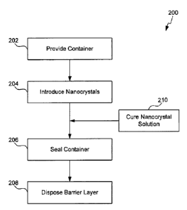
[0012] Figure 2 shows a method for hermetically sealing a container
comprising luminescent nanocrystals in accordance with one embodiment of
the present invention.
[0013] Figure 3 shows hermetically sealed luminescent nanocrystal
compositions, including individually sealed compositions, in accordance with
one embodiment of the present invention.
[0014] Figure 4 shows a hermetically sealed container comprising
luminescent
nanocrystals in accordance with one embodiment of the present invention.
[0015] Figure 5 shows a hermetically sealed composition further
comprising a
microlens in accordance with one embodiment of the present invention.
CA 02678798 2009-08-19
WO 2008/115498
PCT/US2008/003549
-4-
100161 Figures 6A-6C show a hermetically sealed composition further
comprising a light-focusing apparatus in accordance with one embodiment of
the present invention.
[0017] The present invention will now be described with reference to the
accompanying drawings. In the drawings, like reference numbers indicate
identical or functionally similar elements.
DETAILED DESCRIPTION OF THE INVENTION
[0018] It should be appreciated that the particular implementations shown
and
described herein are examples of the invention and are not intended to
otherwise limit the scope of the present invention in any way. Indeed, for the
sake of brevity, conventional electronics, manufacturing, semiconductor
devices, and nanocrystal, nanowire (NW), nanorod, nanotube, and nanoribbon
technologies and other functional aspects of the systems (and components of
the individual operating components of the systems) may not be described in
detail herein.
[0019] The present invention provides various compositions comprising
nanocrystals, including luminescent nanocrystals. The various properties of
the luminescent nanocrystals, including their absorption properties, emission
properties and refractive index properties, can be tailored and adjusted for
various applications. As used herein, the term "nanocrystal" refers to
nanostructures that are substantially monocrystalline. A nanocrystal has at
least one region or characteristic dimension with a dimension of less than
about 500 nm, and down to on the order of less than about 1 nm. As used
herein, when referring to any numerical value, "about" means a value of 10%
of the stated value (e.g. "about 100 nm" encompasses a range of sizes from 90
nm to 110 nm, inclusive). The terms "nanocrystal," "nanodot," "dot" and
"quantum dot" are readily understood by the ordinarily skilled artisan to
represent like structures and are used herein interchangeably. The present
invention also encompasses the use of polycrystalline or amorphous
CA 02678798 2014-08-25
- 5 -
nanocrystals. As used herein, the term "nanocrystal" also encompasses
"luminescent nanocrystals." As used herein, the term "luminescent
nanocrystals"
means nanocrystals that emit light when excited by an external energy source
(suitably light). As used herein when describing the hermetic sealing of
nanocrystals, it should be understood that in suitable embodiments, the
nanocrystals are luminescent nanocrystals.
[0020] Typically, the region of characteristic dimension will be along the
smallest
axis of the structure. Nanocrystals can be substantially homogenous in
material
properties, or in certain embodiments, can be heterogeneous. The optical
properties of nanocrystals can be determined by their particle size, chemical
or
surface composition. The ability to tailor the luminescent nanocrystal size in
the
range between about 1 nm and about 15 nm enables photoemission coverage in
the entire optical spectrum to offer great versatility in color rendering.
Particle
encapsulation offers robustness against chemical and UV deteriorating agents.
[0021] Nanocrystals, including luminescent nanocrystals, for use in the
present
invention can be produced using any method known to those skilled in the art.
Suitable methods and exemplary nanocrystals are disclosed in U.S. Patent No.
7,374,807, issued May 20, 2008; and U.S. Patent No. 6,949,206. The
nanocrystals
for use in the present invention can be produced from any suitable material,
including an inorganic material, and more suitably an inorganic conductive or
semiconductive material. Suitable semiconductor materials include any type of
semiconductor, including group II-VI, group III-V, group IV-VI and group IV
semiconductors. Suitable semiconductor materials include, but are not limited
to,
Si, Ge, Sn, Se, Te, B, C (including diamond), P, BN, BP, BAs, AIN, AIP, AlAs,
AlSb, GaN, GaP, GaAs, GaSb, InN, InP, InAs, InSb, AIN, AlP, AlAs, AlSb,
GaN, GaP, GaAs, GaSb, ZnO, ZnS, ZnSe, ZnTe, CdS, CdSe, CdTe, HgS, HgSe,
HgTe, BeS, BeSe, BeTe, MgS, MgSe, GeS, GeSe, GeTe, SnS, SnSe, SnTe, Pb0,
PbS, PbSe, PbTe, CuF, CuCl, CuBr, CuI, Si3N4, Ge3I\14, A1203, (Al, Ga, In)2
(S,
Se, Te)3, Al2CO, and an appropriate combination of two or more such
semiconductors.
CA 02678798 2014-08-25
- 6 -
[0022] In certain aspects, the semiconductor nanocrystals may comprise a
dopant
from the group consisting of: a p-type dopant or an n-type dopant. The
nanocrystals useful in the present invention can also comprise II-VI or III-V
semiconductors. Examples of II-VI or III-V semiconductor nanocrystals include
any combination of an element from Group II, such as Zn, Cd and Hg, with any
element from Group VI, such as S, Se, Te, Po, of the Periodic Table; and any
combination of an element from Group III, such as B, Al, Ga, In, and T1, with
any
element from Group V, such as N, P, As, Sb and Bi, of the Periodic Table.
[0023] The nanocrystals, including luminescent nanocrystals, useful in
the present
invention can also further comprise ligands conjugated, cooperated, associated
or
attached to their surface as described throughout. Suitable ligands include
any
group known to those skilled in the art, including those disclosed in U.S.
Patent
No. 7,374,807 and U.S. Patent No. 6,949,206. Use of such ligands can enhance
the ability of the nanocrystals to incorporate into various solvents and
matrixes,
including polymers. Increasing the miscibility (i.e., the ability to be mixed
without separation) of the nanocrystals in various solvents and matrixes
allows
them to be distributed throughout a polymeric composition such that the
nanocrystals do not aggregate together and therefore do not scatter light.
Such
ligands are described as "miscibility-enhancing" ligands herein.
[0024] As used herein, the term nanocomposite refers to matrix materials
comprising nanocrystals distributed or embedded therein. Suitable matrix
materials can be any material known to the ordinarily skilled artisan,
including
polymeric materials, organic and inorganic oxides. Nanocomposites of the
CA 02678798 2009-08-19
WO 2008/115498
PCT/US2008/003549
- 7 -
present invention can be layers, encapsulants, coatings or films as described
herein. It should be understood that in embodiments of the present invention
where reference is made to a layer, polymeric layer, matrix, or nanocomposite,
these terms are used interchangeably, and the embodiment so described is not
limited to any one type of nanocomposite, but encompasses any matrix
material or layer described herein or known in the art.
Down-converting nanocomposites (for example, as disclosed in
U.S. Patent Application No. 11/034,216) utilize the emission properties of
luminescent nanocrystals that are tailored to absorb light of a particular
wavelength and then emit at a second wavelength, thereby providing enhanced
performance and efficiency of active sources (e.g., LEDs). As discussed
above, use of luminescent nanocrystals in such down-conversion applications,
as well as other filtering or coating applications, often exposes the
nanocrystals to elevated temperatures, high intensity light (e.g., an LED
source), external gasses, and moisture. Exposure to these conditions can
reduce the efficiency of the nanocrystals, thereby reducing useful product
lifetime. In order to overcome this problem, the present invention provides
methods for hermetically sealing luminescent nanocrystals, as well as
hermetically sealed containers and compositions comprising luminescent
nanocrystals.
Luminescent Nanocrystal Phosphors
[0025] While any method known to the ordinarily skilled artisan can be
used
to create nanocrystal phosphors, suitably, a solution-phase colloidal method
for controlled growth of inorganic nanomaterial phosphors is used. See
Alivisatos, A.P., "Semiconductor clusters, nanocrystals, and quantum dots,"
Science 271:933 (1996); X. Peng, M. Schlamp, A. Kadavanich, A.P.
Alivisatos, "Epitaxial growth of highly luminescent CdSe/CdS Core/Shell
nanocrystals with photostability and electronic accessibility," J. Am. Chem.
Soc. 30:7019-7029 (1997); and C. B. Murray, D.J. Norris, M.G. Bawendi,
"Synthesis and characterization of nearly monodisperse CdE (E = sulfur,
CA 02678798 2014-08-25
- 8 -
selenium, tellurium) semiconductor nanocrystallites," 1 Am. Chem. Soc.
115:8706 (1993). This manufacturing process technology leverages low cost
processability without the need for clean rooms and expensive manufacturing
equipment. In these methods, metal precursors that undergo pyrolysis at high
temperature are rapidly injected into a hot solution of organic surfactant
molecules. These precursors break apart at elevated temperatures and react to
nucleate nanocrystals. After this initial nucleation phase, a growth phase
begins
by the addition of monomers to the growing crystal. The result is freestanding
crystalline nanoparticles in solution that have an organic surfactant molecule
coating their surface.
[0026] Utilizing this approach, synthesis occurs as an initial nucleation
event that
takes place over seconds, followed by crystal growth at elevated temperature
for
several minutes. Parameters such as the temperature, types of surfactants
present,
precursor materials, and ratios of surfactants to monomers can be modified so
as
to change the nature and progress of the reaction. The temperature controls
the
structural phase of the nucleation event, rate of decomposition of precursors,
and
rate of growth. The organic surfactant molecules mediate both solubility and
control of the nanocrystal shape. The ratio of surfactants to monomer,
surfactants
to each other, monomers to each other, and the individual concentrations of
monomers strongly influence the kinetics of growth.
[0027] In suitable embodiments, CdSe is used as the nanocrystal material,
in one
example, for visible light down-conversion, due to the relative maturity of
the
synthesis of this material. Due to the use of a generic surface chemistry, it
is also
possible to substitute non-cadmium-containing nanocrystals.
Core/Shell Luminescent Nanocrystals
[0028] In semiconductor nanocrystals, photo-induced emission arises from
the
band edge states of the nanocrystal. The band-edge emission from luminescent
nanocrystals competes with radiative and non-radiative decay
CA 02678798 2009-08-19
WO 2008/115498
PCT/US2008/003549
- 9 -
channels originating from surface electronic states. X. Peng, et al., J. Am.
Chem. Soc. 30:7019-7029 (1997). As a result, the presence of surface defects
such as dangling bonds provide non-radiative recombination centers and
contribute to lowered emission efficiency. An efficient and permanent method
to passivate and remove the surface trap states is to epitaxially grow an
inorganic shell material on the surface of the nanocrystal. X. Peng, et al.,
J.
Am. Chem. Soc. 30:7019-7029 (1997). The shell material can be chosen such
that the electronic levels are type I with respect to the core material (e.g.,
with
a larger bandgap to provide a potential step localizing the electron and hole
to
the core). As a result, the probability of non-radiative recombination can be
reduced.
[0029] Core-shell structures are obtained by adding organometallic
precursors
containing the shell materials to a reaction mixture containing the core
nanocrystal. In this case, rather than a nucleation-event followed by growth,
the cores act as the nuclei, and the shells grow from their surface. The
temperature of the reaction is kept low to favor the addition of shell
material
monomers to the core surface, while preventing independent nucleation of
nanocrystals of the shell materials. Surfactants in the reaction mixture are
present to direct the controlled growth of shell material and ensure
solubility.
A uniform and epitaxially grown shell is obtained when there is a low lattice
mismatch between the two materials. Additionally, the spherical shape acts to
minimize interfacial strain energy from the large radius of curvature, thereby
preventing the formation of dislocations that could degrade the optical
properties of the nanocrystal system.
[0030] Exemplary materials for preparing core-shell luminescent
nanocrystals
include, but are not limited to, Si, Ge, Sn, Se, Te, B, C (including diamond),
P,
Co, Au, BN, BP, BAs, AIN, AlP, AlAs, AlSb, GaN, GaP, GaAs, GaSb, InN,
InP, InAs, InSb, A1N, AlP, AlAs, AlSb, GaN, GaP, GaAs, GaSb, ZnO, ZnS,
ZnSe, ZnTe, CdS, CdSe, CdTe, HgS, HgSe, HgTe, BeS, BeSe, BeTe, MgS,
MgSe, GeS, GeSe, GeTe, SnS, SnSe, SnTe, Pb0, PbS, PbSe, PbTe, CuF,
CuCl, CuBr, CuI, Si3N4, Ge3N4, A1203, (Al, Ga, In)2 (S, Se, Te)3, Al2CO, and
CA 02678798 2009-08-19
WO 2008/115498
PCT/US2008/003549
- 10 -
an appropriate combination of two or more such materials. Exemplary core-
shell luminescent nanocrystals for use in the practice of the present
invention
include, but are not limited to, (represented as Core/Shell), CdSe/ZnS,
1nP/ZnS, PbSe/PbS, CdSe/CdS, CdTe/CdS, CdTe/ZnS, as well as others.
Hermetically Sealed Luminescent Nanocrystal Compositions and Luminescent
Nanocrystal-comprising Containers
[0031] In one embodiment, the present invention provides methods of
hermetically sealing a composition comprising a plurality of luminescent
nanocrystals. The methods suitably comprise disposing a barrier layer on the
composition to seal the luminescent nanocrystals. As discussed throughout,
the terms "hermetic," "hermetic sealing," and "hermetically sealed" are used
throughout to indicate that the composition, container and/or luminescent
nanocrystals are prepared in such a way that the quantity of gases (e.g., air)
or
moisture that passes through or penetrates the container or composition,
ancVor
that contacts the luminescent nanocrystals is reduced to a level where it does
not substantially effect the performance of the nanocrystals (e.g., their
luminescence). Therefore, a "hermetically sealed composition," for example
one that comprises luminescent nanocrystals, is a composition that does not
allow an amount of air (or other gas, liquid or moisture) to penetrate the
composition and contact the luminescent nanocrystals such that the
performance of the nanocrystals (e.g., the luminescence) is substantially
effected or impacted (e.g., reduced).
[0032] As used throughout, a plurality of luminescent nanocrystals
means
more than one nanocrystal (i.e., 2, 3, 4, 5, 10, 100, 1,000, 1,000,000, etc.,
nanocrystals). The
compositions will suitably comprise luminescent
nanocrystals having the same composition, though in further embodiments, the
plurality of luminescent nanocrystals can be various different compositions.
For example, the luminescent nanocrystals can all emit at the same
wavelength, or in further embodiments, the compositions can comprise
luminescent nanocrystals that emit at different wavelengths.
CA 02678798 2009-08-19
WO 2008/115498 PC
T/US2008/003549
- 11 -
[0033] As shown in Figure 1, in one embodiment, the present invention
provides a composition 100 comprising a plurality of luminescent nanocrystals
104. Any nanocrystal can be prepared in the compositions of the present
invention, including those described throughout, and otherwise known in the
art, for example, as disclosed in U.S. Patent Application No. 11/034,216.
[0034] In suitable embodiments, composition 100 comprises a plurality of
luminescent nanocrystals 104 dispersed throughout a matrix 102. As used
throughout, dispersed includes uniform (i.e., substantially homogeneous) as
well as non-uniform (i.e., substantially heterogeneous) distribution/placement
of nanocrystals. Suitable matrixes for use in the compositions of the present
invention include polymers and organic and inorganic oxides. Suitable
polymers for use in the matrixes of the present invention include any polymer
known to the ordinarily skilled artisan that can be used for such a purpose.
In
suitable embodiments, the polymer will be substantially translucent or
substantially transparent. Such polymers include, but are not limited to,
poly(vinyl butyral):poly(vinyl acetate); epoxies; urethanes; silicone and
derivatives of silicone, including, but not limited to,
polyphenylmethylsiloxane, polyphenylalkylsiloxane, polydiphenylsiloxane,
polydialkylsiloxane, fluorinated silicones and vinyl and hydride substituted
silicones; acrylic polymers and copolymers formed from monomers including
but not limited to, methylmethacrylate, butylmethacrylate and
laurylmethacrylate; styrene based polymers; and polymers that are crosslinked
with difunctional monomers, such as divinylbenzene.
[0035] The luminescent nanocrystals used the present invention can be
embedded in a polymeric (or other suitable material, e.g., waxes, oils) matrix
using any suitable method, for example, mixing the nanocrystals in a polymer
and casting a film, mixing the nanocrystals with monomers and polymerizing
them together, mixing the nanocrystals in a sol-gel to form an oxide, or any
other method known to those skilled in the art. As used herein, the term
"embedded" is used to indicate that the luminescent nanocrystals are enclosed
or encased within the polymer that makes up the majority component of the
CA 02678798 2009-08-19
WO 2008/115498
PCT/US2008/003549
- 12 -
matrix. It should be noted that luminescent nanocrystals are suitably
uniformly distributed throughout the matrix, though in further embodiments
they can be distributed according to an application-specific uniformity
distribution function.
[0036] The thickness of the composition of the present invention can be
controlled by any method known in the art, such as spin coating and screen
printing. The luminescent nanocrystal compositions of the present invention
can be any desirable size, shape, configuration and thickness. For example,
the compositions can be in the form of layers, as well as other shapes, for
example, discs, spheres, cubes or blocks, tubular configurations and the like.
While the various compositions of the present invention can be any thickness
required or desired, suitably, the compositions are on the order of about
100 mm in thickness (i.e., in one dimension), and down to on the order of less
than about 1 mm in thickness. In other embodiments, the polymeric layers of
the present invention can be on the order of 10's to 100's of microns in
thickness. The luminescent nanocrystals can be embedded in the various
compositions/matrixes at any loading ratio that is appropriate for the desired
function. Suitably, the luminescent nanocrystals will be loaded at a ratio of
between about 0.001% and about 75% by volume depending upon the
application, matrix and type of nanocrystals used. The appropriate loading
ratios can readily be determined by the ordinarily skilled artisan and are
described herein further with regard to specific applications. In exemplary
embodiments the amount of nanocrystals loaded in a luminescent nanocrystal
composition are on the order of about 10% by volume, to parts-per-million
(ppm) levels.
[0037] Luminescent nanocrystals for use in the present invention will
suitably
be less than about 100 nm in size, and down to less than about 2 nm in size.
In suitable embodiments, the luminescent nanocrystals of the present invention
absorb visible light. As used herein, visible light is electromagnetic
radiation
with wavelengths between about 380 and about 780 nanometers that is visible
to the human eye. Visible light can be separated into the various colors of
the
CA 02678798 2009-08-19
WO 2008/115498
PCT/US2008/003549
- 13 -
spectrum, such as red, orange, yellow, green, blue, indigo and violet. The
photon-filtering nanocomposites of the present invention can be constructed so
as to absorb light that makes up any one or more of these colors. For example,
the nanocomposites of the present invention can be constructed so as to absorb
blue light, red light, or green light, combinations of such colors, or any
colors
in between. As used herein, blue light comprises light between about 435 nm
and about 500 nm, green light comprises light between about 520 nm and
565 nm and red light comprises light between about 625 nm and about 740 nm
in wavelength. The ordinarily skilled artisan will be able to construct
nanocomposites that can filter any combination of these wavelengths, or
wavelengths between these colors, and such nanocomposites are embodied by
the present invention.
[0038] In other embodiments, the luminescent nanocrystals have a size and
a
composition such that they absorb photons that are in the ultraviolet, near-
infrared, and/or infrared spectra. As used herein, the ultraviolet spectrum
comprises light between about 100 nm to about 400 nm, the near-infrared
spectrum comprises light between about 750 nm to about 100 1.tm in
wavelength and the infrared spectrum comprises light between about 750 nm
to about 300 m in wavelength.
[0039] While luminescent nanocrystals of any suitable material can be
used in
the practice of the present invention, in certain embodiments, the
nanocrystals
can be ZnS, InAs or CdSe nanocrystals, or the nanocrystals can comprise
various combinations to form a population of nanocrystals for use in the
practice of the present invention. As discussed above, in further embodiments,
the luminescent nanocrystals are core/shell nanocrystals, such as CdSe/ZnS,
CdSe/CdS or InP/ZnS.
[0040] In order to hermetically seal the compositions of the present
invention,
a barrier layer is disposed on the composition. For example, as shown in
Figure 1, a barrier layer 106 is disposed on the matrix 102 comprising
luminescent nanocrystals 104, thereby generating a hermetically sealed
composition. The term "barrier layer" is used throughout to indicate a layer,
CA 02678798 2014-08-25
- 14 -
coating, sealant or other material that is disposed on the matrix 102 so as to
hermetically seal the composition. Examples of barrier layers include any
material
layer, coating or substance that can create an airtight seal on the
composition.
Suitable barrier layers include inorganic layers, suitably an inorganic oxide
such
as an oxide of Al, Ba, Ca, Mg, Ni, Si, Ti or Zr. Exemplary inorganic oxide
layers,
include Si02, Ti02, A102 and the like. As used throughout, the terms
"dispose,"
and "disposing" include any suitably method of application of a barrier layer.
For
example, disposing includes layering, coating, spraying, sputtering, plasma
enhanced chemical vapor deposition, atomic layer deposition, or other suitable
method of applying a barrier layer to the compositions. In suitable
embodiments,
sputtering is used to dispose the barrier layer on the compositions.
Sputtering
comprises a physical vapor deposition process where high-energy ions are used
to
bombard elemental sources of material, which eject vapors of atoms that are
then
deposited in thin layers on a substrate. See for example, U.S. Patent Nos.
6,541,790; 6,107,105; and 5,667,650.
[0041] In further embodiments, disposing the barrier layer can be carried
out
using atomic layer deposition, in applications such as coatings of LEDs,
luminescent nanocrystal compositions, such as nanocrystal-comprising polymeric
layers, can often have complex geometries and features. For example,
components of the LED such as bond wires and solder joints often are directly
in
contact with, or even contained within, the polymeric layer, in order to
properly
hermetically seal the nanocrystal composition, a virtually defect-free (i.e.,
pin
hole-free) barrier layer is often required. In addition, application of the
barrier
layer should not degrade the polymer or the nanocrystals. Therefore, in
suitable
embodiments, atomic layer deposition is used to dispose the barrier layer.
[0042] Atomic layer deposition (ALD) can comprise disposition of an oxide
layer
(e.g., Ti02, Si02, A102, etc.) on the luminescent nanocrystal composition, or
in
further embodiments, deposition of a non-conductive layer,
CA 02678798 2009-08-19
WO 2008/115498
PCT/US2008/003549
- 15 -
such as a nitride (e.g., silicon nitride) can be used. ALD deposits an atomic
layer (i.e., only a few molecules thick) by alternately supplying a reaction
gas
and a purging gas. A thin coating having a high aspect ratio, uniformity in a
depression, and good electrical and physical properties, can be formed.
Barrier layers deposited by the ALD method suitably have a low impurity
density and a thickness of less than 1000 nm, suitably less than about 500 nm,
less than about 200 nm, less than about 50 nm, less than about 20 nm, or less
than about 5 nm.
[0043] For example, in suitable embodiments, two reaction gases, A and B
are
used. When only the reaction gas, A, flows into a reaction chamber, atoms of
the reaction gas A are chemically adsorbed on the luminescent nanocrystal
composition. Then, any remaining reaction gas A is purged with an inert gas
such as Ar or nitrogen. Then, reaction gas B flows in, wherein a chemical
reaction between the reaction gases A and B occurs only on the surface of the
luminescent nanocrystal composition on which the reaction gas A has been
adsorbed, resulting in an atomic barrier layer on the composition.
[0044] In embodiments where a non-conductive layer, such as a nitride
layer
is disposed, suitably SiH2C12 and remote plasma enhanced NH3 are used to
dispose a silicon nitride layer. This can be performed at a low temperature
and does not require the use of reactive oxygen species.
[0045] Use of ALD for disposition of a barrier layer on the luminescent
nanocrystal composition generates a virtually pin-hole free barrier layer
regardless of the morphology of the substrate. The thickness of the barrier
layer can be increased by repeating the deposition steps, thereby increasing
the
thickness of the layer in atomic layer units according to the number of
repetitions. In addition, the barrier layer can be further coated with
additional
layers (e.g., via sputtering, CVD or ALD) to protect or further enhance the
barrier.
[0046] Suitably, the ALD methods utilized in the practice of the present
invention are performed at a temperature of below about 500 C, suitably
below about 400 C, below about 300 C, or below about 200 C.
CA 02678798 2009-08-19
WO 2008/115498
PCT/US2008/003549
- 16 -
[0047]
Exemplary barrier materials include organic material designed to
specifically reduce oxygen and moisture transmission. Examples include
filled epoxies (such as alumina filled epoxies) as well as liquid crystalline
polymers.
[0048] As discussed throughout, matrix 102 suitably comprises a
polymeric
substrate. Thus, the present invention comprises methods of hermetically
sealing compositions comprising luminescent nanocrystals, suitably polymeric
substrates comprising luminescent nanocrystals, by disposing a barrier layer
on the composition using any of the various methods disclosed herein or
otherwise known in the art..
[0049] The ability to use polymeric substrates as matrix 102 allows for
the
formation of various shapes and configurations of the compositions, simply by
molding or otherwise manipulating the compositions into the desired
shape/orientation. For
example, a solution/suspension of luminescent
nanocrystals can be prepared (e.g., luminescent nanocrystals in a polymeric
matrix). This solution can then be placed into any desired mold to form a
required shape, and then cured (e.g., cooled or heated depending upon the type
of polymer) to form a solid or semi-solid structure. For example, a mold can
be prepared in the shape of a cap or disc to place on or over an LED. This
then allows for preparation of a composition that can be used as a down-
converting layer, for example. Following preparation of the desired shape, a
barrier layer is then disposed on the composition to hermetically seal the
composition, thereby protecting the luminescent nanocrystals from oxidation.
[0050] In additional embodiments, a composition comprising luminescent
nanocrystals (e.g., a polymeric composition) can be disposed directly on a
desired substrate or article (for example an LED). The luminescent
nanocrystal composition (e.g., a solution or suspension) can then be cured and
then a barrier layer disposed on the composition, thereby hermetically sealing
the composition directly on the desired substrate or article. Such embodiments
therefore do not require the preparation of a separate composition, and
instead
CA 02678798 2009-08-19
WO 2008/115498
PCT/US2008/003549
- 17 -
allow for the preparation of the composition directly on the desired
article/substrate (e.g., a light source or other end product).
[0051] In a further embodiment, the present invention provides methods
for
hermetically sealing a container which comprises a plurality of luminescent
nanocrystals. Suitably
the methods comprise providing a container,
introducing luminescent nanocrystals into the container, and then sealing the
container. For example, an exemplary method for hermetically sealing a
container of luminescent nanocrystals is shown in flowchart 200 of Figure 2,
with reference to Figures 3 and 4. In step 202 if Figure 2, a container is
provided, for example, containers 302 or 402 in Figures 3 and 4 are be
provided. As used herein, "container" refers to any suitable article or
receptacle for retaining nanocrystals. It should be understood that, as used
herein, a "container" comprising luminescent nanocrystals and a
"composition" comprising luminescent nanocrystals represent different
embodiments of the present invention. A
"composition" comprising
luminescent nanocrystals refers to a matrix, e.g., a polymer substrate,
solution
or suspension, which contains nanocrystals dispersed throughout. A
"container" as used herein, refers to a carrier, receptacle or pre-formed
article
into which luminescent nanocrystals are introduced (often a composition of
luminescent nanocrystals, e.g., a polymeric matrix comprising luminescent
nanocrystals). Examples of containers include, but are not limited to,
polymeric or glass structures such as tubes, molded or formed vessels, or
receptacles. In exemplary embodiments, a container can be formed by
extruding a polymeric or glass substance into a desired shape, such as a tube
(circular, rectangular, triangular, oval or other desired cross-section), or
similar structure. Any polymer can be used to form the containers for use in
the practice of the present invention, including those described throughout.
Exemplary polymers for preparation of containers for use in the practice of
the
present invention include, but are not limited to, acrylics, poly(methyl
methacrylate) (PMIVIA), and various silicone derivatives. Additional materials
can also be used to form the containers for use in the practice of the present
CA 02678798 2009-08-19
WO 2008/115498
PCT/US2008/003549
- 18 -
invention. For example, the containers can be prepared from metals, various
glasses, ceramics and the like.
[0052] For example, as shown in Figure 2, once a container is provided in
step
202, a plurality of luminescent nanocrystals 104 are then introduced into the
container in step 204. As used herein, "introduced" includes any suitable
method of providing luminescent nanocrystals into a container. For example,
luminescent nanocrystals can be injected into a container, placed into a
container, drawn into a container (e.g., by using a suction or vacuum
mechanism), directed into a container, for example by using an
electromagnetic field, or other suitable method for introducing luminescent
nanocrystals into a container. Suitably, the luminescent nanocrystals are
present in a solution or suspension, for example in a polymeric solution,
thereby aiding in the introduction of the nanocrystals into the container. In
exemplary embodiments, luminescent nanocrystals 104 can be drawn into a
container, for example a tubular container 302, such as is shown in Figure 3.
In further embodiments, as shown in Figure 4, a container 402 can be prepared
with a cavity or void 404 into which luminescent nanocrystals 104 can be
introduced. For example, a solution of luminescent nanocrystals 104 can be
introduced into the cavity 404 in container 402.
[0053] Following introduction of the luminescent nanocrystals into the
container, the container is then hermetically sealed, as shown in Figure 2, in
step 206. Examples of methods for hermetically sealing the container include,
but are not limited to, heat sealing the container, ultrasonic welding the
container, soldering the container or adhesive bonding the container. For
example, as shown in Figure 3, container 302 can be sealed at any number of
positions, creating various number of seals 304 throughout the container. In
exemplary embodiments, container 302 can be heat sealed at various positions
throughout the container, for example by heating and then "pinching" the
container at various sealing points (304).
[0054] In suitable embodiments, as shown in Figure 3, a polymeric or
glass
tube can be used as container 302. A solution of luminescent nanocrystals 104
CA 02678798 2009-08-19
WO 2008/115498
PCT/US2008/003549
- 19 -
can then be drawn into the container by simply applying a reduced pressure to
an end of the container. Container 302 can then be sealed by heating and
"pinching" the container at various sealing positions or seals 304 throughout
the length of the container, or by using other sealing mechanisms as described
throughout. In this way, container 302 can be separated into various
individual sections 306. These sections can either retained together as a
single, sealed container 308, or the sections can be separated into individual
pieces, as shown in Figure 3. Hermetic sealing of container 302 can be
performed such that each individual seal 304 separates solutions of the same
nanocrystals. In other embodiments, seals 304 can be created such that
separate sections of container 302 each contain a different nanocrystal
solution
(i.e., different nanocrystal composition, size or density).
[0055] In a further embodiment, as shown in Figure 4, luminescent
nanocrystals can be placed into a cavity/void 404 formed in container 402.
Container 402 can be produced using any suitable process. For example,
container 402 can be injection molded into any desired shape or configuration.
Cavity/void 404 can be prepared during the initial preparation process (i.e.,
during molding) or can be subsequently added after formation. Luminescent
nanocrystals 104 are then introduced into cavity/void 404. For example,
luminescent nanocrystals can be injected or placed into cavity/void 404 of
container 402. Suitably, a solution of luminescent nanocrystals will fill the
entire container, though it is not necessary to completely fill the container
with
nanocrystals. In the case where the entire container is not filled, it is
necessary
though to remove substantially all of the air in the container prior to
sealing to
ensure that the luminescent nanocrystals are hermetically sealed. As shown in
Figure 4, in exemplary embodiments, container 402 can be hermetically sealed
by bonding, welding or otherwise sealing the container with a cover or lid
406.
Suitably, cover 406 is produced from the same material as container 402 (and
can suitably be partially attached prior to sealing), though it can also
comprise
a different material. In additional embodiments, a material such as an organic
material designed to specifically reduce oxygen and moisture transmission can
CA 02678798 2009-08-19
WO 2008/115498
PCT/US2008/003549
- 20 -
be used to cover or seal container 402. Examples include filled epoxies (such
as alumina filled epoxies) as well as liquid crystalline polymers.
[0056] The ability to produce custom designed containers, for example via
molding, extruding or otherwise shaping containers, allows for preparation of
very specialized parts into which luminescent nanocrystals can be introduced
and hermetically sealed. For example, shapes can be produced that conform
around LEDs or other light sources (e.g., for use to pipe down-conversion into
another optical component). In addition, various films, discs, layers, and
other
shapes can be prepared. In exemplary embodiments, several different
containers can be prepared, each of which can contain different compositions
of luminescent nanocrystals (i.e., each composition emitting a different
color),
and then the separate containers can be utilized together to create the
desired
performance characteristics. In further embodiments, containers can be
prepared with multiple cavities or reservoirs into which luminescent
nanocrystals can be introduced.
[0057] While luminescent nanocrystals 104 can be hermetically sealed into
containers 302, 402, while still in solution, suitably the luminescent
nanocrystal solution is cured before hermetic sealing (e.g., in step 210 of
Figure 2). As used herein, "cured" refers to the process of hardening a
solution of luminescent nanocrystals (e.g., a polymeric solution). Curing can
be achieved by simply allowing the solution to dry and any solvent to
evaporate, or curing can be achieve by heating or exposing the solution to
light
or other external energy. Following curing, the container can be hermetically
sealed using the various methods described throughout.
[0058] In exemplary embodiments, no additional hermetic sealing is
necessary
to protect the luminescent nanocrystals from oxidative degradation. For
example, sealing luminescent nanocrystals in a glass or polymeric container
provides sufficient protection from oxygen and moisture that further
modifications are not necessary. However, in further embodiments, an
additional level of protection from oxidation can be added to the hermetically
sealed containers by disposing a barrier layer on the container. For example,
CA 02678798 2009-08-19
WO 2008/115498
PCT/US2008/003549
- 21 -
as shown in step 208 of Figure 2. As described throughout, exemplary barrier
layers include inorganic layers, such as inorganic oxides like Si02, TiO2 and
A102, as well as organic materials. While any method of disposing the barrier
layer onto the container can be used, suitably the barrier layer is sputtered
onto
the container or disposed onto the container via ALD. As shown in Figure 3,
barrier layer 106 can be disposed on the container with sealed sections, or on
individual sections following sealing and separation from one another, thereby
producing hermetically sealed containers (310, 312).
[0059] In suitable embodiments of the present invention, the various
steps to
produce a hermetically sealed container of luminescent nanocrystals are
performed in an inert atmosphere. For example, steps 204, 206 and 208 (and
210 if required) are all suitably performed in an inert atmosphere, i.e.,
either in
a vacuum and/or with only N2 or other inert gas(es) present.
[0060] In further embodiments, the present invention provides
hermetically
sealed compositions and containers comprising a plurality of luminescent
nanocrystals. In exemplary embodiments, the luminescent nanocrystals
comprise one or more semiconductor materials (as described throughout), and
are suitably core/shell luminescent nanocrystals, such as CdSe/ZnS, CdSe/CdS
or InP/ZnS. In general, the luminescent nanocrystals are of a size of between
about 1-50 nm, suitably about 1-30 nm, more suitably about 1-10 nm, e.g.,
about 3-9 nm. In exemplary embodiments, as described throughout, the
hermetically sealed compositions and containers of the present invention
comprise a barrier layer coating the composition (e.g., barrier layer 106
coating composition 100 in Figure 1) and optionally comprise a barrier layer
coating the containers (e.g., barrier layer 106 coating container 302 in
Figure
3). Exemplary types of barrier layers include those described throughout, such
as inorganic layers like Si02, Ti02, and A102.
[0061] In addition to generating various shapes, orientations and sizes
of
containers for hermetically sealing the luminescent nanocrystals, additional
modifications can also be made to the containers/compositions. For example,
the containers/compositions can be prepared in the shape of a lens for
filtration
CA 02678798 2009-08-19
WO 2008/115498
PCT/US2008/003549
- 22 -
or other modification of a light source. In further embodiments, the
containers/compositions can be modified, for example, by preparing or
attaching a reflector or similar apparatus to the containers/compositions.
[0062] Additionally, micropatterns can be molded directly into the
compositions or containers to form flat (or curved) microlenses. This can be
done during the molding process or in a subsequent embossing step.
Micropatterns are often utilized to make flat microlenses when limited space
is
available, such as in displays. Examples of this technology include the
brightness enhancing films from 3M corporation that have 20 to 50 micron
prisms molded into their surface. In suitable embodiments, the present
invention provides microlenses comprising luminescent nanocrystals
hermetically sealed in an encapsulating polymer (or in a container) which is
then micropatterned such that a microlens is formed. For example, as shown
in Figure 5, microlens assembly 500 suitably comprises hermetically sealed
composition 502 comprising a layer 504 of luminescent nanocrystals 104
placed on top of, or otherwise in contact with, LED 506 which is supported by
substrate 508. The surface of composition 502 can be molded into various
shapes, for example to include a series of microprisms 510, as shown in Figure
5, thereby forming the microlens.
[0063] In exemplary embodiments, use of a microlens in combination with
the
hermetically sealed compositions of the present invention allow for an
increase in the amount of emitted light captured (and therefore emitted from
the composition) from the LED/luminescent nanocrystals. For example, the
addition of microprisms or other microlens assembly to the hermetically
sealed compositions and containers of the present invention suitably leads to
an increase in the amount of light captured of greater than about 10% (e.g.,
about 10-60%, about 10-50%, about 10-40%, about 20%-40%, or about 30-
40%) as compared to a composition that does not comprise microprisms or
other microlens assembly. This increase in the amount of light captured
correlates directly to an increase in the total amount of light that is
emitted
from the composition or container.
CA 02678798 2014-08-25
- 23 -
[0064] In suitable embodiments, a dichroic mirror can be attached or
otherwise
associated with the containers/compositions that forms a lens for application
over
a light source. A dichroic mirror allows a particular wavelength of light to
pass
through the mirror, while reflecting others. As light from the source enters
the
lens-shaped containers/compositions, the photons are able to enter the
containers/compositions and excite the various luminescent nanocrystals that
have
been hermetically sealed inside. As the luminescent nanocrystals emit light,
photons are able to exit the containers/compositions, but not reflect back
toward
the initial light source (as they are reflected by the dichroic mirror). In
embodiments then, suitable containers/compositions can be created to fit over
a
light source (e.g., an LED). This allows light to enter from the source and
excite
the luminescent nanocrystals inside, but emitted light is only allowed to exit
the
containers/compositions away from the light source, blocked from reflecting
back
into the source by the dichroic mirror. For example, blue light from an LED
source is allowed to pass through the dichroic mirror and excite encapsulated
luminescent nanocrystals, which then emit green light. The green light is
reflected
by the mirror and not allowed to reflect back into the light source.
[0065] As discussed herein, in suitable embodiments the hermetically
sealed
luminescent nanocrystal compositions of the present invention are used in
combination with an LED or other light source. Applications for these sealed
nanocrystal/LEDs are well known to those of ordinary skill in the art, and
include
the following. For example, such sealed nanocrystal/LEDs can be used in
microprojectors (see, e.g., U.S. Patent No. 7,180,566 and 6,755,563); in
applications such as cellular telephones; personal digital assistants (PDAs);
personal media players; gaming devices; laptops; digital versatile disk (DVD)
players and other video output devices; personal color eyewear; and head-up or
head-down (and other) displays for automobiles and
CA 02678798 2009-08-19
WO 2008/115498
PCT/US2008/003549
- 24 -
airplanes. In additional embodiments, the hermetically sealed nanocrystals
can be used in applications such as digital light processor (DLP) projectors.
[0066] In additional embodiments, the hermetically sealed compositions
and
containers disclosed throughout can be used to minimize the property of an
optical system known as etendue (or how spread out the light is in area and
angle). By disposing, layering or otherwise covering (even partially covering)
an LED or other light source with a composition or container of the presently
claimed invention, and controlling the ratio of the overall area (e.g, the
thickness) of the luminescent nanocrystal composition or container to the area
(e.g., the thickness) of the LED, the amount or extent of etendue can be
minimized, thereby increasing the amount of light captured and emitted.
Suitably, the thickness of the luminescent nanocrystal composition or
container will be less than about 1/5 the thickness of the LED layer. For
example, the luminescent nanocrystal composition or container will be less
than about 1/6, less than about 1/7, less than about 1/8, less than about 1/9,
less than about 1/10, less than about 1/15 or less than about 1/20 of the
thickness of the LED layer.
[0067] In further embodiments, the hermetically sealed luminescent
nanocrystals of the presently claimed invention can be used in a system 602
comprising a light-focusing apparatus (or focusing apparatus) 604, for
example, as shown in FIGs. 6A-6C. In exemplary embodiments, a light-
focusing apparatus 604 is prepared and attached or otherwise associated with
an LED 506. Suitably, light-focusing apparatus 604 is in the shape of a cube
or rectangular box, where the bottom of the box situated on or above the LED
506, with the sides of the apparatus extending above the LED. FIG. 6A shows
a cross sectional view of apparatus 604, taken through plane 1-1 of FIG. 6B,
showing a top view of the apparatus 604, LED 506 and substrate 508. In
exemplary embodiments, apparatus 604 comprises four sides surrounding
LED 506, though in other embodiments any number of sides can be used (e.g.,
2, 3, 4 5, 6, 7, 8, 9, 10, etc.), or a circular apparatus can be used, such
that only
a single piece (or multiple pieces fashioned for form a continuous piece) of
CA 02678798 2009-08-19
WO 2008/115498
PCT/US2008/003549
- 25 -
material surrounds LED 506. In general, the top and bottom of light-focusing
apparatus 604 are open (i.e., the apparatus is placed directly on top of and
encloses LED 506), though in other embodiments, either the top or bottom, or
both, of apparatus 604 can be closed by an additional piece of material.
[0068] Focusing apparatus 604 suitably is made of a material that can
reflect
light that is generated by LED, or is coated with a material that reflects
light.
For example, focusing apparatus can comprise a polymer, metal, ceramic, etc.
In other embodiments, the inner surface (i.e., the surface facing LED) can be
coated with a reflective material such as a metal (e.g, Al) or other
reflective
coating. This reflective coating can be deposited on the surfaces of focusing
apparatus using any suitable method, such as spray coating, ALD, painting,
dipping, spin coating, etc.
[0069] Focusing apparatus 604 suitably encloses or encapsulates a
hermetically sealed nanocrystal composition 504 (or hermetically sealed
nanocrystal container) of the present invention, and thus the apparatus is
associated with the composition or container. In suitable embodiments,
focusing apparatus 604 can be prepared separately from LED 506 and then
attached to the LED, for example by an adhesive such as an epoxy, and then
the center portion of the apparatus 604 filled in with a hermetically sealed
nanocrystal composition 504. In further embodiments, focusing apparatus 604
can be directly assembled on LED 506. In other embodiments, a hermetically
sealed composition can be disposed on LED and then focusing apparatus can
be added, either as a pre-made apparatus, or constructed directly on the LED.
In suitable embodiments, apparatus 604 also comprises a cover (e.g., a glass
or polymer cover) to seal the nanocrystal composition 504. Such a cover can
act as a hermetic seal over the nanocrystal composition, or simply as an
additional structural element to support the nanocrystal composition and the
focusing apparatus. Such a cover can be placed directly on top of nanocrystal
composition 504, or can be placed at the top of apparatus 604, or in any
position in between.
CA 02678798 2015-08-21
-26-
100701 As shown in FIGs 6A and 6C, in suitable embodiments, focusing
apparatus 604 is
prepared in such a manner that the sides of the apparatus taper inward at the
bottom (e.g.,
near the LED), but outward at the top (away from the LED). This helps to aid
in
gathering and focusing the light 606 into a beam so as to direct the light out
of the
apparatus. As shown FIG 6C, suitably focusing apparatus 604 directs light 606
out from
the LED. By using tapered or angled sides, light 606 that is emitted from the
LED/nanocrystals is directed out of the apparatus 604, rather than lost either
by bouncing
back and forth inside of the apparatus, or lost simply unable to escape. Use
of light-
focusing apparatus in combination with the luminescent nanocrystal
compositions and
containers of the present invention can suitably be employed in
microprojectors and other
applications where a focus, beam of light is desired or required.
EXAMPLES
[0071] The following examples are illustrative, but not limiting, of the
method and
compositions of the present invention. Other suitable modifications and
adaptations of the
variety of conditions and parameters normally encountered in nanocrystal
synthesis, and
which would become apparent to those skilled in the art, and are within the
scope of the
invention.
Example 1
Preparation of Hermetically Sealed Containers
[00721 A rectangular tube of approximate dimensions 3 mm x 0.5 mm with a
2 mm x 0.5
mm cavity is prepared by extrusion of PMMA. The length of tubing is then
filled with a
solution comprising fluorescent luminescent nanocrystals. The luminescent
nanocrystal
solution is then cured. Segments of the tubing are then heat sealed to trap
the nanocrystals
in the tubing. Suitably the filling and sealing are performed in an inert
atmosphere. A
barrier layer (e.g., Si02, TiO2 or A102) can then be disposed on the outer
surface of the
tubing.
CA 02678798 2015-08-21
- 27
[0073] A drawn glass capillary can also be used to prepare a hermetically
sealed
container comprising nanocrystals. The end of the capillary is sealed either
via melt
sealing or plugging with a solder or adhesive or similar structure. The
capillary can be
filled with a solution of luminescent nanocrystals such that the entire volume
of the
capillary is filled with the same nanocrystal solution, or the capillary can
be filled in
stages, such that different nanocrystals are separated along the length of the
capillary. For
example, a first luminescent nanocrystal solution can be introduced into the
capillary, and
then a seal placed adjacent to the solution (for example, but melt sealing or
plugging the
capillary). A second luminescent nanocrystal solution can then be added to the
capillary,
and again, a seal placed adjacent to the solution. This process can be
repeated as often as
required until the desired number of individual, hermetically sealed
nanocrystal segments
are created. In this manner, different compositions of luminescent
nanocrystals can be
separated from each other in the same container, thereby allowing the
production of
containers comprising multiple compositions (e.g., colors) of luminescent
nanocrystals.
In a similar embodiment, a multi-lumen capillary can be used in which
different
compositions of luminescent nanocrystals (e.g., those which emit different
colors) can be
introduced and thus kept separate from each other, and still be hermetically
sealed from
external air and moisture.
[0074] Exemplary embodiments of the present invention have been
presented. The
invention is not limited to these examples. These examples are presented
herein for
purposes of illustration, and not limitation. Alternatives (including
equivalents,
extensions, variations, deviations, etc., of those described herein) will be
apparent to
persons skilled in the relevant art(s) based on the teachings contained
herein. Such
alternatives fall within the scope of the invention.