Note: Descriptions are shown in the official language in which they were submitted.
CA 02678878 2009-08-19
WO 2008/103696 PCT/US2008/054365
3-PHASE HIGH-POWER UPS
BACKGROUND OF INVLN'T"ION
Uninterruptible power supplies (UPSs) including voltage converters are fundaa-
nental
parts of many electrical systems such as power supply systems for conlputers
and servers in
data ccnters. UPSs can be used with many typical power systems including
single and 3-pbase
connections, and can be used with low-power systems (e.g., a household
computer) and high-
power systems (e.g., large data centers or process facilities). High-power
systems typically use
a 3-phase power connection (e.g., X, Y, and Z phases). A 3-phase UPS voltage
converter is
typically used to provide 3-phase AC power to a 3-phase load, to convert a 3-
phase AC voltage
from one level to another, and to provide 3-phase power to a load in the event
of a power
failure. The input and output connections to a 3-phase UPS voltage converter
are typicaliy
three- or four-terminal connections, one connection for each phase of the 3-
phase power
connection and an optional neutral connection. A battery is also typically
coupled to the UPS
voltage converter and is used to store energy for use in case of a power
failure.
'T'ypical high powcr (e.g., above 100 kW) UI'Ss are operated using nominaI AC
input
voltages of 3x400 V(in I7urope) or 3x480 V (in the U.S.). 'I'ransl'ormerless
UPSs may operate
with an internal DC bus voltage of +450 V. ln such a configuration, components
contained in
thc tJPS arc preferably rated for at least 1200 V opei-ation due to large
voltage overshoots
associated with stray iziductajiies of physically large insulated gate bipolar
transistor (IGI3'T')
modules, "llae tise of 1200 V components, howevei-, typically ieacis to
iiicreased conduction
and switch.in- Iosses, thus lowei=i.ng the efficieticy.
SliiMMARY OF INV3-;N`1'ION
In I;cnei-aI, in an aspect, the inventioli provides a UPS i.ncluding a
plurality of electrical
buses, a first AC/DC converter coupled to t:he electrical buses and
configuz=ed to i=eceive a first
input AC voltage and to convert the first input AC voltage to a plrai-al'Ãty
of DC volta(Yes, the
first A.C./1;3C, converter beint) configured to convey the plurality of DC
voltages to the plurality
of electrical buses, a second AC/DC converter coupled to the electrical buses
aiad configured to
i-cceive a second input AC voltage and to convert the second input AC voltage
to the plurality
of DC voltages, the secoiid AC/DC convet-tcr being configured to convcy the
plurality of DC
voltages to the plurality of electrical buses, a third AC/DC converter coupled
to the electrical
buses and cof-ifigui-ed to receive a third input AC voltage and to convert the
t}iird input AC.
CA 02678878 2009-08-19
WO 2008/103696 PCT/US2008/054365
-2-
voltage to the plurality of DC voltages, the third AC/DC converter being col-
ifigured to convey
the plurality of DC voltages to the plurality of electrical buses, a DC/DC
convei-ter coupled to
the plurality of electrical buses and configured to, convert the plurality of
DC voltages to a
battery DC voltage, and convert the battery DC voltage to the plurality of DC
voltages, a first
DC/AC converter coupled to the plurality of electrical buses and configured to
receive the
plurality of DC voltages and to convert the plurality of DC voltages into a
first output AC
voltage, and a DC bus balazacer configured to maintain voltages present on the
electrical buses
at desired levels, the DC bus balancer being configured to trailsfer energy
between the plurality
of electrical buses, wherein the first, second, and third AC/DC converters are
configured such
that the first, second, and third AC/DC converters convey the plurality of DC
voltages to the
plurality of electrical buses when the first, second, and third input AC
voltages are within a
predetermined tllreslaold, wherein the DC/DC converter is configured such that
the DC/DC
converter conveys the plurality of DC voltages to the plurality of the
electrical buses when the
first, second, and third iilput AC voltages are 3iot within the predetermined
threshold.
1:iiibodiments of the invention may provide one or more of the following
features. The
rJl'S further includes a secozid DC/AC convertei= coupled to the plurality of
electrical buses and
configurec[ to reeeive the plurality of DC voltages and to convert the
plurality of DC voltages
into a second output AC voltage, and a third DC/AC converter coupled to the
plurality of
ele:ctrical buses and conFigurecl to i-eceive the plurality of DC voltages and
to convert the
plurality of DC voltages iiito a third output AC voltage. The first, secorid,
and thiP-d DC/h.(`
converters are coiifigured to conve)r 3-phase powcr to a load. 'I'11e DC/DC
convertct, is
configured to convert the plural.ity of DC voltages to the battery DC voltage
when the first,
second, aiid third input AC voltages are within a predeterniined range, and
the DC/DC
co11verter is configured to cotivei-t the battery DC, voltag;e to the
plurality of DC voltages wi-ien
the first; second, and chird itiput AC voltages are iiot within the
predetermined range. A
battery is coupled to the IDC/DC converter and is configured to receive atid
be charged by the
battery DC voltage, and cotivey the battery DC voltage to the DC/DC converter.
The first
AC/DC converter is coupled to afir5t phase of a 3-phase power source, the
second AC/DC
convei-ter is coupled to a second phase of a 3-phase power source, and the
third AC/DC
converter is coupled to a third phase of a 3-phase power source.
In gcneral, in another aspect, the invention provides an AC/DC converter
including an
input configured to receive an AC power sigiial having a positive peak voltage
and a negative
CA 02678878 2009-08-19
WO 2008/103696 PCT/US2008/054365
3 M
pealc voltage, first, second, third, and fourth outputs, an inductor coupled
to the input, first and
second switches coupled in series between the inductor and the first output,
the first switch
being coupled to the inductor, a third switch coupled to the_junction of the
first and second
switches and the second output, fourth and fifth switches coupled in series
between the
inductor and the fourth output, the fourth switch being coupled to the
inductor, a sixth switch
coupled to the junction of the fourth and fifth switches and the third output,
a first diode
coupled in parallel with the first switch, a secol-id diode coupled in
parallel with the second
switch, a third diode coupled in parallel with the third switch, a fourth
diode coupled in parallel
with the fourth switch, a fifth diode coupled in parallel with the fifth
switch, and a sixth diode
coupled in parallel with the sixth switch.
En11._~oditnents of the invention may further provide one or more of the
following
features. The AC/DC converter fiirther includes a controller coupled to the
first, second, third,
fourth, fifth, and sixth switches. The controller is configured to toggle the
first, second, third,
fourth, fifth, and sixth switches such that a first output DC voltage is
conveyed to the first
output, a second output DC voltage is conveyed to the second output, a third
output DC voltage
is conveyed to the tliird output, and a Courth output DC voltage is conveyed
to the fourth
output. The first output DC voltage is equal to or oreater than. the positive
peak input voltage
multiplied by
the scÃ;ot)d output DC voltage is substantialty eqrial to onc.-third of t.he,
first output DC voltage,
the third output DC voltage is substantially equal io one-third of ihe fourth
output I.3C voltabe,
and the fourth output DC voltage is equal to or less than the negative peak
input volÃage,
aiauhihlied by
-~2
En1bodinients of the Hivention may (:'urthcr provici.e one or niorc of the
followinb
fcatrrres. "l,he controller is further configured to cause, wh.en an
instantaneous voltage of tlIe
AC power signal is betwecn the first and second output DC voltages, the AC/DC
converter to
opci-ate in a first state wliere the first switch is toggled oii, the second
switeh is repeatedly
toggled on and off, the third swi.tch. is repeatedly toggled on and off, the
fotardi switch is
toggled ofT, the fifth switch is toggled off, the sixth switch is toggled oti,
cause, when the
CA 02678878 2009-08-19
WO 2008/103696 PCT/US2008/054365
-4-
instantaneous voltage of the AC power signal is betwcen the second and third
output DC
voltages, the AC/DC cotiverter to operate in a second state where, the first
switch is repeatedly
toggled on and off, the second switch toggled off, the dlird switch is
to(ygled on, the fourth
switcli is repeatedly toggled on and off, the fifth switch is toggled off, the
sixth switch is
toggled on, cause, when the instailtaneous voltage of the AC power signal is
between the third
and fourth output DC voltages, the AC/DC converter to operate in a third state
where, the first
switch is toggled off, the second switch toggled off, the third switch is
toggled on, the foui-th
switch is toggled on, the fifth switch is repeatedly toggled on and off, and
the sixth switch is
repeatedly toggled on and off. The controller is pulse width modulatioii (PWM)
controller.
"1'he PWM controller is configured to use a feedback loop to control the
actuation of the first,
second, third, fourth, fifth, and sixth switches. The AC/DC converter further
includes a
capacitor coupled between the input and a neutral. The AC/DC converter further
including a
first capacitor coupled between the first and second outputs, a second
capacitor coupled
between the second output and a neutral, a third capacitor coupled between the
neutral and the
third output, and a fourth capacitor coupled between the third output and the
fourth output.
Tn general, in another aspect, the inventioi) provides a DC/AC converter
configured to
convey an AC power signal having a positive peak voltage and a negative peak
voltage, the
DC/AC converter including an output configured to convey the AC power signal,
first, second,
third, and fourtb inputs, each beiilg configured to receive a respective input
voltage, a:Cilter
coupled to the output, first and second switclles coupled in serics between
the filter ancl the
first input, the first switcli being coupled to thc, fllter, a thlrd switcli
coupled to a.)unc,tloj1 of the
lirst and se.cond switches and the secoild input, fourth and fiftb. switches
coupled in series
betweeii the filter and the fourth input, the fourth. switch being coupled to
the fzlter, a sixtb.
switch coupled to a junction oFthe fou7 th ai-id fifth switches and tlae,
third input, a first diode
coupled in parallel with the f~rst switch, a second diodc coupled in parallel
with the secoiid
switch, a third diode coupled in parallel with the third switch, a fout tb
diode cottpled in parallel
with the fourth swilch, a fifth diode coupled in parallel with the fifth
switch, and a sixth diode
coupled in paraliel with the sixth switcb..
Embodiments of the invention may provide one or niore of the followitig
features. The
DCIAC converter further includes a controller coupled to the first, second,
thircl, fourth, fifth,
and sixth switches. Tlie coijtroller is configured to toggle the first,
second, third, fourth, fifth,
atid sixth switclies such that the AC power signal is induced at the output.
The controller is
CA 02678878 2009-08-19
WO 2008/103696 PCT/US2008/054365
conFigur=ed to toggle the first, second, third, fourtll, fiftll, ai-id sixth
switches such that the
positive peak voltage of the output AC power signal is less than the DC
voltage conveyed to
the first input nlultlplled by
~3_-, and
-~2
5
the negative peak voltage of the output AC power signal is greater thazl the
DC voltage
conveyed to the fourth input multiplied by
,[3
-~2
"I'he controller is configured to cause, when the AC power signal is between
the DC voltages
conveyed on the first and second inputs, the DC/AC convertcr to operate in a
first state where
the first switch is toggled on, the second switch is repeatedly toggled ot-i
and off, the third
switch is repeatedly toggled on aild off, the fourth switch is toggled off,
the fifith switch is
toggled off, the sixth switcli is tob~;led on, cause, when the AC power signal
is between the DC
voltages coiiveyecl oii the second ajid third inputs, the DC/AC coilverter to
operate in a second
state wliere the first switch is repeatedly toggled on and off, the second
switch toggled off, the
third switch is toggled on, the fourth switch is repeatedly toggled on and
off, the fifth switch is
toppled off, the sixth switcli is toggled on, cause, whezi the AC power
sigiial is between the DC
voltages coiaveyed o)l the th.ird ajad fourth itiputs, the DCIAC crniverter to
operate in a tliird
state wl.i.err the i:irst switch is toggled off, the second switch togcyled
off, the tlaird switch is
to(ygIcd on, the folirth switch is toggled on, the fifth switch is repeatedly
toggled on aald off,
and the sixtli switeh is repeatedly tobgled ozi ajid oFf.
1::mI3odizAicnts of the ijivcnti.on may further provide one or jiiore of the
following
featurE;s. I l.le filter includes an lndtlctor coupled betwCCii the output and
thelunction of first
aiid fourth switches, and a capacitor coupled betweeu_ the output and
aneutral. '['he first,
secozid, third, fourtl), liftlt, and sixth switches are configured to be
controlled by a pulse width
niodulatiori (1'WM) controller. `1,11e PWM cotitroller coupled to the output
and configured to
contro[ the actuation of the first, second, third, fourth, fifth, and sixth
switches in accordance
with a voltage level of the output. 'l,he ACII7C converter further includes a
f rst capacitor
coupled between thc first and second inputs, a second capacitor coupled
between the second
CA 02678878 2009-08-19
WO 2008/103696 PCT/US2008/054365
-6-
input and a neutral, a third capacitor coupled betweeil the neutral and the
third input, and a
fourth capacitor coupled between the third and fourth inputs.
In general, in another aspect, the invention provides a DC/DC converter for
use with a
battery, the DC/DC converter including first and second battery nodes
configured to be
coupled to the battery, first, second, third, fourth bus nodes, first and
second switches coupled
in series between the first and second bus nodes wherein the first switch is
coupled to the first
bus node and the second switch is coupled to the second bus node, a first
buclC-boost converter
coupled to a junction of the first and second switches, to a neutral, and to
the first battery node,
third and fourth switches coupled in series between Ihe third aild fourth bus
nodes wherein the
third switch is coupled to the third bus node and the fourth switch is coupled
to the fourth bus
node, and a second buck-boosi converter coupled to a junction of the third and
fourth switches,
to the neutral, and to the second battery node, a first diode coupled across
the first switch, a
second diode coupled across the second switch, a third diode coupled across
the third switch, a
fourth diode coupled across the fourth switch, wherein the DC/DC converter is
configured to
operate in a first state to charge the battery using energy conveyed by at
least one of the first,
sc,coiicl, third, and fourth bus nodes, and wherein the DC/DC convei-ter is
configured to operate
in a second state to convey a DC voltage to at least one of the first, second,
third, and fourth
bus nodes using enerl;y conveyed by the battery.
Tmbodinicnts of the invention niay provide one or more of the following
features. In
tl1e first state, the first aiad second buck-boost converters function as a
buclc-convet=ter, and in
tE~e second state the first and secozid buck-boost converters fanction as a
boost converter. Pl'he
I~.irst buclc-boost converter includes a first inductor coupled to the
juDetion of'the, first and
sccond sw=itchcs aiid to the Cxrst battery node, a first capacitor coupled
Mween. the first battery
tlode and the neutral, the second buck--hoost converter includes a second
inductor cotapled to
the junction of the third and fourth switches and the secon(i battery riode, a
second capacitor
coupled between the seco3.).d battery node and the neutral. 'I'hc DC/DC
converter further
includes a controller couhled to the first, second, third, and fourth
switches. The controller is
conligurcd to, in the first state repeatedly toggle the first and fourth
switches oii and off, switch
the second and third switches to ai1 off state, in the second state, switch
the first and fourth
switches to an off state, aild repeatedly toggle the second and third switches
on and off. The
contr-oller is a pulse width modulation (PWM) controller. 'l,he controller is
configured to use a
feedback loop to control the first, second, third, aiid fourth switches. The
DC/DC converter
CA 02678878 2009-08-19
WO 2008/103696 PCT/US2008/054365
_7_
further includes a third battery node coupled to the neutral. The DC/DC
converter further
includes a first capacitor coupled between the first and secolid bus nodes, a
second capacitor
coupled between the second bus node and the neutral, a third capacitor coupled
between the
neutral node and the third bus node, and a fourth capacitor coupled between
the third and
fourth bus nodes.
In general, in another aspect, the invention provides a circuit for use with
four-level DC
power including first, second, third, and fourth voltages, the circuit
including first, second,
third, and fourth nodes configured to receive the four-level DC power, first,
second, third,
fourth, fifth, atid sixth switches coupled in series between the first and
fourth nodes, wherein
the second node is coupled to a junction of the second and third switches and
the third node is
coupled to a junction of the fourth and fifth switches, a first diode coupled
in parallel with the
I`irst switch, a second diode coupled in paTallel with the second switch, a
third diode coupled in
parallel with the third switch, a fotu-th diode coupled in parallel with the
fourth switch, a fifth
diode coupled in parallel witli the fifth switch, a sixth diode coupled in
parallel with the sixth
switch, a first resonant tank coupled to a junction of the first and second
switches and to the
junction of the third and fourth switches, and a second resonant tank coupled
to the junction of
the third and fourth switches and to the junction of the fifth and sixth
switches, wherein the
first and second resonant tanlcs arc configured to sliift energy between at
least two of the first,
secozid, third, and fourth nodes if an absolute value of thc first voltage
differs from an absolute
value of the fourth voltalge, and wherein the first and second resonant tanlcs
are coD:i`igured to
shift en.ergy between at least two of th.e first, second, third, and fourtl7
nodcs if an absolute
value of the second voltage diffei-s frona an absolute value of the third
voltage.
Embodiments of the inveiition naay provide one or more of the follwving
features. The
first resonant tani< includes a first capacitor coupled in series witb. afji-
st inductor, and the
sccoiid z=esonant tank includes a second capacitor coupled in series with a
second inductor. 'Z'bc
cir=cuit furdiej' includes a controller configured to actuate the first,
second, third, fourtb, fil"th,
and sixtli switches int'o respective on and off states. The controller is a
pulse width niodulati.on
(PWM) controller. The cotrtroller is configured to cause the circuit to
operate in one of two
states, wherein in afirst state the frst, third, and fifth switches are in the
respective on states
and the second, four-th, and sixtli switches are iti their respective off
states, and in a second
state, the first, third, and fifth switches are in their respective off states
and the second, fourth,
and sixth switches are actuated in their respective on states. The controller
is conCgured to
CA 02678878 2009-08-19
WO 2008/103696 PCT/US2008/054365
cause the circuit to repeatedly altertiate between the first and the second
states at a frequency
substantially equal to the resonant frequencies of the first and second
resonant tanks. '1'he
controller is configured to cause the circuit to repeatedly alternate between
the first aild second
states such that amplitudes of square waves induced at junctions of the second
and third
switches, the third and fourth switches, and the Cfth and sixth switches are
substantially equal
when the absolute value of the first and fourth voltages are substantially
equal and the absolute
value of the second and third voltages are substantially equal. The controller
is corifigured to
cause the first, second, third, fourth, fifth, and sixth switches alternate
between the first and
second states at substantially a fifty percent duty cycle. `rhe circuit
further includes a third
inductor coupled between the junction of the third and fourth switches and a
iieutral, The
circuit further ineludes a i"ir-st capacitor is coupled between the first and
the second node, a
second capacitor is coupled between the second node and a neutral, a third
capacitor is coupled
between the neutral and the third node, and a fourth capacitor is coupled
between the third
node and the fourth node.
In genei-aI, in another aspect, the invention provides an AC/DC converter
including an
input confioured to receive an AC power signal having a positive pealc voltage
and a negative
peak voltage, first, second, third and fourth oi2tputs, an inductor coupled to
the input, a first
circuit coupled to the inductor and to the first and second outputs, the first
circuit being
configured to operate in at least three states, wherein in a first state the
first circui.t is
confivured sucli that the inductor charges, and a lirst substantiall.y DC
voltage is coiiveyed to
tlic second output, in a sccond state the fi.j:st circuit is configured sucb
that tiie inductor
discharges, and a secozid substant.ially DC voltage is conveyed to the first
output, in a third
state the First cii-cuit is configured such that the inductor discharges, and
the firstsubstantiai,ly
DC voltage is convevc d to ihe second output, a second circiiit coupled to
the, inductor and to
the third a.iid 1'ourdh outputs, the second circuit beirlg configured to
operate in at least threc
states, wlierein in a first state, the second circuit is coilfil;ured to such
that the inductor charges,
and a third substantially DC voltage is conveye;d to the third output, in a
second state, the
second circuit is conligured such that the inductor dischai=ges, and a fiourth
substantially DC
voltage is conveyed to the furÃher output, and in a third state, the second
circuit is co~~figured
such that the inductor charges, and the third substaiitially DC voltage is
convcyed to tk-ie third
output.
CA 02678878 2009-08-19
WO 2008/103696 PCT/US2008/054365
_9_
1:;znbodinlents of the iilventioii may provide one or more of the following
features. An
absolute value of the first aiid fourth substantially DC voltages are
substafltially cqtÃal, and an
absolute value of the secorÃd and third substaiitially DC voltages are
substaiitially equal. The
first substaiitially DC voltage is equal or greater than the positive peak
voltage multiplied by
the second substantially DC voltage is substantially equal to one-third of the
first substantially
DC voltage, the third substantially DC voltage is substantially equal to one-
third of the fourth
substantially DC voltage, and the fourth substantially DC voltage is
substantially equal to or
]css than the negative peak voltage multiplied by
-~[2_
-j3-
The AC/DC converter further includes a coiitroller configured to control which
statc the first
aiad second circuits operate in, The controller is coni'igured to vary the
duty cycle of when the
first circuit operates in the first and secoDd states, and vary the duty cycle
of wheil the second
circuit opez=ates in. the first and second states. "I'he colitroller is a
pulse width modulatioii
(1'WM) colitrolicr.
Various aspects of the iilvention nuay provide one or more of the following
capabilities.
Rcliable 3-plaase power can be provided to a load. Physical size of a3-hl.lase
1JPS can be,
a educed corilpal-ed to prior techni.ques. 1?fficiency can be iiicreaseci
compaz=ed with prior
techniclues. A transformerl.eSs circuit caii bc used to convert AC power to
DC, DC, powcr to
AC, alid DC power fz,oni aiFirst voltage to a second voltage. ICl:3":C
switc,hi.mb losses can be
recluced conaparcd to prior techniqucs. C,onapo31ents having a lower voltage
rating can be used
wlieri compared witll prior techniclues. 1 Ie:at losses cai1 be reduced
compared with prior
techniques. 'I'hc desire for f1yii1g capacitoi's and/or clamp diodes can be
reduced, when
compared witli prior tcchniques, A voltage of a battery used with a I.JI'S can
be r-educed
cormpared to prior techniques. tinbalanced operation caused by a niisnaatch of
the voltage
provided to the input of a 3-phase UPS and the power drawn fro3?i the output
of the 3-phase
IJPS can be compeiisated without usinb a transfornier.
CA 02678878 2009-08-19
WO 2008/103696 PCT/US2008/054365
- 10-
These and other capabilities of the invention, along with the invention
itself, will be
more fully understood after ai-eview of the following figures, detailed
description, and claims.
BRIEF DESCRIPTION OF FIGURES
FIG. I is a schematic diagram of a 3-phase UPS.
FIG. 2 is a circuit diagrani of an AC/DC coilverter.
FIG. 3 is a graph represeiiting an excnlplary power signal provided to the
AC/DC
converter of FIG. 2.
F'IGS. 4A-4C are graphs representing states of switcbinl; in the AC/DC
converter of
FIG. 2.
FIG. 5 is a circuit diagram of a pulse width modulation control circuit.
rIG. 6 is a diagram of excnlplary control signals for use with the pulse width
modulation control circuit of FIG, 5.
FIG. 7 is a circuit diabrani of a DC/AC convertey.
FIG. 8 is a graph representing exeinplary AC and DC power sigDals.
FIG. 9A-9C are graphs representing states of switches in the DC/AC converter
of FIG.
FIG. 10 is a cir-cuit diagram of ail AC/AC converter,
FI.G. I a is acirctiit di.agrann of a DC/DC converter.
FTG. 12 is a circuit diagranl of a DC, bus balancer.
1:=1G. 13 is a graph representing exemplary signals for controllin_o switches
iiieluded iii
the IDC', bus balaiicer of FIG. 12.
FI:G. 14 is a flowchart o['a process for providing pmver froin the 3-phase
UI'S shown in
FIC.'r. I. .
DI:?ThILFD DE ;CRII'TION
:E;nabodiments of the iiiveiition provide techiiidues for providing an
unintereuptible 3..
phase power supply to a load. l: or example, a transforinerless 3-phase
uninterruptible power
supply includes AC/DC converters (e.g., power factor coi=rection modules),
DC/AC converters
(e.g., inverters), a DC/DC conversion niodule, multiple DC buses, and a DC bus
balancer. The
AC/DC converter-s receive 3-phase AC power (c.I;., 3 x 400 V or 3 x 480 V
phase-phase) froni
CA 02678878 2009-08-19
WO 2008/103696 PCT/US2008/054365
11
a 3-phase power source and convert the 3-phase power into DC power (e.g.,
witla multiple
voltage levels). Each of the AC/DC converters receives one phase of the 3-
phase power
conneetion. tJnder normal operation (e.g., when suitable 3-phase power is
received frojii the 3-
pllase power source), the DC power present on the DC buses provides power to
the DC/AC
converters. Furthermore, during iaormal operation, a DC/DC coilverter
coziverts the DC power
present on the DC buses to a voltage used to cliarge the battery. During other
times (e.g., when
the 3-phase power is insufficient or unavailable), DC power is provided to the
DC/AC
converters from the battery. The DC/AC converters convei-t the DC power into 3-
phase AC
power (e.g., each of the DC/AC converters provide a siilgle phase of the 3-
phase signal). Tbe
voltagles received by the AC/DC converters and the voltages provided by the
DC/AC
converters can be equal or different. During normal operation or otherwise,
the DC bus
balaiicer balances the voltages present on the DC buses by shifting energy
between the DC
buses. Other embodiments are within the scope of the invention.
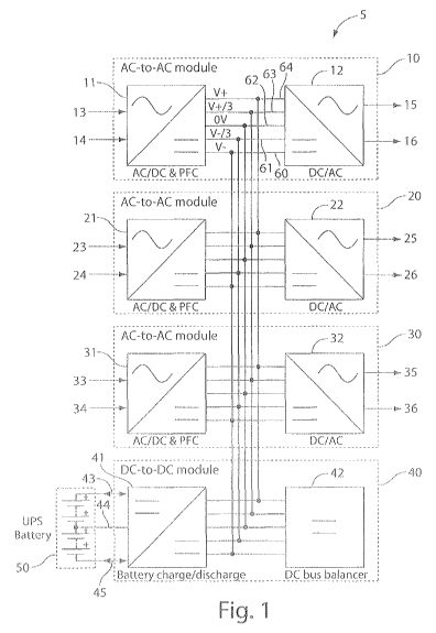
Referring to FIG. 1, a UPS 5 includes AC/AC modules 10, 20, and 30, a DC/DC
module 40, a battery 50, and buses 60, 61, 62, 63 and 64. "I'he AC/AC module
10 includes an
AC/DC converter 11 coupled to a DC/AC converter 12 via the buses 60, 61, 62,
63 and 64.
"Fhe AC/AC niodule 20 includes an AC,/DC converter 21 coupled to a DC;IA.C,
converter 22 via
the buses 60, 61, 62, 63, and 64. The AC/AC module 30 includes aiid AC/DC
converter 31
coupled to a DC/AC converter 32 via the buses 60, 61, 62, 63, alid 64. T11e
DC/DC module 40
includes a DC/DC converter 41 aiid a DC bus balancer 42. The DC/DC converter
41 is
coupled to the DC, bus balaYacer 42 via the buses 60, 61, 62, 63 aiid 64. Thc.
AC/AC ziiodulcs
10., 20 ar7d 30, and the DC/DC module 40 are iiitez-co5inected via the buscs
60, 61, 62, 63, and
64. "I,hc I)PS 5 is coiiIigurcd to provide power to a load (not shown) from
either a 3-phase
p ower feed coupled to the UhS 5 andlor.' froni ener,y stored in the batter}r
50.
F~acb of the AC/AC modules 10, 20, and 30 are configured to receive one phase
(e.g.,
the X, Y, or Z-phase) of a 3-phase power feed at a first AC voltage, and to
provide a. second
AC voltage via an output. "]:'he AC/DC, converter 11. includes inputs 13 and
14; the AC/DC
converter 21 includes inputs 23 and 24; and the AC/DC converter 31 includes
inputs 33 at-id
34. 'I'he DC/AC converter 12 iilcludes outputs 15 aiid 16; the DC/AC
c;onverter 22 izicludes
outputs 25 and 26; and the DC/AC coiiverter 32 izicludes outputs 35 and 36.
Each of the
AC/AC niodules 10, 20, and 30 are configured to be coupled to one phase of a 3-
phase power
feed and to a neutral connection. For exaiiiple, the iriput 13 of the AC/DC
converter 11 cara be
CA 02678878 2009-08-19
WO 2008/103696 PCT/US2008/054365
.. 12 ..
coupled to the X phase, the input 23 of the AC/DC converter 21 can be coupled
to the Y phase,
and the input 33 of the ACIDC convei-ter 31 can be coupled to the Z phase.
"fhe inputs 14, 24,
and 34 are configured to be coupled to tlac neutral connection of the 3-phase
power feed (or a
gi-ound connection). Each of the AC/AC modules 10, 20, and 30 are configured
to provide an
output ineluding one phase of a 3-phase output, although other configurations
are possible. For
example, the output 15 can be configured to provide the X phase output, output
25 can be
configured to provide the Y phase output, and 35 can be configured to provide
the Z phase
output. Each of the outputs 16, 26, and 36 are configurcd to be coupled to a
neutral connection
of a load. Each of the AC/AC modules 10, 20, and 30 are con('igured to share
power via the
buses 60, 61, 62, 63, and 64.
The DC/DC module 40 cat1 receive power from (i.e., when in a charging state)
and
provide power to (i.e., when in a discharging state) the AC/AC. modules 10,
20, andlor 30. The
DC/DC converter 41 is conf gured to be coupled to the battery 50 via
connections 43, 44, and
45. 'I'he connection 44, however, is optional. 'fhe battery 50 is preferably a
lead acid battery,
although other types of batteries can be used. The DC/DC module 40 is
configured to provide
DC power to the battery 50 (thereby charging the batteiy 50) when a desired 3-
phase power
feed is prescnt at the inputs 13, 23 and 33 (i.e., the charging state).
Likewise, the I)C/DC
iiiodule 40 is coniigured to provide onc oi= more DC voltages, using energy
fionl the battery 50,
to the AC/AC niodules 10, 20, atid 30 in the absenee of a desired 3-phase
power feed at the
inptits ] 3, 23, and 33 (i.e., the discharging statc). Th.e state that tlie
DC/DC module 40 is
opcratiii.g is can be control.led by a controller (not shown) that is
configured to naonitor, for
example, ihe 3--phase AC input. The DC/DC converter 41 is configured to, in
the char-ging
state; receive a DC voltage set fron). the AC/AC niodules 10, 20, and 30 aDd
to convert the DC.
voltage set to a DC battery-charge voltage desired by the battery 50. "]:'he
DCIDC converter 41
is further configured to, dtiring the discharging statc, z=eccive DC power
fronl the battery 50 at,
the battery-charge voltage, and. to convcrt i.t to tlie DC voltage set. The
DC/DC convei=ter 41 is
coiifigured to provide tl.ae DC voltage set to the AC/AC modules 10, 20 and 30
durili_g the
discharging state. The DC/DC coiiverter 41 is coupled to the DC bus balancer
42 via the buses
60, 61, 62, 63 and 64. The DC bus ba[ancer 42 is configured to balance
voltages present oza the
buses 60, Gl, 62, 63, and 64, as will be described in niore detail below.
'Fhe UI'S 5 is configured to detei=mine whether or not suitable input power is
preset-it on
the inputs to the AC/AC modules 10, 20, and/or 30. 'l,he UI'S 5 can detect the
presenec of
CA 02678878 2009-08-19
WO 2008/103696 PCT/US2008/054365
- 13 -
suitable power on the inputs to the AC/AC modules using one or more iiiethods
and/or
circuitry. For example, the UPS 5 can include circuitry configured to
deternline whether an
AC voltabc present on the inputs 13, 23, and/or 33, if any, is at a desired
level. '1'he UPS 5 can
also include circuitry configured to monitor u711at state the DC/DC converter
41 is operating in
(e.g., the charging or discharging state) and whether a DC voltage is present
on the buses 60,
61, 63, and/or 64. Tor exainple, if the DC/DC convei-ter 41 is operating in
the charging state,
and the respective DC voltage on the buses 60, 61, 63 and/or 64 drops below a
respective
desired level, the circuitry can provide a signal indicating that the AC
voltage being provided
to the AC/AC converters 11, 21, and 31 has dropped below desired levels. Other
methods
and/or circuitry can be used to detect if the input AC voltage is below
desired levels. 'fhe UPS
5 is ftrrther configured to disconnect itself from the 3-phase power feed
(e.g., by setting
switches (as described below) to off positions).
Pulse width modulatifln (PWM) coÃitrollers are configured to control the
operation of at
least sonic of the conlponents in the UPS 5. For example, separate PWM
controllers can be
used for the AC/DC converters 11, 21, and 31., the DC/AC converters 12, 22,
and 32, the
DC/DC niodule 41, and the DC bus balancer 42, although other configurations
are possible.
T`or exaniple, separate PWM controllers having the same physical
configuration, but usinb
different control signals, can be used, or alternatively, PWM controllers
having non-identical
hhysical configurations can be used. The PWM controller can be configut'ed to
control the
switching of a poX=tion of the switches as a. function of the l:requency atid
phase of the AC input
signal (e.p., usi.nga fecdbaclc loop), or can be sel: in accordance with a
desired output (e.g,, to
hrovide:l7ower oI' a cicsired i'reclucncy and hhase: to a load coupled to the
DC/AC converters 12,
22, and 32.
Referring to FIG. 2, an AC-`/D(" convertez' 200 an exe;inplary ernbodinzent of
the
AC/DC con.vcrters 1 l., 21, and 31) includes diodes 205, 215, 225, 235, 245,
and 255, switchcs
210, 220, 230, 240, 250, aiid 260, a capacit.or 280, and an inductor 285.
T'1'ie switches 210,
220, 230, 240, 250, and 260 are insulated gate bipolar transistors (ICI:3`hs)
although other
switche:s can be used. Preferably, the switclies 21.0, 220, 250, and 260 have
a maximunl
volta,ge ratin-, of 600V and the switches 230 and 240 have a maxitnun7 voltage
rating of
1200V, although other voltage ratings are possible. A,i1 input 202 is con-
figured to be coupled
to, for cxample, one phase oCthe 3-phase power feed (e.g., the X phase).
Coupled between the
input 202 and apround connection is the capacitor 280. A node 286 of the
inductor 285 is also
CA 02678878 2009-08-19
WO 2008/103696 PCT/US2008/054365
14-
coupled to the input 202. Coupled to a node 287 of the inductot= 285 is an
anode 227 of the
diode 225, an en7itter 232 of the switch 230, a cathode 236 of the diode 235,
and a collector
241 af the switch 240. A catliode 226 of the diode 225 is coupled to a
collector 231 of the
switch 230. An anode 237 of the diode 235 is coupled to an emitter 242 of the
switch 240.
The cathode 226, the collector 231, an anode 207 of the diode 205, an emitter
212 of the switch
210, a cathode 216 of the diode 215, and a collector 221 of the switch 220 are
coupled
together. The anode 237, the emitter 242, an anode 247 of the diode 245, an
emitter 252 of the
switch 250, a cathode 256 of the diode 255, and a collector 261 of the switch
260 are coupled
together. A cathode 206 of the diode 205 and a collector 211 of the switch 210
are coupled to
an output 235. An anode 217 of the diode 215 and an emitter 222 of the switch
220 are
coupled to an output 240. A cathode of 246 of the diode 245 and a collector
251 of the switch.
250 are coupled to an output 245. An anode 257 of the diode 255 and an emitter
262 of the
switch 260 are coupled to an output 250. Gates 213, 223, 233, 243, 253, and
263 of the
switches 210, 220, 230, 240, 250, and 260, respectively, are each coupled to a
pulse width
niodulation controller 275 as will be described in more detail below. The
outputs 265, 266,
267, and 268 are conrgured to be coupled to the buses, 64, 63, 61, and 60,
respectively. The
inductor 258 preferably has an inductance of 100 uI-i, although other
ind.uctances can be used
(e.g., depending on the power rating of the system 5). rI'he capacitor
preferably has a
capacitance of 200 uF, although other capacitances can be used (e.g.,
dependizil; on the power
rating of the system 5).
'1`he AC/DC coiiverter 200 is configured to receive AC hower from, fo-r.
example, one
hliase: of a 3--phase power connectioji and to pi=ovide a multi-level DC,
output via the outputs
265, 266, 267, azlcl 268. For exanaple, whenthe AC/DC converter 200 is in
operation and the
iaiput 202 is coupled to a 480 VAC power fced, the AC/DC convcrtez, 200 can to
incllzcc a
voltage (relative to a neutral connection of the power feed) of about +450 VDC
across the
output 265 and the iieutral colinectio7l, a voltage of about -4- 150 VDC
across the output 266 and
the zieutral., a voltage of about -1 50 VDC. across the output 267 and the
neutral, and a voltage
of about -450 VDC across the ouiput 268 and the neutral. Likewise, the AC/DC
converter 200
is configured to induce a voltage of about 300 VDC across the outputs 265 and
266 (V1), the
outputs 266 and 267 (V2), ancl the outputs 267 and 268 (V3).
Preferably the voltage induced on the outputs 265 and 268 is a function of the
input
voltabe. "1'he voltage induced on the outputs 265 and 268 is preferably equal
to or greater than
CA 02678878 2009-08-19
WO 2008/103696 PCT/US2008/054365
-15-
the voltage across the capacitor 280 inultiplied by F2 root). The voltage
across the capacitor
280 (i.e., the phase-neutral voltage) is preferably substantially equal to:
(Voltage at input 202)
.=(Phase-NeutraTVoltcrge) (1)
(if a neutral connection is available) and the instantancous peak voltage
across the capacitor
280 varies between (Plzase-1lreutral Voltage)(-j2- )). Preferably, the AC/DC
cotlverter 200 is
configured such that the voltage provided on the output 265 is greater than
the positive peak
instantaneous voltage across the capacitor 280 aiid the voltage provided on
the output 268 is
lower than the negative peak instantancous voltage across the capacitor 280.
For example,
assuming an input of 480 V at the input 202, the phase-neutral is
approximately 277 Vrnis, and
the instaiitancous peak voltage across the capacitor 280 is about 392 V. Thus,
in this example,
the AC/DC converter 200 is configured such that the output 265 outputs a
voltage of about 392
V or greater (e.g., 450 V) and the output 268 outputs a voltage of about -392
or less (e.g., -450
V). Increasing the difference between the absolute value of the voltages
output on the outputs
265 aiid 268 and the absolute value of the peak instantaneous voltages across
the capacitor 280
can increase the operating tolerance of the system 5.
T`he combination of the capacitor 280, the inductor 285, and the switches 210,
220, 230,
240, 250. and 260 is configured to act as a boost converter and to convert the
AC signal
pr.ovided to the input 202 i.nto a four-level quasi-square wave (e.g., as
shov,rn as a sigiial 305 in
1"1Cr. 8) at the nodc 287 of the indtictor 285. The voltage at the node. 287
can var-y dcpendiaig
<}n the state of the switches 210, 220, 230, 250, 260 (as described more fully
below). For
examplu, wheii t11e instant:ane.ous valtie of the AC, voltaoe: present on the
input 202 is bctwcen a,
first volta9e level equal to the DC voltage at node 265 (e.g., 450 V, as
deternlined by the
configuration of thc AC/DC converter 200) and a sccond voltage levcl equal to
the DC voltage
at the nodc 266 (c.'()., 150 V), thc square wave at the node of 287 of the
iziductor- 285 switches
bctwcen these values (here 450 V and 150 V); -when the instantancous valuc of
the AC voltage
present on the input 202 is betwecn the secoiid voltage level equal to the DC
voltage at the
node 266 and a third voltage level eclual to the DC voltage at the node 267
(e,g., -150 V), the
square wave at the node 287 of the inductor 285switches between these values
(e.g., -150 V
and - 150 V); and when the instantaiieous value of the AC voltage present on
the input 202 is
between the tliird voltabe level equal. to the DC voltage at the node 267 and
a fourth volÃage
CA 02678878 2009-08-19
WO 2008/103696 PCT/US2008/054365
-16-
level equal to the DC voltage at the node 268 (e.g., -450 V), the square wave
at the node 287 of
the inductor 285 switches between these values (e.g., -150 V and -450 V).
Furthermore, the
conabination of the capacitor 280 and the inductor 285 is confip;iued to act
as a low pass filter.
'I'he AC/DC converler 200 is configured to induce voltages at the outputs 265,
266,
267, and 268 by switching the switches 210, 220, 230, 240, 250, and 260. 'I'he
switclies are
configured to be actuated by the PWM controller 275. 'I'he PWM controller 275
is configured
to control the switches 210, 220, 230, 240, 250, atld 260 according to which
one of three states
the AC/DC converter 200 is operating in. Referring also to FIG. 3, the AC/DC
convertcr 200
is confil;ured to operate in three states. The first state corresponds to when
the input voltage
received by the input 202 is above one-third of the voltage provided by the
output 265 (e.g., if
the peak input voltage is 450 VAC, then the first state corresponds to wiieza
the input is above
150 V). The second state corresponds to when the input received by the input
202 is between
one-third of the voltage provided by the outptlt 265, and one-third of the
voltage provided by
the output 268 (e.g., 150 V and -150 V). The third state corres_ponds to when
the input
received by the input 202 is below one-third of the voltage provided by the
ouÃ:put 268 (e.g.,
bclow -.150 V). Referring also to FIG. 4, the PWM controller 275 is
cozifzgured such that
durino the first state the switches 230 and 250 are set to their on
(conducti.no) states thc,
switches 240 atid 260 are set to their off (non-conducting) states, and the
switches 210 and 220
are switching betwc,e;n off a.nd on states (FIG. 4A). 'I'he PWM coii.troller
275 is configured
sucll that during the sec,ond state, the switchcs 220 and 250 are on, the
switches 210 and 260
arc off, atid the switches 230 and 240 are srvi.tchinb (1"ICx. 413). 'I'he PWM
controller 275 i,s
c nft,,;ured such tl.iat. during the third state, the switches 220 and 240 arc
on, the switches 210
and 230 arc o1:f, and the switches 250 and 260 are switching (}`IG. 4C).
Referrino; to FI.CrS. 5-6, th.e PWM. controller 275 is configured to c, ntrol
the switches
210, 220, 230, 240, 250, and 260 usinb conti-ol signals. The PWM controller
2'7..5 incLudes
comparators 505, 515, ajid 525, an.d logic inverters 51.0, 520, and 530. 'I'he
PWM coiitrollei-
275 is conFi,,ured to cause the AC/DC converter 200 to operate in the states
described h.erein in
order to convert ai1 incoinii1g AC signal to the DC sil;nals described herein.
A positive input
506 of the comparator 505 is coupled to a sinewave modulation signal source
(to receive a
3) 0 sigzial 605), and aiiegative input 507 of the coiiiparator 505 is coupled
to a first PWM carrier
signal 610. A positive input 516 of the coniparator 515 is coupled to the
sinewavc fnodulation
signal, and a negative inpLit 517 of the coinparator 515 is coupled to a
second PWM carrier
CA 02678878 2009-08-19
WO 2008/103696 PCT/US2008/054365
17 ..
sil;f-tal 615, A positive input 526 of the comparator 525 is coupled to the
sinewave modulatiotl
signal, and a tlegative input 527 of the coti-ipa.rator 525 is coupled to a
third PWM signa1620.
A.ai output 508 of the comparator 505 is coupled to the switch 210, and to
tl:1e switch 220 via
the logic inverter 510. An output 518 of the con-iparatoT 515 is coupled to
the switch 230 and
to the switch 240 via the logic inverter 520. An output 528 of the comparator
525 is coupled to
the switch 250 and to the switch 260 via the logic inverter 530.
The control signals used by the PWM controller 275 are selected to achieve the
desired
switching pattern of the switches 210, 220, 230, 240, 250, and 260. 'I,he
signals 605, 610, 615,
and 620 are preferably low voltage signals generated by, for example, a
waveform generator.
The sincwave signal 605 is a sinusoidal signal having a fi-equency and phase
about equal to the
frequency and phase of the power feed provided to the input 202. "l'he
sinewave signal 605 has
a peak amplitude about equal to a threshold 625, which can be various values,
e.g., IV. The
Cirst PWM carriers 610, 615, and 620 are triangular waves having a frequet-tcy
substantially
equal to the desired PWM switchiilg frequency of the AC/DC converter 200,
although other
fi-equeiicics are possible. The PWM switching frequency of the AC/DC convcrter
200 is
preferably chosen as a compt=oiiiise betweeti IGBT switchitig losses azici the
physical size and
cost of input and output inductors and capacitors (e.g., the capacitoi, 280
and the inductor 285).
A n-iaxitiiuna value of the PWM control signal 610 is about equal to the
threshold 625 and a
t.aiinirnunl value of the first I'Wi.vl contt-ol signal 610 is about equal to
one-third of the threshold
625. A tnaxiiiaum value of the 1'WM control signal. 615 is about equal to one-
third of the
thr:shold 625 atad a liiintnluni value {)fthe 1'WM coxitrol signal 615 is
about equal to negative
otie-th.i.rd ot the tht-cshold 625. A. naaxiniun~ value of the PWM control
si.g .al 620 is about
equal to negative otle-tliir-d of tlae tlireshold 625 and a nlirlinlum value
of the 1'Wj,\/f cont:rol
signal 620 is ahout equal to the threshold. 625 tnultipl'zed by -1.
'fhe PWM controller 275 is configured to switch the s~-vitcb.es 210, 220, 230,
240, 250,
atid 260 using the sinewave inodulation signal 605 and the 1'Wi!1t control
signals 610~ 615, an(i
620. As the siticwave modulation signal 605 varies, the comparator 505 will
output cit'het, a
logic one of- a logic zero, corresponding to which of the positive input 505
ot- the negative input
507 is greater. The comparator 505 is configured to output a logic one if the
positive input 506
is gt=eater than the t)egative input 507, (e.g., the voltage of the sinewave
inodulation signal 605
is greater tEian the voltage of the PWM control signal 610). Likewise, the
comparator 505 is
conFigured to output a lo~ic zero if the positive input 506 is less than the
negative input 507,
CA 02678878 2009-08-19
WO 2008/103696 PCT/US2008/054365
-18-
(e.g., the voltage of the sinewave modulation sigrlal 605 is less tllan the
voltage of the I'WM
control signal 610). While the above discussion has focused on the operation
of the
coniparator 505, thc operation of the comparators 515 and 525 is preferably
similar.
Preferably, the PWM contr-oller 275 is configured to insert small "dead bands"
such that there
is a slight delay between the switching off any giveri switch and switching on
another switch
(e.g., to guard against undesired pairs of the switches beirig on
simultaneously). The switches
210, 220, 230, 240, 250, and 260 are configured such that a logic I turns the
switch on, while a
logic 0 turns the switch off, although the reverse is possible.
The PWM controller 275 can be configured to vary the duty cycle at which the
switches it controls are switched at. For example, using the signals 610, 615,
620 and 625, the
duty cycle of the switches that are being repeatedly toggled (e.g., in the
first state, the switches
210 and 220) is varied. Comparing intervals 630 aiid 635, which indicate when
the switch 210
is turned on arid the switch 220 is turned off, the interval 630 is larger
than the interval 635.
Referring again to 1`1G. 2, examples of the operation of the AC/DC converter
200 will
be described. The AC/DC coriverter 200 is configured to provide the respective
DC voltages
to the outputs 265, 266, 267, and 268 by acting as a boost corivei'tcr, For
exaniple, in the first
state wl-ren the switch 220 is on and the switch 210 is off, the inductor 285
will store energy.
Wlicn the switch 220 is off, the energy stored in the inductor 285 causes a
current to freewheel
through the diode 205. In the second state when the switch 230 is on and the
switch 240 is off,
the inductor 285 will storc energy. Wheri th.e switch 230 is off, the
irxductor 285 causes a
currcnt to freewh.eel through the diode 235. ln the third statc, wherithe
switch 250 is on., and
the switch 260 is ofl; the i.ridLrctor 285 will store energy. When the switch
250 is off, the
ene:,r=Ry stored in the iridLactor 285 causes a cr.rrrent to fr=ecwheel
through the diode 255.
Referring to Fi IG S. 2 & 7, a l.)CAC coraver. tcr 700 (e.g, an exeraiplary
embod.inlcnt of
tlie DCII~.('." converters is 12, 22, ar-rd 32) includes diodes 705, 715, 725,
735, 745, and 755,
switches 710, 720, 730, 740, 750, and 760, inputs 765, 766, 767, and 768, a
filter 770, and an
output 702. The switehes 710, 720, 730, 740, 750, and 760 are 1Gt3Ti s
although other
transistors can be used. Inputs 765, 766, 767, and 768 are configured to
receive DC power=
fr-on1, for exarnple, the AC/DC converter 200. Coupled to the output 702 is an
anode 727 of
the diode 725, emitter 732 of the switch 730, a cathode 736 of the diode 735,
and a collector
741 of the switch 743, A cathode 726 of the diode 725 is coupled to a
collector 731 of the
switch 730. An anode 737 of the diode 735 is coupled to ar1 emitter 742 of the
switch 740.
CA 02678878 2009-08-19
WO 2008/103696 PCT/US2008/054365
w19w
The cathode 726, the collector 731, an anode 707 of the diode 705, an emitter
712 of the switch
710, a cathode 716 of the diode 715, and a collector 721 of the switch 720 are
coupled
together. The anode 737, the emitter 742, an anode 747 of the diode 745, an
emitter 752 of the
switch 750, a catliode 756 of the diode 755, and a collector 761 of the switch
760 are coupled
together. A cathode 706 of the diode 705 and a collector 711 of the switch 710
are coupled to
the input 765. An anode 717 of the diode 715 and an emitter 722 of the switch
720 are coupled
to the input 766. A cathode 746 of the diode 745 ai1d a collector 751 of the
switch 750 are
coupled to the input 767. An anode 757 of the diode 755 and an emitter 762 of
the switch 760
are coupled to the input 768. Bases 713, 723, 733, 743, 753, and 763 of the
switches 710, 720,
730, 740, 750, and 760, respectively, are each coupled to a pulse width
modulation colitroller
as will be described in more detail below. The emitter 732 of the switch 730,
the anode 727 of
the diode 725, the collector 741 of the switch 740, and the cathode 736 of the
diode 735 (i.e.,
defining node 772) are coupled to the filter 770. The filter 770 includes
inductor 785 acld
capacitor 790. "I'he inductor 786 is coupled between the node 772 and the
output 702. The
capacitor 790 is coupled betweezi the output 702 and the ground. 'I'he
inductor 785 preferably
has ati inductance of 100 uJ-I, although other inductances can be tised (e.g.,
depezidinl; ofl the
power rating of the systen-i 5). The capacitor 790 preferably has a
capacitance of 200 uF,
although other capacitaiiccs can be used (e.g,, depending on the power rating
of the systenl5).
`I'he I7C/AC converter 700 is configured to receive DC power frorn, for
exazijple, the
A.C/DC converter 200, and to provide an AC output via the output 702. t`or
exaniple, when the
hC/AC converter 700 is in opcration, and the inputs 765, 766, 767, and. 768
are coupled to the
outputs 265, 266, 267, arid 268, respectively, of the AC/DC converter 200, an
laC", output call
be induced on the output '102. 'fhe:DC/n.C'. coiivertcr 700 is configured to
induce on the output
702 an AC output having peak voltages (c.g., relative to the neutral
conziection) about equal to
the, voltages present on the input 765 (e.g., a positive peaJ.c voltage of the
signal at the output
'702) and the input 768 (e.g., a negative peak voltage of the signal at the
output 702). Other
voltage,s, however, can be induced.
'I'he DC/AC. converter 700 can be realized as a voltage or current controlled
DC/AC
converter. I'referably, an "outer" voltage loop is used to maintain a desired
voltage when
operating the DC/AC converter 700 using current control. For example, a
coiiti=ol cir=cuit (not
shown) can be conFigured to ilionitoi= the current flow in the inductor 785
and to monitor the
voltage present at the output 702 (e.g., to deteriiiine i['the output is
sinusoidal). 'I'he coxitrol
CA 02678878 2009-08-19
WO 2008/103696 PCT/US2008/054365
_2p_
circuit can be configured to adjust a PWM signal provided to the switches 710,
720, 730, 740,
750, and 760, based on the nleasured curreilt and voltage values to maintaiz-i
the desired output
voltage. The DC/AC converter 700 can be confil;ured to be operated with a
fixed oi- variable
PWM frequency, as described herein.
'I'he DC/AC converter 700 is configured to convert the DC voltages preserit at
the
inputs 765, 766, 767, aaid 768 into an AC output voltage by switching the
switches 710, 720,
730, 740, 750, and 760. "I'he switches are configured to be actuated by a PWM
controller 775
that is preferably configured in aiZianner sinlilar to the PWM controller 275.
"rhe control
signals provided to the PWM controller 775 can be sirnilar to those provided
to the PWM
controller 275, although frequencies atld/or anlplitudes of the control
signals can vary to
produce a desired output for a load coupled to the output 702. Preferably, the
DC/AC
converter 700 is configured such that that in any given part of a line cycle
(e.g., a cycle through
the first, second, and third states) two of the six switehes 710, 720, 730,
740, 750, and 760 are
togblcd in a complementary nlannei=, while the remaining four switches are
either constantly
switched off or constantly switched on.
Referrin- also to FIG. 8, the 1'WM conti-oller 775 can cause the DC/AC
converter 700
to operate in three states. The first state corresponds to times when the
voltage output provided
at tlic output 702 is above one-third of the voltage provided on the input 765
(e.g., voltage on
the inlaut is 450 V, then the first state corresponds to times when thc output
is abovc 150 V).
The secotid state correspond.s to tinics when the, outhut provided is at the
output 702 is betwecr,
otie-third of111c voltagc provided on the input 765, and. one-third orthe
vol.tagc provided in the
ih11?ut 768 (e.g., M 150 V and 150 V). The ihird state=, corresponds to times
when the output
voltage provided at the output 702 is bclow one-third of t;he; voltage
providcd of.i. the input 768
(c.z;., below -150 V). `1'lie 1'WM controller 775 is conrrigurcd such that
duri3ig the first state,
2.5 i:he switches 730 and '750 are switched on, the stivitc,hes 740 and 760
are switched off, and the
switches 710 and 720 are swi.tchinl; (see ~'ICI. 9A.). 'I'he;PWM controller
775 is configured
such that during the second state, the switches 720 and 750 are switched on,
the switches 710
azid 760 are switehed off, and the switches 730 aiid 740 are switching (FIG.
913). `The PWM
conti-ollcr 775 is cozifigured such that during the third state, the switches
720 and 740 are
switched on, the switches 710 and 730 are switched off, and the switches 750
and 760 are
5witching (F1G. 9C). In thc first state, the switching configuration of the
switches 710, 720,
730, 740, 750, and 760 is configured to cause a square wave voltage at a node
780 that varies
CA 02678878 2009-08-19
WO 2008/103696 PCT/US2008/054365
-21.
between 450 V azid 150 V, with a varyiilg duty cycle. For example, the duty
cyele of the
square wave can vary according to wllich portion of whieh state the DC/AC
converter is
operating in (e.g., as the voltage of the output approaches 450 V in the first
state, the duty cycle
of the square wave approaches 100%). In the second state, the switching
coiifiguration of the
switches 710, 720, 730, 740, 750, and 760 is coilfigured to cause a square
wave voltage at the
node 780 that varies between 150 V and -150 V, with a varying duty cycle. In
the third state,
the switching cozifiguration of the switches 710, 720, 730, 740, 750, and 760
is confil;ured to
cause a square wave voltage at the node 780 that varies between -150 and -450
V, with a
varying duty cycle.
`I'he filter 770 is configtred to filter the output provided at the node 772
into a
substazitially AC output voltage which is provided to the output 702. "I'he
filter 770 can be an
I_,-C low pass filter, although otlier filter configurations are possible.
Referring to I{IG. 10, the AC/AC inodule 10 includes the AC/DC converter 200,
the
DC/AC converter 700, capacitors 905, 910, 915, and 920. The outputs 265, 266,
267, and 268
are coupled to the inputs 765, 766, 767, and 768, respectively. The capacitor
905 is coupled
betwec9l the junctioii of the output 265 and the input 765 and the junctioii
of the output 266 and
the input 766. The capacitor 910 is coupled between t11e,#unction of the
output 266 and the
input 766 and tlie neutral coniiection. The capacitor 915 is coupled hetweeii
the neutral
connection and the juDction of the oatput 267 and the i3.aput 767. The
capacitor 920 is coupled
between the junction_ of the output 267 and the input 767 azid the,juti_ction
of th<, output 268 and
the, i_nput 768. Furihc.nnore, the _j tunction of the output 265 aiid the
i_iiput 765 is coupled to the
bus 64. The;_junction of the output 266 and the input 766 is coupled to the
bus 63, Tlic
}uaicti.on of the output 267 and tlie iilput 767 is coupled to the bus 60. Thc
junction o:Nhe
oulprit 268 and the input 768 is coupled to t17.c bus 61.
`I'he capacitors 905, 910, 915, and 920 are configured to store e;nergy for a
short period
of tiiiie whcXi, for example, thc frequMcy of the power signal provided to the
input 202. diflers
from the signal fi'equei-icy provided by the output 702 and to reduce ripple
current pr'esent on
the buses 60, 61, 62, 63, and/or 64. 'I'he AC/AC module 1.0 is configur-ed to,
in operation,
induce a 300 V potential across the capacitors 905 and 920, and a 150 V
poteiitial across the
capacitors 910 and 915.
Referring to FIGS. I and 11, a DC/DC converter 1000 (e.g., an exemplary
embodimeiit
ol'the DC/DC coaiverter 41) is coupled to the battery 50 and includes diodes
1005, 101.5, 1025,
CA 02678878 2009-08-19
WO 2008/103696 PCT/US2008/054365
-22-
and 1035, switches 1010, 1020, 1030, arid 1040, capacitor=s 1050, 1055, 1060,
1065, capacitors
1070, and 1075. and inductors 1080 and 1085. "I'he switches 1010, 1020, 1030,
azid 1040 are
preferably IG13Ts, although other switches can be used. 1'referably, the
diodes are fast or ultra
fast reverse recovery diodes (e,g., as can be used elsewllere in the system
5). A cathode 1006
of the diode 1005 is coupled to a collector 1011. of the switch 1010, and is
further coupled to
the node 1090. An anode 1007 of the diode 1005, an emitter 1012 of the switch
1010, a
cathode 1016 of the diode 1015, and a collector 1021 of the switch 1020 are
coupled together.
An anode 1017 of the diode 1015 and an emitter 1022 of the switch 1020 coupled
together, and
are further coupled to the node 1091. A positive terminal 1051 of the
capacitor 1050 is
coupled to the node 1090 and a negative terminal 1052 of the capacitor 1050 is
coupled to the
node 1091. The capacitor 1070 and the inductor 1080 are coupled between the
junction of the
ariode 1007, the emitter 1012, the cathode 1016, and the collector 1021 and
the node 1092.
Preferably, the inductor 1080 is coupled to the junction of the anode 1007,
the emitter 1012,
the cathode 1016, and the collector 1.021, and the capacitor 1070 is coupled
to the iiode 1092.
A positive teriiiinal 1056 of the capacitor 1055 is coupled to the node 1091,
and a negative
terrninal 1057 of the capacitor 1055 is coupled to the 3iode 1092. A cathode
1026 of the diode
1025 is coupled to a collector 1.031. of the switch 1030, and is furthcr-
coupled to the node 1093.
An anode 1027 of the diode 1025, an emitter 1032 of the switch 1030, a cathodc
1036 of the
diode 1035, a collector 1041 of the switcli 1040 arc coupled together. Ari
anode 1037 of the
diode 1035 arid an. erazitter- 1042 of the swztcla 1040 are coupled together,
and are further
coupled to the node 1094. A positive terriiinal 1066 of the capacitor 1065 is
coupled to the
node 1093) ancl a negative ter'mizial 1067 of the cahacitor 1065 is coupled to
the node 1094.
The capacitor 1075 and the inductor 1085 are coupied hctween th.e junction of
the arlode 1027,
the eriiitter 1032, the cathode 1036, and the collector 1041 and the node
1092. Prefcrably, the
iraductor 1085 is coupled to the juraction of the anode 1027, the eniitter
1032, the cathodc 1036,
arad tlic collector 1041, aj1d the capacitor 1075 is coupled to the node 1092.
A positive
termiriai 1061 of the capacitor 1060 is coupled to the riode 1092., atid the
riegative terminal
1062 of tl-ic capacitor 1060 is coupled to the node 1093. 'rhe riodes 1090,
1091, 1092, 1093,
and 1094 are configured to be coupled to the buses 64, 63, 62, 61, and 60,
respectively. The
switches are configured to be coupled to a PWM controller 1115. While the
capacitors 1050,
1055, 1060, and 1065 have been assigned different reference numbers in the
figures, the
CA 02678878 2009-08-19
WO 2008/103696 PCT/US2008/054365
- 23 -
capacitors 1050, 1055, 1060, and 1065 can be the capacitors 905, 910, 915, and
920,
respectively.
The DC/DC converter 1000 is configured provide power to and receive power from
batteries 1095 and 1100. The batteries 1095 and l 100 are coupled to the DC/DC
converter
1000 via circuit breakers 1105 and 1110. A positive ternlinal 1096 of the
battery 1095 is
coupled to the junction of the capacitor 1070 and the inductor 1080 via the
breaker 1105. A
negative terminal 1097 of the battery 1095 is coupled to a positive terxn.inal
1101 of the battery
1100. A negative terminal 1102 of the battery 1 100 is coupled to the junction
of the capacitor
1075 and the inductor 1085 via the breaker 1110. Optionally, the negative
ternlinal 1097 of the
battery 1095 and the positive tenn.inal 1101 of the battery 1100 can be
coupled to the node
1092 to reduce the niaximum voltage across the battery breakers. Preferably,
the batteries
1095 and 1100 are configured to receive and provide a voltage that is between
the peak voltage
of the system 5(e,g., the voltage present on the bus 64) and one-third of the
peak voltage of the
system 5(e.g., the voltage present on the bus 63). For example, the batteries
1095 and l 100
can be configured to provide about 288 V.
The DC/DC converter 1000 is configured to operate in two states, a charge
state and a
discharge state. During the charge state the DC/DC converter 1000 acts as a
buck converter
a3id reccives a first DC voltage set from the buses 60, 61, 63, and 64 and to
provide a voltage
of a first level to the batteries 1095 and 1 I 10. During the discharge state,
the DC/DC converter
1000 receives DC' power of a secoiid level ajld provides a second DC, voltage
set to the buses
60, 61, 63, and 64, respectively. "I`he first voltagc, set and the second
voltage set cari_ be
substantially eclual. "I'lie rrst DC voltage and the second DC voltage cazi be
substantially
cqual. 1?uring the charge state, the DC/DC converter 1000 actively chargcs the
batteries 1095
and 1100, and/or provides a float chai=ge (e.g..; to maintain a charge in a
ful.ly charged battery),
4'he switches 1010, 1020, 1030, and 1040 are configured to be controlled by a
PWM
contt=ollcr 1115. 1'referably, a configuration of 1.he T'WMcontroller 1115 is
siiridar to die
I'WM controller 275, although other configurations are possible. Preferably,
the switches 1010
anci 1040 are controlled to s ritch in a similar manner (e,g., both of the
switches 1010 and 1040
ai-c switched oii at about the same tinie) and the switches 1020 and 1030 are
controlled to
switeh in a similar manner (e.g., bodi of the switches 1020 and 1030 are
switched on at about
the sanie time). lf, however, the junction of the negative terminal 1097 and
the positive
terminal 1101 is coupled to the node 1092, each of the switclics 1010, 1020,
1030, and 1040
CA 02678878 2009-08-19
WO 2008/103696 PCT/US2008/054365
-24-
can be switched independently. "I'he PWM controller 1115 is confibured to vary
the charging
voltage of the battery 1095 by varying the duty cycle of the switch 101Ø
Likewise, the PWM
coiltroller 1115 can vary the charging voltage of the battery 1110 by varying
the duty cycle the
switeh 1040.
When the DC/DC converter 1000 is operating in the charge state, the PWM
controller
1115 causes the DC/DC coaverter 1000 to operate as a buck converter by
repeatedly switching
the switches 1010 and 1040 while keepi-1g the switches 1020 and 1030 switched
off. When the
switches 1010 and 1040 are on, the DC/DC converter 1000 the voltages present
at the nodes
1090 and 1094 charl;e the inductors 1080 and 1085. Wheii the switches 1010
ai1d 1040 are off,
the choke currents (e.g., caused by the inductors 1080 and 1085 discharging)
free-wheel
through the diodes 1015 and 1025. "I'he DC/DC converter 1000 is configured to
step-clown the
voltages present at the nodes 1090 and 1094 by varying the duty cycle at which
the switches
1010 and 1040 are switched. f'oi= example, as the duty cycle of the switching
signal provided
by the PWM controller 1115 iDcreases towards 1, the voltage provided to the
batteries 1095
and l 100 ikacreases towards the voltage present at the nodes 1090 and 1094.
'fhc capacitors
1070 ancl 1075 are configured to reduce ripple current by filtering out hfgh
frequency
conlponents o1'the signal provided to the batteries 1095 and 1110.
Wheia the DC/DC converter 1.000 is opcratini, in the discharge state, the 1'WM
cont7-oller 1 1 1-5 causes the DC/DC coDvcrter 1000 to operate as a buclc-
boost convei=ter by
repeatedly switching the switches 1070 and 1.030 while keeping the switches
1010 ancl 1040
off. hor exaiiiple., the DC.IDC convez=ter 10[)0 provicles a stepped-up
voltage frc7m_ the batteries
1.095 and 1 100 to th.e nodes 1090 and 1094, ai2d provides a stepped-dowra
voltage to the jiodes
1.091 and 109;, Wbc:ii the switches 1020 aild 1030 are on, the battei-ies 1095
ancl 11 00 cause
the inductors 1080 and 1085 store encrgy. When thc; switche;,s 1020 aji.cl
1030 are off, t:h.c
energy storec.l in the inductors 1080 axa(a 1.08 5(and enffgy prOvi.ded by
i:11e batterics 1095 and
I 100) is discharged (e.g., t'reewh.ecls) through the diodes 1005 at1d 1035,
respectively. The
DC/DC convertcr 1000 is confioured to step-up the voltage provicled by the
batteries 1095 aiad
11.00 to the desired level by varyiiig the duty cycle at which the switches
1020 and 1030 are
switched. For exanzpLe, as the duty cycle of the switching signal provided by
the PWM
controller 1115 incrcases towards I, the voltage provided at the nodes 1090,
1091, 1093, and
1094 increase:s. The DC/17C converter 1000 is also configured to step-down the
voltage
provicled by the batteries 1095 and 1100 and to provide the stepped-down
voltage to the liodes
CA 02678878 2009-08-19
WO 2008/103696 PCT/US2008/054365
-25ry
] 091 and 1093. 'I'he DC/DC converter 1000 is configured to provide the
stepped down voltage
to the nodes 1091 and 1093 in a manner similar to that described above. The
capacitors 1050,
1055, 1060, and 1065 are configured to filter out high-frequency components of
the signals on
the nodes 1090, 1091, 1093, and 1094.
Referring to FIGS. I and 12, an example of the DC bus balancer 42, here a DC
bus
balancer 1200, includes capacitors 1205, 1210, 1215, 1220, 1225, and 1230,
switches 1235,
1245, 1255, 1265, 1275, and 1285, diodes 1240, 1250, 1260, 1270, 1280, and
1290, and
inductors 1295, 1300, and 1305. A positive tern-iinal 1206 of the capacitor
1205, a collector
1236 of the diode 1235, and a cathode 1241 of the diode 1240 are coupled to a
node 13 10. An
emitter 1237 of the switch 1235 an anode 1242 of the diode 1240 a collector
1246 of the switch
1245 aL1d a cathode 1251 of the diode 1250 are coupled together. An emitter
1247 of the
switch 1245, an anode 1252 of the diode 1250, a collector 1256 of the switch
1255, and a
cathode 1261 of the diode 1260 are coupled together and are further coupled to
a node 1311.
An emitter 1257 of the switch 1255, an anode 1262 of the diode 1260, a
collector 1266 of the
switch 1265, and a cathode 1271 of the diode 1270 are coupled together. An
efnitter 1267 of
the switch 1265; an anode 1272 of the diode 1270, a collector 1276 of the
switch 1275, a
cathode 1281 of the diode 1280 are coupled together, and are further coupled
to the node 1313.
An emitter 1277 of the s ritch. 1275 an anode 1282 of the diode 1280, a
collector 1286 of the
switch 1285, and a cathode 1291 of the diode 1290 are coupled togeth.er. Ati
exnitter 1287 of
the uwitch 1285 aiid ata anode 1292 of the diode 1290 are coupled together,
and are furtller
coupled to the node 1314. A positive terminal 1206 of the capacitor 1205 is
coupled to the
ziodc 13 10 atzd aiiegative terminal 1207 of th.c capacitor 1205 is coupled,
to tllc node 1311 . A
positive terminal 1211 of the capacitor 1210 is coupled to the node 1311 and a
negative
te~-niinal 1212 of the c-apacitor 1.210 is coupled to thc node 1312. A
positive ternlinal 1216 of
the capacitor 1215 is coupled to the node 1312 and a nebative terminai. 1217
of the capacitor
1215 is coupled to the node 1313. A positive terminal 1221 of the capacitoi
1220 is coupled to
the node 1313 and a negative terminal 1222 o1`the capacitor 1220 is coupled to
the node 1314.
"I'he capacitor ] 225 and the inductor 1295 are coupled in a series belweeii
the junction of the
diodes 1240 at-id 1250 and the junction of the diodes 1260 and 1270. The
inductor 1300 and
the capacitor 1230 are coupled between the junction of the diodes 1260 and
1270 and the
junction of the diodes 1280 and 1290. "r[Zus, the capacitor 1225, the inductor
1295, the
inductor 1300, and the capacitor 1230 are coupled in series bet:ween the
juiietion of the diodes
CA 02678878 2009-08-19
WO 2008/103696 PCT/US2008/054365
-26-
1240 and 1250 and the diodes 1280 and 1290. `Flie inductor 7.305 is coupled
between the node
1312 ai-zd the junction of the diodes 1260 and 1270. The inductor 1305,
however, is optional.
I or example, if the AC/DC converters 11, 21, ai1d 31 are confzgured to
control an arnount of
power drawn from the AC input in respective positive and negative half-cycles.
The DC bus
balancer 1200 can be configuz=ed to reduce (and possibly eliminate) the desire
to control power
draw on the AC input using the AC/DC convez-ters 11, 21, and 31 (e.g., in
oz=der to balance the
buses 60, 61, 62, 63 and 64) by iz-zcluding the inductor 1305. 'l,he
combination 1225 and the
inductor 1295 define a resonazlt tank 1320, and the conibination of the
capacitor 1230 and the
inductor 1300 deCine a resonant tank 1325.
A PWM controller 1315 is coupled to each of the switches 1235, 1245, 1255,
1265,
1275, and 1285. The PWM 1315 controller is preferably configured in a manner
similar to the
PWM controller 275. For exaznple,, the PWM controller 1315 includes multiple
comparators
which are each conFigured to receive multiple control signals. The control
signals are selected
such that ti~e desired switching sequence (e.g., as described herein in the DC
bus balancer 42)
is obtained. The PWM controller 1315 is cozifigured to provide control signals
that preferably
have a constant freclueflcy and duty cycle, although other configurations as
possible. "hhe
control signals provided to th.e switches 1.235, 1255, and 1.275 are
preferably substantially
i.dentical, and the control signals pi-ovided to the switches 1.245, 1265, and
1285 are preferably
substantially identical. `I'hc control signals preferably have a duty cycle of
about 50%,
aidiot.zgh other duty cycles are possible. Referz-ing also to 11G. 13. the PWM
eontroller 131.5 is
coji fzgurcd to inserC "dead time" between the stivitclxizzl; ofthe switches
1_235, 1245, 1255,
1265, 1275, and 1285 such. that the switches bein,, switclied of['are
substantialty completely
ofl'before othcz- switches are switched on. Th.e use of dcad tizlle, however,
is optional. "]:'be
PWM controller 1315 is configured to provide a control signal such that the
switches 1235,
1245, 1255. 1265, 1275 and 1285 switcb at a frcquezicy about eclual to a
resonazit freclucncy of
the resonant tanl.cs 1320 ar-id 1325, a.Ithougil otlrer frequencies are
possible.
The DC bus balancer 1200 is cozafzgured to balance and maintain desired
voltagcs on
the buses 60, 61, 62, 63 azid 64 by movinL; energy stored in the capacitors
1205, 1210, 1215,
and 1220 onto the buses 64, 63, 61, and 60, as appropriate. 'rhe switches
1235, 1245, 1255,
1265, 1275, and 1285 are configured to be switched by the PWM controller 1315.
'l'he PWM
controller 1315 is confzl;tzrcd to control the switches to be first and second
states. In the first
state, the switches 1235, 1255, and 1275 are on while the switches 1245, 1265,
and 1285 arc
CA 02678878 2009-08-19
WO 2008/103696 PCT/US2008/054365
-27-
off. In the second state the switches 1235, 1255, and 1265 are off while the
switches 1245,
1265, and 1285 are on, Due to these switch states, voltages within the DC bus
balancer 1200
alternate as shown in Tablc 1..
__ _.__. ~..~ ._..
JtinctioYl of First State Volta e Secoiid. State Voltage
Switches 1235 and 1245 Voltage at node 1310 Voltage at node 1311 Switches 1255
and 1265 Voltage at node 1311 Voltage at node 1313
Switches 1275 and 1285 Voltage at node 1313 Voltage at nodc 1314
Thus, when the nodes 1310, 1311, 1313, and 1314 provide 450 V, 150 V, -150 V,
and -450 V,
respectively, then each of the junctions described in '1'able 1 alternate by
about 300 V(pealc to
peak). T'he remainder of the discussion of the DC bus balancer 1200 assumes
that the buses
64, 63, 61, and 60 provide 450 V, 150 V, -150 V, and -450 V, respectively
(relative to the
neutral).
During balanced operation of the DC bus balancer 1200 (c.g, the voltages on
the nodes
1310, 1311, 1312, 1313, and 1314 are at desired levels), the signal present at
each of the
.junctions described in 'I'able 1. will be substantially square. Furlher,
during balanced operation,
the voltage swings at the juiictions described in Table I will be
substantially in phase with each
other and have substantially the same amplitude. The voltage differences
across the resonant
tanks 1 320 and 1325 are preferably about equal to onc-third of the total DC
voltage between
the bus 60 afid 64 (e.b., 300 V). The capacitors 1225 and 1230 are configured
to charn~; to thc
potential 17laccd across tb.u resonant tanlcs 1320 and 1325, respectively
(e.g., 300 V).
'T'lac DC bus balancer 1.200 is configured to compensate for unbalai7ced volta-
es on die
nodes 1310, 131 11 1312, 1313, aDd 1.314 usino energy storeci in the rcsonant
tanks 1320 and
1325. During unbalanced operation of the DC. bus balanccr 1200, the ai-
nplitude of the square-
wave voltages induced across the junctions described i.n Table 1 can bc
Laiievcn; which can
cause: a square wave voltage to aphear across ozie or niore of the, resonant
tanks 1320 and 1325.
Isach of the resonant tanJcs 1320 and 1325 are configurcd siich that, as a
voltage appears across
the resonant tanks 1320 and 1325, a current flows through each of the resonant
tanks 1320 and
1325. ri'lie resonant tanlcs 1320 and 1325 are conCgured to have a Iow
impedance (c.g.,
approaching zero) such that even a small voltage potential across each of t11c
resonant tanks
1320 and/or 1325 can cause a large current flow through the resonant tanks
1320 and/or 1325.
The iiiipedanee of the resonant tanks 1320 and 1325 can be a function of the
frequency at
CA 02678878 2009-08-19
WO 2008/103696 PCT/US2008/054365
2g_
which the switches 1235, 1245, 1255, 1265, 1275, and 1285 are switched at (or
vice versa).
For exan7ple, as the switching frequency approaches being eqtial to the
resonant frequency of
tEie resonant tanks 1320 and 1325, the impedance of the resonant tanks 1320
and 1325
approaches zero. The resonant tanlcs 1320 and 1325 are configured to cause a
current to flow
that can move energy from the capacitors 1205, 1210, 1215, and/or 1220 having
voltage(s)
higher than the preferred voltage levels of 300 V and 150 V, respectively,
towards the
capacitors having voltage(s) lower than the preferred voltage levels. The
switches (e.g., of the
switches 1235, 1245, 1255, 1265, 1275, and 1285) that are coupled across the
capacitor (e.g.,
of the capacitors 1205, 1210, 1215, and/or 1220) having the higher voltage are
configured to
act as a generator and create an AC current through the resonant tanks 1320
and/or 1325 to
establish a flow of real power towards the capacitor (e.g., of the capacitors
1205, 1210, 1215,
and/or 1220) having the lowest voltage. The DC bus balancer 1200 is
coiifigured such that the
current flow throu(jh the resonant tanks 1. 320 and 1325 pyeferably starts
when the voltage
difference hetween inibalanced capacitors exceeds a forward voltage drop of
the respective
diodes 1240, 1250, 1260, 1270, 1280, and 1290 (e.g., a few volts).
1'referably, as the
frequency that the switches 1235, 1245, 1255, 1265, 1275, and 1285 are
switched at
approaclies the resoilaiit frequency of the resonant tanks 1.225 and 1230,
zero-crossings of the
induced current occur closer to the dead time hetweeil the first alid second
states, which can
recluce switching losses.
In operatioil, referring to F]C7. 1.4, with. furthcr reference, to FIGS. 1-13,
a process 1.400
for providing an uninter ruptible, potiver to a load using the UPS 5 inc7udes
tlxe stagcs showzi.
"I,he process 1400, however, is exe;nplary only and not iin7.iting. 'hhe
proce;ss 1400 j-iiay be
altered, e.g., by havi,ng stages added, -r.-elilovcd, altered, or rcarran-ed.
Furthermore, while
portions oCthe, process 1400 are showii as stic,ce;ssive steps, certain stages
can occui, in pai-allel
(e.g., stages 1435 and 1440).
At stage 1405, the UPS 5 is coupled to a 3-phase power fecd. `I"hc AC/AC n-
todules 10,
20 and 30 a.re coupled to t11e X, Y, ar-id Z-phases oCtlic 3-phase power fced,
respectively. Tlie
AC/AC nlodules 10, 20, and 30 are furthez- coupled to a neutral connection of
the 3-phase
power :Fced. "I'he power feed provides 3-phase AC power to the UI'S 5.
At sta(ye 1410, the U1?S 5 is coupled to one or more loads. The UPS 5 can be
coupled
to a 3-phase load (e.g., the AC/AC jn.odule 10 provides the X-phase, AC/AC
naodt.ile 20
provides the Y-phase, and AC/AC nlodule 30 provides the Z-pliase).
Alternatively, the tJPS 5
CA 02678878 2009-08-19
WO 2008/103696 PCT/US2008/054365
..29 _
can be coupled to one or iiZore single-phase loads. For exaniple, each of the
AC/AC niodules
10, 20, and 30 can provide single phase power to one or more loads,
At stage 1415, the UI'S 5 determines whether the AC power feed is acceptable.
If the
UI'S 5 determines that the AC input power is acceptable, then the process 1400
proceeds to
stage 1420. If the UPS 5 deterrniaies that the itiput power is utlacceptable,
e.g., has stopped
and/or become unstable (e.g., a low-voltage condition), then the process 1400
proceeds to stage
1430.
At stage 1420, the AC/DC modules 11, 21, and 31 convert the incoming AC power
to
DC power, wl'iich is provided to the buses 60, 61, 63, and 64. 'I'he AC/DC
modules 11, 21, and
31 are initialized (e.g., the switched are switched to the state corresponding
to a power signal
being provided) upon startup, or upon suitable power being provided to the UPS
5. While the
following discussion focuses on the AC/DC iz-todule 11, the operation of the
AC/DC modules
21 and 31 can be similar. The AC/DC module 11 processes the input AC power
using a
corizbitied low-pass filter and a boost converter (i.e., the combination of
the capacitor 280 and
the inductor 285). The PWM controller 275 switches the switches 210, 220, 230,
240, 250,
aiid 260 as a function of the power signal being received by the AC/DC module
11. For
exanlple, the 1'WM controller 275 causes the switches 210, 220, 230, 240, 250,
and 260 to
operate in one of three states. In the first state, the PWM controller 275
toggles the switcbes
210 and 220 in a nlutually exclusive xilanner, niaintains the switches 230 and
250 in an on
position, and naaini:ains the switches 240 and 260 in an off positi.oii. In
the second state, the
I'WM cont7=otlex- 275 maiii.tains the switches 210 and 260 in an. off
position, maintains the
switches 220 and 250 in an on position, and tog-l.es the switches 230 atid 240
is a znutiially
excltisive; niatlner. In tlie tliird state, the PWM controller n-iaintains the
switches 210 ancl 230
in an off positioD, nnaintai.ns the switches 220 and 240 in an on position,
and toggLes the
switches 250 and 260 in a inutually exclusive manncr. The PWM controller 275
causes the
A.C:IDC converter 11 to operate in the first state wlien the AC input provided
to the ACIDC
nlodulc 11 is greater than one-third of the voltage provided at the output
265. 'I'tie PWM
contz=oller 275 causes the AC/DC converter 1.1 to operate in the second state
when the AC i7iput
provided to the AC/DC niodule I 1 is between one-third of the voltage provided
at the output
265 and one-third of the voltage provided at the output 268, "1'he PWM
controller 275 causes
the AC/DC convertci- 11 to operate in the third state when the AC input
provided to the AC/DC
module 1 I is below one-third of the voltage provided at the output 268.
CA 02678878 2009-08-19
WO 2008/103696 PCT/US2008/054365
--30-
At stage 1425, the DC/DC converter 1000 charges the battery 50. The DC/DC
converter 1000 reeeives a first set of DC voltages from the buses 60, 61., 63,
and 64. When the
UPS 5 is receiving suitable power from the power feed, the DC/DC converter
1000 conver-ts
the first voltage set to aCirst DC voltage that is provided to the battei=y
50. The voltabe
provided to the battery 50 is between the voltage present on the bus 64 and
one-third of the
voltage provided on the bus 64.
The PWM controller 1115 causes the DC/DC converter 1000 to act as a Buck
converter
converting the first voltage set into the first voltage. The PWM controller
1115 causes the
switches 1020 and 1030 to be nlaintained in an off position, while the
switches 1010 and 1040
are substantially simultaneously switched on and off. Each tinle the switches
1010 and 1040
are switched on, the itiductors 1080 and 1085 charge and the batteries 1095
and 1100 receive a
voltabe that is substantially equal to the first voltage. Each time the
switches 1010 and 1040
are switched off, the inductors 1080 and 1085 discharge (e.g., current
freewheels through the
diodes 1015 and 1025) and provide substantially the first voltage to the
batteries 1095 and
1 1.00. 1'refei-ably, the switches 1010 and 1040 are switched to an on state
prior to the inductors
1080 and 1085 conapletely discharging.
At stage 1430, the PWM controller 1115 causes the DC/DC converter 1000 to act
as a
boost converter convcrting the second voltage ii-ito the second voltage set.
The PWM
controller 1115 causes the switches 1020 and 1030 to substantially siznultaz-
ieousl_y switch on
and off while the swi.tcbes 1010 and 1040 are maintained in. an off position.
l;ach time thc
switches 1{)20 and 10:30 are switched on, the haductors 1080 and 1085 charge
usi7ag powex-
fi-oni the batteries 1095 and 1100. Eacb. time the switches 1020 and 1030 are
sviitched off, the
induc,tors 1080 and 1085 discharge and a current freewheels through the diodes
1005 and 1035
caused by the eneroy stored in the batteries 1095 and 1.1.00 Ellid the
inductors 1080 aild
1085). 1'refcrably, t.he swil.ches 1020 and 1030 are switcb.ed to an on state
prior to the
inductors 1080 aiicl 7 085 con-iplel:ely discharging. "1'he capacitors 1070
and 1075 can be used
to reciuco ripple current in the power pi-ovided to the nodes 1090, 1.091 ,,
1093, and 1094.
Furthermore, the UPS switehes are set to a state to receive DC power fronn the
battery 50. For
example, upon detecting that the AC power feed is unavailable and/or unstable,
the cor-nection
13 is decoupled from the buses 64, 63, 61, and 60 by confiburinb all switches
in the AC/DC
niodules 11 to an off position. Likewise, the opez=ation of the AC/DC
converters 21 and 31 is
similar.
CA 02678878 2009-08-19
WO 2008/103696 PCT/US2008/054365
m31-
.nt stage 1435, the DC bus balancer 1200 balances the voltages present on the
buses 60,
61, 63, 64. While the stage 1435 is shown as a stage placed betv,reetl other=
stages, the DC bus
lzalance 1200 balances the voltages present on the buses 60, 61, 63, and 64
parallel with other
stages cluring operation of the UPS 5. The DC bus balancer- 1200 balances and
maintains the
desired voltages on the buses 60, 61, 62, 63, and 64 by moving energy stored
in the capacitors
1205, 1210, 1215, and 1220 onto the buses 64, 63, 61, and 60, as appropriate.
The switches
1235, 1245, 1255, 1265, 1275, and 1285 are switched by the PWM controller
1315. The PWM
contr-oller 1315 switches the switches 1235, 1245, 1255, 1265, 1275, and 1285
in first and
second states. In the first state, the switebes 1235, 1255, and 1275 are
switched on while the
switches 1245, 1265, and 1285 are set off. In the second state the switches
1235, 1255, 1265
are set off wllile the switches 1245, 1265, and 1285 are set on. Voltages
within the DC bus
balasicet- 1200 alternate as shown in Table 1 (shown above). Thus, when the
nodcs 1310, 1311,
1313, and 1314 provide 450 V, 150 V, -150 V, and -450 V, respectively, each of
the junetions
described in Tablc I alternate by about 300 V(pealc to peak). The renlainder
of the discussion
of the DC bus balancer stage 1435 assumes that the buses 64, 63, 61, and 60
provide 450 V,
150 V, -150 V, and -450 V, respectively (relative to tlie neutral).
During balanccd operation of the DC bus balancer 1200 (e.g., the voltages on
the nodes
131 0, 1311, 1312, 1 313, and 1314 are at desired levels), the sigrlal present
at eacb of tllc
juncti.ons described in "fable I will be substantially sduare, 'I'hus, duritag
balanced operatioJi,
jtrn.ctions dcscribed in Table I will be substantially in phase and liave
the lroltat~:e swin~s at the
substant.ially the sanie amplitudc. "I.'hc volta~e diffcrcnces across the
resonant tanks 1320 atic1
132.5 are about equal to onc-t.hird of thc total DC voltage between the bus 60
an.c1 ttie bus (c.gs.,
300 V). `1`lic capacitors 1225 and 1230 charge: to the potential plaecd across
the resonant tanks
1 320 and l 325, respectively 30(} V).
"I'lle DC bus balanccr 1.200 compensates for- unbalari.ccd voltages ori the
nodes 1310,
1311, 1 312, 131 3, and 1314 usin(y ener;y storecl in. t17.e resonant tanlc.s
1320 and 1325. During
unbalanced opcration of the DC bus balancer 1200, the anlplitude; of the
square-wave voltages
indtieed across the junctions describeci in 'I'able 1 can be uneven, which
cata causc a scluare
wave voltage to appear across one or niore of the resonant tanks 1320 and
1325. As a voltage
appeai-s across each of the resonant tanks 1.320 and/or 1325, current flows
throul;h each of the
cesoriant tanks 1320 and/or 1.325, respectively. 'I'he aniount of cur-rent
flowing in the resonant
tanks 1320 and/or 1325 can be inct-cased by reducing the impedance of the
resonant tanks 1320
CA 02678878 2009-08-19
WO 2008/103696 PCT/US2008/054365
_32
and 1325 (e.g., an impedancc approachii-ig zero). "1"he PWM controller 1315
switches the
switclies 1235, 1245, 1255, 1265, 1275, azid 1285 at a frequency such that the
impedance of
the resonaiit tanks 1320 aÃld 1325 is reduced. For example, as the switching
frequency
approaches being equal to the resonant frequency of the resonant tanks 1320
and 1325, tlle
iinpedance of thc resonant tanks 1320 and 1325 approaches zero. When there is
a voltage
present across the resonant tanks 1320 and 1325 a current flows from the
capacitor having the
higher voltage (e.g., of the capacitors 1205, 1210, 1215, aiad 1220) towards
the capacitor
having the lowcr voltage (e.g., of the capacitors 1205, 1210, 1215, and 1220).
The switches
(e.g., of the switches 1235, 1245, 1255, 1265, 1275, and 1285) that are
coupled across the
capacitor having the higher voltage (e.g., of the capacitors 1205, 1210, 1215,
and 1220) act as a
generator and create an AC current through the resonant tanks 1320 and/or 1325
to establish a
flow of real power towards the capacitor (e.g., of the capacitors 1205, 1210,
1.215, and 1220)
1-iaving the lowest voltage. `l,he currcnt flow through the resonant tanks
1320 and 1325
pi-eferably starts when the voltage difFerence between the imbalanced
capacitors exceeds a
forward voltage dr=op of the respective diodes 1240, 1250, 1260, 1270, 1280,
and 1290 (e.g., a
few volts).
A waveforni of induced current flowing in the resonant tanks 1225 and 1230
(e.g.,
caused by unbalanced operation of the DC bus balancer 1200) is similar to a
sine wave.
1'i-eferably, as the, frequeiicy tliat the switches 1235, 1.245, 1255, 1265,
1275, and 1285 are
switched at approaches the resonant frequency of the resonarit taril.s 1225
and 1230, zero-
cro5sinzrs of tlie induced current occur closer to the dead tinie between the
first aiid secoiad
states, whicl7 can reduce switching losses.
At stage 1440, DC power on the buses 60, 6], 63, and 64 is converted to /1.C,
power by
the 1:)CIAC converters 12, 22, and 32. Each of the DCIA.C converters 12, 22,
and 32 is
preferably configured as the DC/A.C converter 700. 1'he DC/AC cojavcrter 700
receives power
froni the h.C/DC converter 200, or the battery 50 via the buses 60, 61, 63,
and 64. The DC/AC
converter 700 generates aii AC output havinp peak voltagcs about equal to the
voltages present
on the input 765 and the input 768. A phase of each of the DC/AC convcrters
12, 22, and 32
are preferably varied such that standard 3-phase power cai-i be provided to a
load.
3U Referring also to FIGS. 9-10, the DC/AC converter 700 converts the DC power
to AC
power by switching the switehes 710, 720, 730, 740, 750, and 760 in a
predetertnined
sequence. 'I"he PWM controller 775 switches the switches 710, 720, 730, 740,
750, and 760 in
CA 02678878 2009-08-19
WO 2008/103696 PCT/US2008/054365
-33-
differet-rt sequcnecs depending on the desired output at the output 702. When
the desired
output (at the output 702) is between the voltages present at the inputs 765
and 766, the PWM
controller 775 actively switches the switches 710 and 720 on and of~, sets to
the switches 730
and 750 to an on position, and sets the switches 740 and 760 to an off
position. When the
desired output (at the output 702) is between the voltages present at the
inputs 766 and 767 the
PWM controller 775 actively switches the switches 730 and 740 on and off, sets
the switches
720 and 750 to an on position, and sets the switches 710 and 760 to an off
position. When the
desired output (at the output 702) is between the voltages present at the
inputs 767 and 768, the
PWM controller 775 actively switches the switches 750 and 760 on and off, sets
the switches
720 and 540 to an on position, and sets the switches 710 and 730 to an off
position. In each of
the three states, the duty cycle of the switclies 710, 720, 730, 740, 750, and
760 that are being
actively switched are varied such that the output of the filter 770 is
substantially AC (e.g., as
shown in f'IGS. 9-10). The filter 770 (e.g., an LC low-pass filter) filters
the signal provided at
the node 780 into a substantially AC signal which is provided to the output
702.
At stage 1445 AC power is provided to a load. `I"he configuration of the power
that is
pr-ovided to the load can vary depending on the desired opet=ation. For
example, each of the
DC/AC converters 12, 22, and 32 can provide one phase of a 3--phase power
connection, all or
a portion of the DC/AC converters 12, 22, and 32 caii provide power having a
single phase,
each of the DC/AC converters 12, 22, and 32 can providc single phase power to
individual
loads, etc.
t)ther embodiments arc with.in the scope and spirit of the invention. Foz=
cxan-ipi.e, due
to the nature of software, fura.ctions descr=i.hed above can be inlplenicnted
using software,
liar-dwar'e. firniware, liardwiring, or combinations of any of these, Features
implenientinus
functions may also be physically located at various posttion.s., including
being distributed such
that portions of functions are implenneraPed at difFerent physical locations.
While thrce 1-)C/A(-'
converters are shown (e.g.. 1.7C/AC converters 12, 22, 32, and 42) a sin(yIe
I)C/A.C converter
can be used if only single phase power is desired. The AC/DC and DCIAC,
converters can be
split into multiple parallel circuits and be switches in ail interleaved
manner, e,g., to reduce
ripple eurrent on the buses. The voltages present on the buses 61, 62, 64, and
65 can be
different from that described herein. A battery can be coupled directly to the
buses 61, 63,
ancl/or 64, without the use of a DC/l=;)C convertcr. DC bus symn-rctry can be
controllcd by a
niodifred control schemc of the AC/DC converter.
CA 02678878 2009-08-19
WO 2008/103696 PCT/US2008/054365
-34-
Refcri-iiig to FIG. 1, while the UPS 5 is sllown as including the DC/DC
itiodule 40, the
DC/DC module 40 can be omitted. For example, a UPS can. convert a 3-phase
power feed
froÃii the first voltage to the second voltage without the presence of tlle
DC/DC module 40.
While the description herein describes numerous separate capacitors, two or
more
capacitors can be combined into a siijgle capacitor. For example, FIG. 10
shows the capacitor
905 coupled between the bus 64 and the bus 63, FIG. 11 shows the capacitor
1050 coupled
between the bus 64 and the bus 63, and FIG. 12 shows the capacitor 1205
coupled between the
bus 64 and the bus 63. The capacitors 905, 1050, ai1d 1205 can be a single
shared capacitor.
Referring to FIG. 2, while the AC/DC coilverter 200 is configured as a four-
quadrant
ijiverter providing both positive and negative DC voltages, an AC/DC converter
can be
arranged in other configurations. For example, an AC/DC converter can be
configured as a 2-
quadrant rectif'ler providing only positive DC voltages during the positive
half-cycles of the
input line voltage (and only negative DC voltages during the ncgative half-
cycles of the input
liiie voltage) by replacing switches 210 and 260 with diodes.
While the present disclosure uses a co-packed devi.ces (e.g., a switch and a
diode
coupled in parallel) other circuits can be uscd. For example, a circuit
coiifzgured to allow a
current to flow in a first directioii substantially uninhibited, while
selecfively controlling
curk=cait flow in a direction opposite froizi the first dii=ection, can be
used.
Fufther, wb.ilc the description above refers to the invention, the
dcscriptiozl,n.iay incatidc
iiiore than oiie invention.
What is clai.ri.wd is: