Note: Descriptions are shown in the official language in which they were submitted.
CA 02679219 2009-08-26
WO 2008/113166 PCT/CA2008/000508
1
MEMS ACTUATORS AND SWITCHES
The technical field relates generally to microelectromechanical systems
(MEMS) and in particular to improved MEMS actuator configurations,
switches constructed therefrom and methods of operation.
Microelectromechanical systems (MEMS) are small, movable, mechanical
structures built using semi-conductor processes. MEMS can be provided as
actuators, which have proven to be very useful in many applications.
Present-day MEMS actuators are quite small, having a length that can be of
only a few hundred microns, and a width that can be of only a few tens of
microns. Such MEMS actuators can be configured and disposed in a
cantilever fashion so as to have an end attached to a substrate and an
opposite free end which is movable between at least two positions, one being
a neutral position and the others being deflected position(s).
Electrostatic, magnetic, piezo and thermal actuation mechanisms are among
the actuation mechanisms employed in MEMS. Of particular importance is
the thermal actuation mechanism.
The deflection of a thermal MEMS actuator results from a potential being
applied between a pair of terminals, called "anchor pads", which potential
causes a current flow elevating the temperature of the structure. This
elevated temperature ultimately causes a part thereof to contract or elongate,
depending on the material being used.
CA 02679219 2009-08-26
WO 2008/113166 PCT/CA2008/000508
2
One possible use for MEMS actuators is to configure them as switches.
These switches are made of at least one actuator. In the case of multiple
actuators, they can be operated in sequence so as to connect or release one
of their parts to a similar part on the other. These actuators form a switch
that
can be selectively opened or closed using a control voltage applied between
corresponding anchor pads on each actuator.
MEMS switches have many advantages. Among other things, they are
extremely small and relatively inexpensive, depending on the configuration.
Because they are extremely small, a very large number of MEMS switches
can be provided on a single wafer.
MEMS switches consume minimal electrical power and their response time(s)
are extremely short. A complete cycle of closing or opening a MEMS switch
can be as short as a few milliseconds.
Although existing MEMS actuators and switches have proven to be
satisfactory to some degree, there nevertheless remains a general need to
further improve their performance, reliability and/or manufacturability.
In one aspect, there is provided a method of operating a
microelectromechanical system (MEMS) switch disposed upon a substrate,
the method being characterized in that it comprises the steps of: moving a
first
movable actuator from a normal position to a deflected position; and moving a
second movable actuator from a normal position to a deflected position;
wherein the first actuator moves in a direction substantially perpendicular to
a
CA 02679219 2009-08-26
WO 2008/113166 PCT/CA2008/000508
3
surface of the substrate and the second actuator moves in a direction
substantially parallel to the surface of the substrate.
In another aspect, there is provided a microelectromechanical (MEMS) switch
comprising: a substrate having a planar top surface; a first movable actuator
affixed to the top surface of the substrate in a cantilever manner such that
it
has a substantially immovable end and a free movable end; and a second
movable actuator affixed to the top surface of the substrate in a cantilever
manner such that it has a substantially immovable end and a free movable
end; characterized in that upon activation the first movable actuator moves
from a neutral position to a deflected position wherein the first actuator
movement is in a direction substantially perpendicular to the planar substrate
surface and the second movable actuator upon activation moves from a
neutral position to a deflected position, wherein the second actuator
movement is in a direction substantially parallel to the planar substrate
surface.
In another aspect, there is provided a MEMS switch for use on a substrate
upon which is disposed at least one pair of electrical contacts, the MEMS
switch comprising: means for electrically connecting the at least one pair of
electrical contacts upon a movement of an actuator from a neutral position to
a deflected position; and means for securing the actuator in its deflected
position upon movement from a neutral position to a deflected position.
CA 02679219 2009-08-26
WO 2008/113166 PCT/CA2008/000508
4
Further aspects and features of what is presented herein will become
apparent upon review of the following detailed description made in
conjunction with the appended figures.
In the figures:
FIG. 1 is a top view showing an example of a MEMS switch as improved;
FIGS. 2a and 2b are side views of the actuators employed in the MEMS
switch of FIG. 1;
FIG. 3 is a cross-sectional view taken along line III-III in FIG. 1;
FIG. 4 is a cross-sectional view taken along line IV-IV in FIG. 1 and showing
a
side extension arm, a bottom peg and a corresponding hole provided on
the actuators;
FIGS. 5a through 5g schematically show an example of the relative
movement of the actuators when the MEMS switch of FIG. I goes from an
"open position" to a "closed position";
FIGS. 6a and 6b are a top view and an enlarged view, respectively, showing
another example of a MEMS switch as improved;
FIG. 6c is a schematic side view showing the contact member of the support
arm being engaged over the contact terminals when the MEMS switch of
FIG. 6a is closed; and
CA 02679219 2009-08-26
WO 2008/113166 PCT/CA2008/000508
FIGS. 7 to 9 are top views showing other examples of a MEMS switch as
improved.
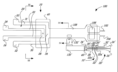
FIG. 1 shows an example of a MEMS switch 100 as improved. The switch
100 comprises two MEMS actuators 10, 10'. The MEMS switch 100 is used
5 to selectively close or open a circuit between a pair of contact terminals
102,
104 using a movable conductive member 106 mounted at the end of a
support arm 108. The contact terminals 102, 104 are mounted on a
substrate, as explained later in the text.
When the MEMS switch 100 is in a closed position, the contact terminals 102,
104 are electrically engaged, i.e. an electrical current or a signal may pass
between the two contact terminals 102, 104. This electrical engagement is
realized when the movable conductive member 106 electrically "shorts" the
pair of contact terminals 102, 104. The movable conductive member 106 can
be gold plated if desired.
Conversely, when the MEMS switch 100 is in an open position, the contact
terminals 102, 104 are not electrically engaged and no appreciable electrical
current or signal may pass between them.
FIGS. 2a and 2b are side views showing the actuators 10, 10' of FIG. 1 being
mounted in a cantilever fashion on a generic substrate 12. One example of
the substrate 12 is a silicon wafer. Other kinds of substrates can be used as
well.
CA 02679219 2009-08-26
WO 2008/113166 PCT/CA2008/000508
6
It should be noted that in FIG. 1 and certain subsequent figures, the support
arm 108 and the movable conductive member 106 appear transparent. This
is not necessarily to show any transparency of the parts. It only enhances the
visibility of those parts which would otherwise be eclipsed in these figures.
With the contact terminals 102, 104 such as those shown and a movable
conductive member 106, the switch 100 can conduct higher currents than
MEMS devices in which an electrical conducting path goes along a length of
the actuators 10, 10' themselves. This way, one can avoid using current
limiters. As a result, overall manufacturing costs of systems employing
MEMS switches can be significantly reduced and their performance can be
improved.
In the example shown in FIG. 1, each of the actuators 10, 10' comprises an
elongated hot arm 20, 20' having two spaced-apart portions 22, 22'. Each
spaced-apart portion 22, 22' is provided at one end with a corresponding
anchor pad 24, 24' connected to the substrate 12.
In each actuator 10, 10', the spaced-apart portions 22, 22' are substantially
parallel and connected together at a common end 26, 26' that is opposite the
anchor pads 24, 24' and overlying the substrate 12.
Each of the actuators 10, 10' also comprises an elongated cold arm 30, 30'
adjacent and substantially parallel to the corresponding hot arm 20, 20'. Each
cold arm 30, 30' has, at one end, anchor pads 32, 32' connected to the
substrate 12 and a free end 34, 34' that is opposite the corresponding anchor
CA 02679219 2009-08-26
WO 2008/113166 PCT/CA2008/000508
7
pads 32, 32'. The free ends 34, 34' overlie the substrate 12. The cold arm 30
of the first actuator 10 has two spaced-apart portions 31. It should be noted
that the use of the words "first" and "second" is only exemplary.
A dielectric tether 40, 40' is attached over the common end 26, 26' of the
portions 22, 22' of the hot arm 20, 20' and over the free end 34, 34' of the
cold
arm 30, 30'. The dielectric tether 40, 40' is provided to mechanically couple
the corresponding hot arm 20, 20' and cold arm 30, 30' so as to keep them
electrically independent, thereby maintaining them in a spaced-apart
relationship with a minimum spacing between them to avoid a direct contact
or a short circuit in normal operation as well as to maintain the required
withstand voltage, which voltage is proportional to the spacing between the
corresponding members 20, 30 and 20', 30'.
It should be noted that the maximum voltage used can be increased by
changing of the ambient atmosphere. For instance, the use of high electro-
negative gases as ambient atmosphere would increase the withstand voltage.
One example of this type of gases is Sulfur Hexafluoride, SF6.
The dielectric tether 40, 40' can be molded directly in place at the desired
location and be attached by direct adhesion. Direct molding further allows
having a small quantity of material entering the space between the parts
before solidifying. The dielectric tether 40, 40' may also be attached to the
hot arm 20, 20' and the cold arm 30, 30' in a different manner than the one
CA 02679219 2009-08-26
WO 2008/113166 PCT/CA2008/000508
8
shown in the figures. Moreover, the dielectric tethers 40, 40' can be
transparent as illustrated in some of the figures.
Each dielectric tether 40, 40' can be made entirely of a photoresist material.
A suitable material for that purpose, which is also easy to manufacture, is
the
material known in the trade as "SU-8". The SU-8 is a negative, epoxy-type,
near-UV photo resist based on EPON SU-8 epoxy resin (from Shell
Chemical). Other photoresist can be used as well, depending upon the
particular design requirements. Other possible suitable materials include
polyimide, spin on glass, oxide, nitride, ORMOCORETM, ORMOCLADTM or
other polymers. Moreover, combining different materials is also possible.
Providing each dielectric tether 40, 40' over the corresponding actuator 10,
10' can provide more flexibility of the tether material and a greater
reliability.
FIG. 3 is a cross-sectional view taken along line III-III in FIG. 1. It shows
that
the hot arm portions 22 of the first actuator 10 are slightly above the plane
of
the cold arm portions 31. The dielectric tether 40 is also visible in this
figure.
In use, when a control voltage is applied at the anchor pads 24, 24' of the
hot
arm 20, 20', a current travels into its first and second portions 22, 22'. In
the
various examples illustrated herein, the material(s) comprising the hot arms
20, 20' is/are sufficiently conductive so that it increases in length as it is
heated. The cold arms 30, 30', however, do not substantially exhibit such
elongation since no current is passing through them.
CA 02679219 2009-08-26
WO 2008/113166 PCT/CA2008/000508
9
In the example depicted in FIG. 1, when a control voltage is applied at anchor
pads 24 of the hot arm 20 of the first actuator 10, the member becomes
heated and the free end 34 of the first actuator 10 is deflected downwards
(towards the substrate) because of the heating induced elongation thereby
moving the support arm 108 from a neutral position to a deflected position.
Conversely, removing the control voltage results in the hot arm 20 cooling and
the support arm 108 returning to its original (neutral) position.
The second actuator 10' is designed and configured to deflect its free end 34'
sideways when a potential is applied to its anchor pads 24'. In this manner,
the first actuator 10 and the second actuator 10' move perpendicular to one
another. More specifically, the first actuator 10 moves in a direction
substantially perpendicular to the plane of the underlying substrate 12
(towards/away - down/up) while the second actuator 10' moves in a plane
that is substantially parallel to the surface plane of the substrate 12.
The second actuator 10' in the example shown in FIG. 1 includes a set of two
spaced-apart additional dielectric tethers 50'. These additional dielectric
tethers 50' are transversally disposed over the portions 22' of the hot arm
20'
and over the cold arm 30'. They adhere to these parts. These additional
dielectric tethers 50' provide additional strength to the hot arm 20', thereby
helping to prevent distortion of the hot arm 20' over time. Since the gap
between the parts is extremely small, the additional tethers 50' can reduce
the
risks of a short circuit happening between the two portions 22' of the hot arm
CA 02679219 2009-08-26
WO 2008/113166 PCT/CA2008/000508
20' or between the portion 22' of the hot arm 20' that is closest to the cold
arm
30' and the cold arm 30' itself by keeping them in a spaced-apart
configuration. Additionally, the additional dielectric tethers 50' can
alleviate
the fact that since the two portions 22' of the hot arm 20' are relatively
long,
5 they tend to distort when heated to produce the deflection, and this can
decrease the effective stroke of the second actuator 10'. Using one, two or
more additional dielectric tethers 50' can increase the rigidity of the
portions
22' of the hot arm 20', increase the stroke of the second actuator 10',
decrease the risks of shorts between the portions 22' of the hot arm 20' and
10 increase the breakdown voltage between the cold arm 30' and hot arm 20'.
The additional dielectric tethers 50' can be made of a material identical or
similar to that of the main dielectric tethers 40'. Small quantities of
materials
can be allowed to flow between the parts before solidifying in order to
improve
the adhesion. Furthermore, one or more holes or passageways (not shown)
can be provided in the cold arm 30' to receive a small quantity of material
before it solidifies to ensure a better adhesion.
The additional tethers 50' may also be provided at enlarge points 22' along
the length of the second actuator 10', as in the example of FIG. 1. These
enlarged points 22a' offer a greater contact surface and also contribute to
dissipate more heat when a current flows therein. Providing a larger surface
and allowing more heat to be dissipated can increase the actuator operating
lifetime.
CA 02679219 2009-08-26
WO 2008/113166 PCT/CA2008/000508
11
The free end 34' of the second actuator 10' holds an extension arm 130'. In
the illustrated example, the extension arm 130' is itself provided with a side
extension arm 132' at or near its free end. It should be noted that the hot
arm
20' and the cold arm 30' of the second actuator 10' can be made longer than
what is shown in FIG. 1. It is thus possible to omit the extension arm 130'
and
provide the side extension arm 132' directly on the side of the free end 34'.
The whole second actuator 10' can also be positioned differently with
reference to the first actuator 10.
FIG. 4 is a cross-sectional view taken along line IV-IV in FIG. 1. It shows
that
the side extension arm 132' of the illustrated example comprises a bottom peg
132a', whereas the support arm 108 comprises a corresponding hole 109.
FIGS. 5a through 5g schematically show an example of the relative
movement of the actuators 10, 10' when the MEMS switch 100 of FIG. 1 goes
from an "open position" to a "closed position", thereby closing the circuit
between the two contact terminals 102, 104 provided on the substrate 12. To
move from one position to the other, the actuators 10, 10' are operated in
sequence.
More particularly, FIGS. 5a and 5b show the initial position of the MEMS
switch 100. In FIGS. 5c and 5d, the hot arm 20 of the first actuator 10 is
activated so that the conductive member 106 is deflected downward toward
the underlying substrate. Then, as shown in FIG. 5e, the side extension arm
132' of the second actuator 10' is deflected to its right, parallel to the
surface
CA 02679219 2009-08-26
WO 2008/113166 PCT/CA2008/000508
12
of the underlying substrate, upon activation of its corresponding hot arm 20'.
At that point, a bottom peg 132a' is in registry with the hole 109 of the
support
arm 108, which are shown in FIG. 4.
FIG. 5f shows the effect of the control voltage in the first actuator 10 being
released, which causes the support arm 108 to engage the bottom side of the
side extension arm 132' of the second actuator 10' as it returns towards its
neutral position. The peg 132a' is then retained in the hole 109 (FIG. 4).
Then, as shown in FIG. 5g, the control voltage of the second actuator 10' is
released. Both actuators 10, 10' are then in a stable engagement and the
contact member 106 is pressed against the contact terminals 102, 104
provided on the substrate even if the base of the support arm 108 moves
slightly up when the control voltage is released. This closes the MEMS switch
100 and the contact terminals 102, 104 are electrically engaged together.
The MEMS switch 100 may be opened by reversing the above-mentioned
operations.
FIG. 6a illustrates another example of an improved MEMS switch 100. This
example is similar to the one illustrated in FIG. 1, with the exception that
it
comprises two second actuators 10' and no peg and hole arrangement. As
shown, the first actuator 10 is maintained in the closed position only by the
presence of the side extension arm 132' that is provided on one of second
actuators 10'. The two second actuators 10' move substantially parallel to the
surface of the substrate upon which they are disposed. In addition, they move
CA 02679219 2009-08-26
WO 2008/113166 PCT/CA2008/000508
13
in a direction that is substantially perpendicular to one another. In this
manner, once the first actuator 10 is moved into its deflected position, it is
held in that position through the effect of the two second actuators 10', one
of
the second actuators 10' securing the other of the second actuators 10'.
FIG. 6b shows that when the second actuators 10' of a same pair will be set
to their "closed" position, the side extension arm 132' of the second actuator
10' that is closer to the first actuator 10 is moved of a distance d'. This
distance d' is greater than a distance d between the tip of the side extension
arm 132' and the edge of the support arm 108 of the first actuator 10. FIG. 6c
is a schematic side view showing the contact member 106 of the support arm
108 being engaged over the contact terminals 102, 104 (only contact terminal
102 being shown) when the MEMS switch 100 in FIG. 6a is in the closed
position, i.e. with both actuators 10' being latched.
FIG. 7 illustrates another example of an improved MEMS switch 100. It
comprises the two opposite pairs of second actuators 10'. One of the second
actuators 10' of each pair is parallel to the first actuator 10 while the
other
second actuator 10' of each pair is perpendicular with reference to the first
actuator 10. One goal of this symmetrical positioning of the second actuators
10' is to have the same electrical contact pressure on each contact terminal
102, 104 provided on the substrate (not shown in FIG. 7).
FIG. 8 illustrates yet another example of an improved MEMS switch 100. In
this example, the base of the support arm 108 is electrically insulated from
its
CA 02679219 2009-08-26
WO 2008/113166 PCT/CA2008/000508
14
free end with a dielectric tether 110. This allows, for instance, providing a
potential between the anchor pads 32 of the "cold" arm 30 of the first
actuator
10. In this manner, a stiction effect between the contact terminals 102, 104
and the movable conductive member 106 on the first actuator 10 can be more
easily broken. A stiction effect can be generally defined as a retention force
urging the conductive member 106 to stay on the contact terminals 102, 104.
Microwelding is one possible cause of stiction, especially if the conductive
member 106 stays in contact with the contact terminals 102, 104 for a long
period of time. The "cold" arm 30 can then be temporally used as a "hot" arm
when a potential is applied at its actuator pads 32 so as to generate a
positive
force pushing up the conductive member 106 to break the contact. The "hot"
arm of the first actuator 10 would then be used as a "cold" arm at that
moment. The pushing force adds to the natural spring force of the first
actuator 10. This feature can be used with any of the other possible designs,
provided that electric insulation is provided at an appropriate location to
insulate the parts. The main dielectric tether 40 of the first actuator 10 can
also be used to insulate the support arm 108 from the cold arm 30 of the first
actuator 10. For instance, the support arm 108 can be provided as a separate
part that is not made integral with the cold arm 30.
FIG. 9 illustrates another example of an improved MEMS switch 100. The
first actuator 10 has two support arms 108a, 108b to support two movable
conductive members 106a, 106b. One movable conductive member 106a
can short the corresponding pair of contact terminals 102a, 104a. The other
CA 02679219 2009-08-26
WO 2008/113166 PCT/CA2008/000508
movable conductive member 106b can short the corresponding pair of contact
terminals 102b, 104b. Two second actuators 10' are used in the illustrated
example to maintain the circuits in a closed position. These second actuators
10' can also be used with other kinds of first actuator 10, for instance the
one
5 illustrated in FIG. 1.
It is understood that the above-described examples are illustrative only.
Numerous and various other arrangements and combinations can be made.