Note: Descriptions are shown in the official language in which they were submitted.
CA 02680043 2009-09-04
WO 2008/106764 PCT/CA2007/002238
SENSOR PIXELS, ARRAYS AND ARRAY SYSTEMS AND METHODS THEREFOR
CROSS-REFERENCE TO RELATED APPLICATIONS
[0001 ] This application claims the benefit of the filing dates of Canadian
Patent
Application No. 2,582,243 filed 3 Mar. 2007 under the title LOW NOISE HYBRID
ACTIVE-PASSIVE PIXEL FOR DIFFERENT SENSOR APPLICATIONS and Canadian
Patent Application No. 2,594,737 filed 13 Jul. 2007 under the title HIGH
SENSITIVITY
a-Si:H PHOTO TRANSISTOR WITH FLICKER NOISE REDUCTION FOR NEAR
INFRA_RED IN-VIVO BIO-MOLECULAR IMAGING. The content of the above patent
applications and Canadian Patent Application No. 2,564,239 filed 10 Oct. 2006
under title
LOW NOIST ACTIVE PIXEL SENSOR is hereby expressly incorporated by reference
into the detailed description hereof.
FIELD OF INVENTION
[0002] The present invention relates to imaging systems, sensor pixels, and
more
specifically to methods and systems for sensor pixels and applications
thereof.
BACKGROUND OF THE INVENTION
[0003] Sensor pixel circuits (sensor pixels) have many applications. For
example, when
used in pixel arrays as part of a pixel array system for reading out sensed
data, such pixel
array systems can be used as charge coupled devices (CCDs) for use in digital
cameras.
Sensor pixels, pixel arrays and pixel array systems also find use in
biomolecular and
biomedical imaging, chemical sensing and a wide range of other fields.
[0004] It is desirable to provide alternative circuits, arrays and systems. It
is also desirable
to provide alternative methods of operating existing circuits, arrays and
systems, and it is
desirable to provide methods of operating alternative circuits, arrays and
systems.
1
CA 02680043 2009-09-04
WO 2008/106764 PCT/CA2007/002238
SUMMARY OF THE INVENTION
[0005] In accordance with a first aspect of the present invention there is
provided a sensor
pixel. The sensor pixel includes an amplifying transistor having a first
terminal, a second
terminal and a gate terminal, the first terminal of the amplifying transistor
is coupled to a
first bias line. The pixel also includes a switch transistor having a first
terminal, a second
terminal and a gate terminal, the gate terminal of the switch transistor are
operated by a
control line. The pixel further includes a storage capacitor having a first
terminal and a
second terminal, the first terminal of the storage capacitor being coupled to
a second bias
line. The pixel additionally includes a sensor. The second terminal of the
amplifying
transistor and the first terminal of the switch transistor are coupled to at
least one data line.
The sensor, the second terminal of the storage capacitor, the second terminal
of the switch
transistor are coupled to the gate terminal of the amplifying transistor.
[0006] The at least one data line may include a first data line coupled to the
second
terminal of the amplifying transistor, and a second data line coupled to the
first terminal of
the switch transistor.
[0007] Each of the first and second bias lines and the data line may be used
at a
predetermined timing to bias the pixel.
[0008] In accordance with a second aspect of the present invention there is
provided a
method for operating a sensor pixel. The sensor pixel includes an amplifying
transistor
having a first terminal, a second terminal and a gate terminal; a switch
transistor having a
first terminal, a second terminal and a gate terminal; a storage capacitor
having a first
terminal and a second terminal; and a sensor. The first terminal of the
amplifying
transistor is coupled to a first bias line. The gate terminal of the switch
transistor is
operated by a control line. The first terminal of the storage capacitor is
coupled to a
second bias line. The second terminal of the amplifying transistor and the
first terminal of
the switch transistor are coupled to at least one data line. The sensor, the
second terminal
of the storage capacitor, and the second terminal of the switch transistor are
coupled to the
gate terminal of the amplifying transistor at a coupling node. The method
includes the
steps of at a first operating cycle, charging the coupling node; at a second
operating cycle,
changing the voltage of the coupling node by a sensor signal generated by the
sensor; and
2
CA 02680043 2009-09-04
WO 2008/106764 PCT/CA2007/002238
at a third operating cycle, applying a current or voltage to the at least one
data line and
operating on the first bias line and the second bias line.
[0009] In accordance with a third aspect of the present invention there is
provided a sensor
pixel. The sensor pixel includes a first amplifying transistor having a first
terminal, a
second terminal and a gate terminal, the first terminal of the first
amplifying transistor is
coupled to a first bias line. The sensor pixel also includes a second
amplifying transistor
having a first terminal, a second terminal and a gate terminal, the first
terminal of the
second amplifying transistor is coupled to a second bias line. The sensor
pixel further
includes a switch transistor having a first terminal, a second terminal and a
gate terminal,
the gate terminal of the switch transistor is operated by a control line. The
sensor pixel
additionally includes a storage capacitor having a first terminal and a second
terminal. The
sensor pixel further includes a sensor. The second terminal of the first
amplifying
transistor, the second terminal of the second amplifying transistor and the
first terminal of
the switch transistor are coupled to at least one data line. The sensor, the
second terminal
of the storage capacitor, and the second terminal of the switch transistor are
coupled to the
gate terminal of the first amplifying transistor and the gate terminal of the
second
amplifying transistor.
[0010] The at least one data line may include a first data line coupled to the
second
terminal of the first and second amplifying transistors, and a second data
line coupled to
the first terminal of the switch transistor. The first bias line and the
second bias line may
be alternately switched.
[0011 ] In accordance with a fourth aspect of the present invention there is
provided a
method for operating a sensor pixel. The sensor pixel includes a first
amplifying transistor
having a first terminal, a second terminal and a gate terminal; a second
amplifying
transistor having a first terminal, a second terminal and a gate terminal; a
switch transistor
having a first terminal, a second terminal and a gate terminal; a storage
capacitor having a
first terminal and a second terminal; and a sensor. The first terminal of the
first amplifying
transistor is coupled to a first bias line. The first terminal of the second
amplifying
transistor is coupled to a second bias line. The gate terminal of the switch
transistor is
operated by a control line. The second terminal of the first amplifying
transistor, the
3
CA 02680043 2009-09-04
WO 2008/106764 PCT/CA2007/002238
second terminal of the second amplifying transistor and the first terminal of
the switch
transistor are coupled to at least one data line. The sensor, the second
terminal of the
storage capacitor, the second terminal of the switch transistor are coupled to
the gate
terminal of the first and second amplifying transistors. The method includes
the steps of,
at a selecting cycle, selecting the pixel and, at a read out cycle,
alternately switching the
first bias line and the second bias line.
[0012] In accordance with a fifth aspect of the present invention there is
provided a
method for a sensor pixel having a first photo transistor and a second photo
transistor, each
having a first terminal, a second terminal and a gate terminal, the method
comprising the
steps of, at a first operating cycle, resetting the first and second photo
transistors and, at a
second operating cycle, reading sensed data from the first photo transistor
and the second
photo transistor, including alternately biasing the first terminals of the
first photo transistor
and the second photo transistor.
[0013] The step of reading may include sensing the second terminals of the
first photo
transistor and the second photo transistor. The step of resetting at the first
operating cycle
may include setting the gate terminals of the first photo transistor and the
second photo
transistor to a predetermined level.
[0014] The method may further include, at a third operating cycle, resetting
the first photo
transistor and the second photo transistor. The step of resetting the first
and second photo
transistors may include turning off the first and second transistors.
[0015] In accordance with a sixth aspect of the present invention there is
provided a
method for a sensor pixel in a sensor pixel array, the method including the
steps of any of
the methods for a sensor pixel of the other aspects, and, following reading
sensed data of
the first photo transistor and the second photo transistor of the pixel,
resetting the first
photo transistor and the second photo transistor of the pixel before reading
another pixel in
the array.
[0016] The pixel may be part of a pixel array in any method for a sensor pixel
of the other
aspects. The pixel array may be part of a pixel array system, and the method
may also
4
CA 02680043 2009-09-04
WO 2008/106764 PCT/CA2007/002238
include addressing individual pixels in the pixel array to perform the method
on each
pixel. The pixels may be addressed sequentially.
[0017] In accordance with a further aspect of the present invention there is
provided a
sensor pixel. The sensor pixel includes a first photo transistor and a second
photo
transistor, each having a first terminal, a second terminal and a gate
terminal. The gate
terminals of the first photo transistor and the second photo transistor are
coupled to a
control line. The first terminals of the first photo transistor and the second
photo transistor
are coupled to a first data line. The second terminal of the first photo
transistor is coupled
to a first bias line. The second terminal of the second photo transistor is
coupled to a
second bias line. The first bias line and the second bias line are alternately
switched
during readout cycle.
[0018] At least one of the first and second photo transistors maybe an
inverted staggered
a-Si:H photo-TFT. At least one of the first and second photo transistors may
include a
glass substrate with the gate deposited on the glass substrate; a-Si:Nx layer
and a-Si:H
layer deposited on the gate; a drain electrode and a source electrode
deposited on the a-
Si:H layer; and a passivation layer deposited on the source and drain
electrodes.
[0019] In accordance with another aspect of the present invention there is
provided a
method for a sensor pixel having a sensor, a switch transistor, a first
transistor, a second
transistor, and a storage capacitor. The transistor has a first terminal, a
second terminal
and a gate terminal. The method includes the steps of, at a first cycle,
charging the storage
capacitor; at a second cycle, integrating a sensor signal from the sensor by
the storage
capacitor; and, at a third cycle, reading sensed data from the first
transistor and the second
transistor, including alternately biasing the first terminals of the first
transistor and the
second transistor.
[0020] The step of reading may include sensing the second terminals of the
first transistor
and the second transistor. The step of reading comprises may include sensing
the first
terminal of the switch transistor and the second terminals of the first
transistor and the
second transistor; while, the sensor, the storage capacitor and the gate
terminals of the first
transistor and the second transistor are connected to the second terminal of
the switch
transistor.
CA 02680043 2009-09-04
WO 2008/106764 PCT/CA2007/002238
[0021 ] In accordance with an additional aspect of the present invention there
is provided a
sensor pixel array. The sensor pixel array includes a plurality of sensor
pixels in
accordance with any sensor pixel of the other aspects, wherein the plurality
of sensor
pixels are organized in an array.
[0022] In accordance with a further additional aspect of the present invention
there is
provided a sensor pixel array system. The system includes a plurality of
sensor pixels in
accordance with any sensor pixel of the other aspects, wherein the plurality
of sensor
pixels are organized in an array; an address driver to individually address
the sensor pixels;
and a read out circuit coupled to the sensor pixels to read out data sensed by
the sensor
pixels.
[0023] In accordance with a still further aspect of the present invention
there is provided a
method for a sensor pixel that includes circuitry to sense an environmental
condition and
to amplify and readout a signal representative of the sensed condition. Such
circuitry
includes two transistors to amplify separately the signal during readout. The
method
includes, during readout, alternately turning on a respective one of the
amplification
transistors of the sensor pixel circuitry and turning off the other
amplification transistor to
reduce flicker.
[0024] The method may further include turning the two transistors of the
sensor pixel
circuitry off except when reading out the signal from the circuitry to reduce
aging of the
transistor.
[0025] In accordance with a still additional aspect of the present invention
there is
provided a sensor pixel including a sensor, at least one transistor to amplify
output from
the sensor, and a storage capacitor to store charge based on amplified output
from the
transistor, wherein the storage capacitor is a variable capacitor.
[0026] The variable capacitor may be a metal-insulator-semiconductor having a
bias line
such that the bias condition of the capacitor may be changed to adjust the
capacitance of
the capacitor.
[0027] In accordance with a still further additional aspect of the present
invention there is
provided a sensor pixel including a sensor, at least one transistor to amplify
output from
6
CA 02680043 2009-09-04
WO 2008/106764 PCT/CA2007/002238
the sensor, and a storage capacitor to store charge based on amplified output
from the
transistor, wherein the sensor is a variable capacitor.
[0028] In accordance with another still further additional aspect of the
present invention
there is provided a sensor pixel including any of the sensor pixels in
accordance with any
sensor pixel of the other aspects herein that includes a capacitor, and the
capacitor is a
variable capacitor.
[0029] The variable capacitor may be a metal-insulator-semiconductor having a
bias line
such that the bias condition of the capacitor may be changed to adjust the
capacitance of
the capacitor.
[0030] The variable capacitor may be a storage capacitor of the sensor pixel.
The variable
capacitor may be a sensor of the sensor pixel. The variable capacitor may be
both a
storage capacitor and sensor of the sensor pixel.
[0031] In accordance with yet another aspect of the present invention there is
provided a
method for a sensor pixel including circuitry to sense an environmental
condition and to
amplify and readout a signal representative of the sensed condition. Such
circuitry
includes at least one transistor to amplify the signal during readout. The
method includes
turning the at least one amplification transistor of the sensor pixel
circuitry off except
when reading out the signal from the circuitry to reduce aging of the
transistor.
[0032] Other aspects of the present invention and detailed additional features
of the above
aspects will be evident based upon the detailed description, FIGS. and claims
herein.
BRIEF DESCRIPTION OF THE DRAWINGS
[0033] For a better understanding of the present invention and to show more
clearly how it
may be carried into effect, reference will now be made, by way of example, to
the
accompanying drawings that show the preferred embodiment of the present
invention and
in which::
[0034] FIG. 1 is a diagram illustrating a sensor pixel circuit in accordance
with an
embodiment of the present invention;
7
CA 02680043 2009-09-04
WO 2008/106764 PCT/CA2007/002238
[0035] FIG. 2 is a timing chart illustrating an example of waveforms applied
to the photo
pixel circuit of FIG. 1;
[0036] FIG. 3-A is a diagram illustrating an example of an array system
including the
sensor pixel of FIG. 1;
[0037] FIG. 3-B is a diagram illustrating another example of an array system
including the
sensor pixel of FIG. 1;
[0038] FIG. 4 is a diagram illustrating a sensor pixel circuit in accordance
with another
embodiment of the present invention;
[0039] FIG. 5 is a timing chart illustrating an example of waveforms applied
to the photo
pixel circuit of FIG. 4;
[0040] FIG. 6-A is a diagram illustrating an example of an array system
including the
sensor pixel of FIG. 4;
[0041 ] FIG. 6-B is a diagram illustrating an example of an array system
including the
sensor pixel of FIG. 4;
[0042] FIG. 7 is a diagram illustrating a sensor pixel circuit in accordance
with a further
embodiment of the present invention;
[0043] FIG. 8 is a timing chart illustrating an example of waveforms applied
to the pixel
circuit of FIG. 7;
[0044] FIG. 9 is a timing chart illustrating another example of waveforms
applied to pixel
sensor circuits;
[0045] FIG. 10 is a diagram illustrating a sensor pixel circuit in accordance
with a further
embodiment of the present invention;
[0046] FIG. 11 is a timing chart illustrating an example of waveforms applied
to the sensor
pixel circuit of FIG. 10;
8
CA 02680043 2009-09-04
WO 2008/106764 PCT/CA2007/002238
[0047] FIG. 12 is a timing chart illustrating another example of waveforms
applied to the
sensor pixel circuit of FIG. 10;
[0048] FIG. 13 is a diagram illustrating a sensor pixel circuit in accordance
with a further
embodiment of the present invention;
[0049] FIG. 14 is a timing chart illustrating an example of waveforms applied
to the sensor
pixel circuit of FIG. 13;
[0050] FIG. 15 is a diagram illustrating an example of an array system
including the sensor
pixel circuit of FIG. 13;
[0051 ] FIG. 16 is a diagram illustrating the structure of an inverted
staggered photo thin
film transistor (TFT) used as a photo-detector;
[0052] FIG. 17 is a graph showing an effect of bias on the responsivity of the
photo TFT;
[0053] FIG. 18 is a graph showing the photocurrent of the photo TFT as a
function of
illumination intensity for various gate biases;
[0054] FIG. 19 is a photomicrograph of the photo pixel circuit;
[0055] FIG. 20A is a graph showing waveforms in a read cycle of the photo
pixel circuit of
FIG. 13 for two different illumination conditions;
[0056] FIG. 20B is a graph showing the simulation results for the photocurrent
of the
photo pixel circuit of FIG. 13;
[0057] FIG. 21 is a diagram illustrating the setup for measuring the noise of
the photo
pixel circuit of FIG. 13;
[0058] FIG. 22 is a graph showing the measuring results by the measuring
environment of
FIG. 20;
[0059] FIG. 23 is a graph showing variation of a storage capacitance for a
capacitor
applicable to the sensor pixel;
9
CA 02680043 2009-09-04
WO 2008/106764 PCT/CA2007/002238
[0060] FIG. 24 is a graph showing the pixel performance using MIS-capacitor
gain for
extremely low intensity input signals (photon count);
[0061 ] FIG. 25 is a diagram illustrating an example of using a transistor as
the storage
capacitor.
[0062] FIG. 26 is a graph showing variation of a transistor-based storage
capacitance for a
capacitor applicable to the pixel; and
DETAILED DESCRIPTION
[0063] Embodiments of the present invention are described using a pixel
circuit having at
least one transistor. The transistor in the pixel circuit may be fabricated in
any
technologies, including CMOS (e.g., MOSFET), NMOS, PMOS, amorphous silicon,
nano/micro crystalline silicon, poly crystalline, oxide semiconductors, and
liquid-printed
and vacuum deposited organic technology. A pixel array having the pixel
circuit may be
an active matrix image sensor array, and may be, for examples, but not limited
to, used for
medical applications from imaging at tissue and organ levels to molecular and
cellular
levels. The examples include applications for large area multi-modal
biomedical and other
x-ray imaging (when coupled to a scintillation layer) to optical bio-molecular
imaging,
including that of fluorescence-based bio-arrays. The examples include
sensitive
applications including single event detector (single photon, single DNA).
[0064] In the description below, "pixel" and "pixel circuit" are used
interchangeably. In
the description below, "signal" and "line" may be used interchangeably as
appropriate in
the context. In the description below, the terms "line" and "node" may be used
interchangeably as appropriate in the context. In the description below, the
terms "select
line" and "address line" may be used interchangeably. In the description
below, "connect
(or connected)"and "couple (or coupled)" may be used interchangeably, and may
be used
to indicate that two or more elements are directly or indirectly in physical
or electrical
contact with each other.
[0065] Included in this description are a variety of novel pixel circuits that
may be used to
exploit the flicker reduction, aging reduction, aging compensation, and trap-
assisted
absorption features and other features described herein; however, it is to be
recognized that
CA 02680043 2009-09-04
WO 2008/106764 PCT/CA2007/002238
these circuits do not have to utilize these features and can be operated
beneficially in
alternative manners. Methods of biasing pixel circuits will be described
herein to provide
features such as flicker reduction, aging reduction and aging compensation. It
is to be
recognized that such methods may be applied to the novel pixel circuits
described herein;
while, the methods may also be applied to alternate pixel circuits including
existing pixel
circuits. Similarly, trap-assisted absorption may be utilized in alternative
pixel circuits
including existing pixel circuits.
[0066] Pixel circuits described herein will be described with reference to
photoelectric
sensor pixel circuits; however, it is to be recognized that other sensors and
transistors for
such sensors, such as chemical sensors, temperature sensors, biomedical
transducers,
optical sensors, and direct x-ray sensors producing electric charge to be
readout of the
pixel circuits described herein and other pixel circuits to which the features
herein can be
applied. Such other sensors may for example be mechanical or chemical sensors,
as
appropriate. As is known in the art, such sensors may themselves be
capacitors.
[0067] FIG. 1 illustrates a sensor pixel circuit in accordance with an
embodiment of the
present invention. The sensor pixel circuit 10 of FIG. 1 includes an
amplifying transistor
12, a switch transistor 14, a storage capacitor 16, and a sensor 18. The
transistors 12 and
14 are, for example, but not limited to, TFTs (hereinafter referred to as TFT
12, TFT 14,
respectively), and each has first and second terminals and a gate terminal. In
this
embodiment, the pixel circuit 10 is a 2-TFT sensor pixel circuit and may form
an active
matrix array. The sensor 18 may be, for example, but not limited to, a photo
detector,
biomedical transducer, chemical sensor, temperature sensor, or direct x-ray
sensor. It is
well understood by one of ordinary skill in the art that the NMOS transistor
in the pixel 10
can be replaced with a PMOS transistor using the concept of complementary
circuit
design.
[0068] The first terminal of TFT 12 is connected to a data line RDATA, and the
second
terminal of TFT 12 is connected to a bias line VB2. The first terminal of TFT
14 is
connected to a data line WDATA, and the second terminal of TFT 14 is connected
to the
gate terminal of TFT 12 at node A1. The gate terminal of TFT 14 is connected
to a write
11
CA 02680043 2009-09-04
WO 2008/106764 PCT/CA2007/002238
line WR. The storage capacitor 16 is connected to the node A1 and a bias line
VB1. The
sensor 18 is connected to the node Al.
[0069] The sensor pixel circuit 10 is biased using a biasing voltage,. Also,
it can be biased
with a biasing current resulting in that mismatching and aging effects of the
sensor pixel
circuit is reduced. FIG. 5 describes the current biasing. The current is
applied to the pixel
during the first driving cycle.
[0070] One example of operating cycles for the sensor pixel circuit 10 is
illustrated in FIG.
2. Referring to FIGS. 1-2, the operation of the sensor pixel circuit 10
includes three
operating cycles 22, 24, and 26. This driving scheme provides low noise, high
sensitive,
and low power (consumption) sensor.
[0071 ] During the first operating cycle 22, the node A 1 is charged to a
biasing voltage
(VR) by setting WDATA to VP and setting WR to high. During the second
operating
cycle 24, a sensor signal generated by the sensor 18 changes the voltage at
node Al.
During the third operating cycle 26, a current/voltage is applied to RDATA
while the bias
lines VB 1 and VB2 go to VI and V2 respectively to turn on TFT 12. V 1 and V2
are
defined based on the pixel bias conditions and parasitic capacitances.
Therefore, the
modulated voltage at node A1 changes the voltage/current at node B1
correspondingly.
[0072] The operation of FIG. 2 includes the second operating cycle 24 and the
third
operating cycle 26. However, in another example, the second and third
operating cycles
24 and 26 may be repeated with and without sensor effects, correlated double
sampling
(CDS), to manage the leakage current, reset noise, and low frequency noise
effects.
[0073] FIG. 3-A illustrates an example of an array structure including the
sensor pixel
circuit 10 of FIG. 1. The sensor pixel array system 30 of FIG. 3-A has
programming and
readout functions for a sensor pixel array 32. The sensor pixel array 32
includes a plurality
of sensor pixel circuits corresponding to that of FIG. 1. The sensor pixel
array system 30
further includes an address driver 34 and a read out circuit 36. .
[0074] In FIG. 3-A, VB 1[i] corresponds to VB 1 of FIG. 1, VB2[i] corresponds
to VB2 of
FIG. 1, RDATA[i] corresponds to RDATA of FIG. 1, and WDATA[i] corresponds to
WDATA of FIG. 1.
12
CA 02680043 2009-09-04
WO 2008/106764 PCT/CA2007/002238
[0075] In FIG. 3-A, APS 38-A and PPS 38-B switches connect RDATA[i] or
WDATA[i]
to the readout block for active or passive readout respectively. However, one
can share the
readout block between WDATA[i] and RDATA[i+1] or between WDATA[i] and
RDATA[i-1]. Also, Rd 38-C switch connects the reset voltage to the WDATA [i].
This
enable fast resetting for real time imaging.
[0076] For current biasing, APS 38-A and PPS-38B are both close and a biasing
current is
applied to the circuit through Rd 38-C. However, for voltage biasing, APS 38-A
and PPS
38-B can be open.
[0077] FIG. 3-B illustrates another example of an array structure including
the sensor pixel
circuit 10 of FIG. 1. The sensor pixel array system 30 of FIG. 3-B has
programming and
readout functions for a sensor pixel array 32. The sensor pixel array 32
includes a plurality
of sensor pixel circuits corresponding to that of FIG. 1. The sensor pixel
array system 30
further includes an address driver 34 and a read out circuit 36.
[0078] In FIG. 3-B, VB1 [i] corresponds to VBI of FIG. 1, VB2[i] corresponds
to VB2 of
FIG. 1, and RDATA[i] corresponds to RDATA of FIG. 1, and WDATA corresponds to
WDATA of FIG. 1.
[0079] FIG. 4 illustrates a sensor pixel circuit in accordance with another
embodiment of
the present invention. The sensor pixel circuit 40 of FIG. 4 includes an
amplifying
transistor 42, a switch transistor 44, a storage capacitor 46, and a sensor
48. The
transistors 42 and 44 are, for example, but not limited to, TFTs (hereinafter
referred to as
TFT 42, TFT 44, respectively), and each has first and second terminals and a
gate terminal.
In this embodiment, the pixel circuit 40 is a 2-TFT sensor pixel circuit and
may form an
active matrix array. The sensor 48 may be similar or the same as the sensor 18
of FIG. 1.
It is well understood by one of ordinary skill in the art that the NMOS
transistor in the
pixel 40 can be replaced with a PMOS transistor using the concept of
complementary
circuit design.
[0080] The first terminal of TFT 42 is connected to a data line DATA, and the
second
terminal of TFT 42 is connected to a bias line VB2. The first terminal of TFT
44 is
connected to the data line DATA, and the second terminal of TFT 44 is
connected to the
13
CA 02680043 2009-09-04
WO 2008/106764 PCT/CA2007/002238
gate terminal of TFT 42 at node A2. The gate terminal of TFT 44 is connected
to a write
line WRITE. The storage capacitor 46 is connected to the node A2 and a bias
line VB 1.
The sensor 48 is connected to the node A2. In this pixel circuit 40, one DATA
line is used
instead of two data lines WDATA and RDATA of FIG. 1.
[0081 ] The sensor pixel circuit 40 is biased using a biasing current,
resulting in that
mismatching and aging effects of the sensor pixel circuit is reduced. The
biasing current is
applied to the pixel 40during the first operating cycle, while SEL is high, a
current is
applied to data[i] and the gate voltage.
[0082] One example of operating cycles for the sensor pixel circuit 40 is
illustrated in FIG.
5. Referring to FIGS. 4-5, the operation of the sensor pixel circuit 40
includes three
operating cycles 52, 54, and 56. This driving scheme provides a low noise,
high
sensitivity, and low power (consumption) sensor.
[0083] During the first operating cycle 52, the node A2 is charged to a
biasing voltage
(VP). In this pixel circuit 40, a current can be used for biasing to manage
the mismatches,
aging effects and temperature variations. Hence, VB1 and VB2 change to Vl1 and
V21 to
turn on TFT 42 for biasing with a current. VP/IP for DATA in FIG. 5 indicates
that the
biasing signal can be either a voltage (VR) or a current (IR). If a biasing
voltage is used,
V11 can be zero and V21 can be VR. Thus, TFT 42 (T1) will be off resulting in
lower
power consumption and lower leakage. If a biasing current is used. V 11 can be
higher than
zero, and V21 is zero. Here, TFT 42 (Tl) is ON and allows the biasing current
passes
through it. Also, the pixel may be reset by a larger current than actual
required current to
improve the settling time.
[0084] During the second operating cycle 54, a sensor signal generated by the
sensor 48
changes the voltage at node A2. During the third operating cycle 56, a
current/voltage is
applied to DATA while the bias lines VB 1 and VB2 goes to V 12, V22
respectively to turn
on TFT 42. V12 is zero and V22 is VR and so T1 is off during this cycle, thus
power
consumption drops and T1 does not age. Also, if a biasing current is used
during previous
operating cycle 54, by bringing VB 1 from V 11 (non-zero) to V 12 (zero), the
pixel current
is reduced to the required current.
14
CA 02680043 2009-09-04
WO 2008/106764 PCT/CA2007/002238
[0085] During the third operating cycle 56, VB2 is zero and so T1 is ON. Since
it gate
voltage is modified by the sensor, its drain current changes accordingly.
Thus, T1 current
can be read as a representative of the sensor signal.
[0086] The operation of FIG. 5 includes the second operating cycle 54 and the
third
operating cycle 56. However, in another example, the second and third
operating cycles
54 and 56 may be repeated with and without sensor effects, correlated double
sampling
(CDS), to manage the leakage current and low frequency noise effects.
[0087] A pixel array system for an array having the sensor pixel 40 of FIG. 4
may be
similar to the pixel array system 30 of FIG. 3. FIG. 6-A illustrates one
example of an array
structure for the pixel 40 for voltage biasing. FIG. 6-B illustrates another
example of an
array structure for the pixel 40 for current biasing.
[0088] FIG. 7 illustrates a sensor pixel circuit in accordance with a further
embodiment of
the present invention. The pixel circuit 60 of FIG. 7 includes two amplifying
transistors
72 and 74, a switch transistor 76, a storage capacitor 78, and a sensor 80.
The transistors
72, 74, and 76 are, for example, but not limited to, TFTs (hereinafter
referred to as TFT
72, TFT 74, TFT 76, respectively), and each has first and second terminals and
a gate
terminal. The pixel circuit 60 is a 3-TFT sensor pixel circuit and may form an
active
matrix array. The sensor 80 may be similar or the same as the sensor 18 of
FIG. 1. It is
well understood by one of ordinary skill in the art that the NMOS transistor
in the pixel 60
can be replaced with a PMOS transistor using the concept of complementary
circuit
design.
[0089] The first terminal of TFT 72 is connected to a data line Idata[i], and
the second
terminal of TFT 72 is connected to a bias line VB2. The first terminal of TFT
74 is
connected to the data line Idata[i], and the second terminal of TFT 74 is
connected to a
bias line VB3. The first terminal of TFT 76 is connected to a data line
Vdata[i], and the
gate terminal of TFT 76 is connected to a select line SEL. The second terminal
of TFT 76
is connected to the gate terminals of TFTs 72 and 74 at node A3. The storage
capacitor 78
is connected to VB I. The storage capacitor 78 and the sensor 80 are connected
to node A3.
"i" represents, for example, the ith column in an array for the pixel.
CA 02680043 2009-09-04
WO 2008/106764 PCT/CA2007/002238
[0090] One example of operating cycles for the pixel circuit 60 is illustrated
in FIG. 8.
The operating cycles of the pixel circuit 60 includes a first operating cycle
82, a second
operating cycle 84, and a third operating cycle 86. The third operating cycle
86 is a read
cycle (or readout cycle, hereinafter referred to as read cycle).
[0091 ] The switch biasing technique is applied during the read cycle 86. The
switch
biasing technique reduces the low frequency noise. This driving technique
provides low
noise, high sensitivity and low power detection.
[0092] Referring to FIGS. 7 and 8, during the first operating cycle 82, the
storage capacitor
78 is charged to a biasing voltage (VR) by setting SEL, Vdata[i], VB1, VB2,
VB3, Idata
[i] to a high voltage (VH), VR, zero, VR, VR, and VR, respectively. If a
biasing current is
used, the storage capacitor 78 is charged to a biasing voltage (VR) by setting
SEL,
Vdata[i], VB 1, VB2, VB3, Idata [i] to a high voltage (VH), VR, a voltage
larger than zero
, zero, zero, and VR, respectively. This biasing condition provides for low
leakage
current, longer TFT lifetime, and lower power consumption. However, the
biasing
condition can change to other values as well.
[0093] During the second cycle 84, SEL, Vdata[i], VB1, VB2, VB3, Idata [i] are
set to a
low voltage (VL), VR, zero, VR, VR, and VR respectively. This biasing
condition
provides for low leakage current, longer TFT lifetime, and lower power
consumption.
During the second cycle 84, the sensor signal from the sensor 80 is integrated
by the
storage capacitor 78.
[0094] During the read cycle 86, VB2 and VB3 are set to be high and low,
alternately.
During the readout cycle 86, TFTs 72 and 74 turn on sequentially. Thus, the
output signal
of Idata[i] is not affected by the sync filter induced by the switch biasing
and it is
essentially equivalent to a single TFT with a DC bias.
[0095] In FIG. 7, the sensor pixel circuit 60 includes two amplifying
transistors 72 and 74.
However, in another embodiment, the sensor pixel circuit may use one TFT (TFT
72 or
TFT 74 of FIG. 7) to improve the aperture ratio and use a higher bias voltage
to
compensate for the gain lost by the switch biasing technique. Thus only one
bias line
VB2 (or VB3) is used. In this case, VB2 is oscillated as shown in FIG. 8. On
the other
16
CA 02680043 2009-09-04
WO 2008/106764 PCT/CA2007/002238
hand, the noise is reduced significantly due to the reduction of carrier
trapping/de-trapping
phenomena intrinsic to most transistors. Moreover, the lifetime of the pixel
is improved as
well.
[0096] The pixel circuits 60, 40, and 10 can work in hybrid mode which means
it can be
passive or active. For passive operation, VB2 and VB3 are chosen to be the
voltage
applied to Idata and so they are OFF as shown in FIG. 9 Therefore, the
integrated signal
can be read back through Vdata. For active operation, Here, data[i] is Wdata
for pixel
circuit 10, DATA for pixel circuit 40 and Vdata[i] for pixel circuit 60.
[0097] During the first operating cycle 92, storage capacitor is reset to a
biasing voltage
(VR). During the second operating cycle 94, the sensor signal is integrated by
the storage
capacitor. During the third operating cycle 96, the integrated signal is
readout through
data[i].
[0098] An array structure for the pixel 60 of FIG. 7 may be the same as that
of FIG. 3A or
FIG. 3B.
[0099] FIG. 10 illustrates a sensor pixel circuit in accordance with a further
embodiment
of the present invention. The sensor pixel circuit 100 of FIG. 10 includes two
amplifying
transistors 112 and 114, a switch transistor 116, a storage capacitor 118, and
a sensor 120.
The transistors 112, 114, and 116 are, for example, but not limited to, TFTs
(hereinafter
referred to as TFT 112, TFT 114, TFT 116, respectively), and each has first
and second
terminals and a gate terminal. The pixel circuit 100 is a 3-TFT sensor pixel
circuit and
may form an active matrix array. The sensor 120 may be similar or the same as
the sensor
18 of FIG. 1 It is well understood by one of ordinary skill in the art that
the NMOS
transistor in the pixel 100 can be replaced with a PMOS transistor using the
concept of
complementary circuit design.
[0100] The first terminal of TFT 112 is connected to a data line data[i], and
the second
terminal of TFT 112 is connected to a bias line VB2. The first terminal of TFT
114 is
connected to the data line data[i], and the second terminal of TFT 114 is
connected to a
bias line VB3. The first terminal of TFT 116 is connected to the data line
data[i], and the
gate terminal of TFT 116 is connected to a select line SEL. The second
terminal of TFT
17
CA 02680043 2009-09-04
WO 2008/106764 PCT/CA2007/002238
116 is connected to the gate terminals of TFTs 112 and 114 at node A4. The
first terminal
of the capacitor 118 is connected to VB 1. The storage capacitor 118 and the
sensor 120 are
connected to node A4. "i" represents, for example, the ith row in an array for
the pixel.
[0101] Examples of operating cycles for the pixel circuit 100 are illustrated
in FIG. 11
(voltage biasing) and FIG. 12 (current biasing). The operating cycles of the
pixel circuit
100 includes a first operating cycle 122, a second operating cycle 124 and a
third operating
cycle 126. The third operating cycle 126 is a read cycle (or readout cycle.).
[0102] The switch biasing technique is applied during the read cycle 126. The
switch
biasing technique reduces the low frequency noise. It is also able to control
the effect of
leakage current by reducing the drain-source voltage to zero as described
below. This
driving technique provides low noise, high sensitivity and low power
detection.
[0103] Referring to FIGS. 11 and 12, during the first operating cycle 122, the
storage
capacitor 118 is charged to a biasing voltage (VR) by applying a voltage or
current to the
data line data[i]. When using current as the biasing signal, VB2 and VB3 are
set to be zero
during the first operating cycle 122. When using voltage as the biasing
signal, VB2 and
VB3 can be as the voltage of data[i] to reduce power consumption.
[0104] During the second cycle 124, SEL, data[i], VB1, VB2, and VB3 are set to
a high
voltage (VH), reset voltage (VR), zero, VR, and VR respectively. For current
biasing
(FIG. 12), SEL, data[i], VB1, VB2, and VB3 are set to a high voltage (VH),
reset voltage
(VR), VB( > zero), zero, and zero respectively. During the second cycle 124,
the sensor
signal from the sensor 120 is integrated by the storage capacitor 118.
[0105] During the read cycle 126, TFTs 112 and 114 turn on sequentially. Thus,
the
output signal of TFT 112 (T1) and TFT 114 (T2) is not affected by the sync
filter caused
by the switch biasing and it is essentially equivalent to a single TFT with a
DC bias.
[0106] In FIG. 10, the sensor pixel circuit 100 includes two amplifying
transistors 112 and
114. However, in another embodiment, the sensor pixel circuit may use one TFT
(TFT
112 or TFT 114 of FIG. 10) to improve the aperture ratio and use a higher bias
voltage to
compensate for the gain lost by switch biasing technique. In this case, only
one bias line
VB2 (or VB3) is used, and VB2 (VB3) is oscillated as shown in FIG. 11 or 12.
On the
18
CA 02680043 2009-09-04
WO 2008/106764 PCT/CA2007/002238
other hand, the noise is reduced significantly due to the reduction of carrier
trapping/de-
trapping phenomena intrinsic to most transistors. Moreover, the lifetime of
the pixel is
improved as well.
[0107] The pixel 100 can work in hybrid mode which means it can be passive or
active.
For passive operation, VB2 and VB3 are chosen to be the voltage applied to
data[i] and so
they are OFF as shown in FIG. 12. Therefore, the integrated signal can be read
back
through data[i]. For active operation,
[0108] A pixel array system for an array having the sensor pixel 100 of FIG.
10 may be the
same as that of FIG. 6-A or 6-B.
[0109] FIG. 13 illustrates a sensor pixel circuit in accordance with a further
embodiment
of the present invention. The sensor pixel circuit 130 of FIG. 13 includes two
amplifying
transistors 132 and 134. The transistors 132 and 134 are photo transistors,
for example,
but not limited to, photo TFTs (hereinafter referred to as TFT 132, TFT 134,
respectively),
and each has first and second terminals and a gate terminal. The pixel circuit
130 is a 2-
TFT photo pixel circuit and may form an active matrix array. It is well
understood by one
of ordinary skill in the art that the NMOS transistor in the pixel 130 can be
replaced with a
PMOS transistor using the concept of complementary circuit design. Again, the
photo
transistors may be other forms of transistor as mentioned previously to sense
other
environmental conditions, such as for example temperature, x-rays or
chemicals.
[0110] The first terminal of TFT 132 is connected to a data line Idata[i], and
the second
terminal of TFT 132 is connected to a bias line VB1. The first terminal of TFT
134 is
connected to the data line Idata[i], and the second terminal of TFT 134 is
connected to a
bias line VB2. The gate terminal of each TFT is connected to a select line VB.
VB is a
bias voltage connected to a DC voltage; however, in some applications an AC
signal can
be applied to it as well.
[0111 ] One example of operating cycles for the pixel circuit 130 is
illustrated in FIG. 14.
Referring to FIGS. 13-14, the operation of the photo pixel circuit 130
includes tow
operating cycles 142 and 144. The operating cycles 142 and 146 are reset
cycles. The
19
CA 02680043 2009-09-04
WO 2008/106764 PCT/CA2007/002238
second operating cycle 144 is an readout cycle. It is noted that an AC signal
is illustrated
for VBl and VB2 in FIG.14 for the sake of generality.
[0112] The switch biasing technique is applied during the second operating
cycle 144.
The switch biasing technique reduces the low frequency noise. This driving
technique
provides low noise, high sensitivity and low power consumption.
[0113] During the first operating cycle 142, the drain-source (VDs) and gate-
source (VGS)
voltages are zero to reduce electrical stress for increased stability and
lifetime by setting,
for example, Idata[i]=15V, VB=15V, VB1=15V and VB2=15V. Moreover, the leakage
current is zero since VDs and Vcs are zero, leading to relatively lower cross
talk from
adjacent pixels in the same column.
[0114] During the second operating cycle 144, the voltage level of each VB 1
and VB2 is
switched. TFT 132 and TFT 134 are turned on and off alternately, providing
current to
Idata[i] in turn while their channel conductance is modulated as a result of
optical
interaction. Thus, the output signal of T1 and T2 is not affected by any sync
filter induced
by using a pulse signal in the switch biasing; while the signal is otherwise
essentially
equivalent to the output of a single TFT with a DC bias.
[0115] During the third operating cycle 146, VB1 and VB2 are set to VR (e.g.
15V). Idata
is set to VR and VB is set to zero. Thus, Tl and T2 experience no stress
resulting in
longer lifetime and more stability.
[0116] In FIG. 13, the sensor pixel circuit 130 includes two photo transistors
132 and 134.
However, in another embodiment, the sensor pixel circuit may use one photo TFT
alone
(TFT 132 or TFT 134) to improve the aperture ratio and use a higher bias
voltage to
compensate for gain lost by alternating the switch biasing. Again, only one
bias line VB 1
(or VB2) is used. In this case, VB 1 is oscillated as shown in FIG. 13.
[0117] FIG. 15 illustrates an example of an array structure including the
photo pixel circuit
130. The pixel array system 150 of FIG. 15 includes a photo pixel array 152,
an address
driver 154 and a read out circuit 156. The photo pixel array 152 includes a
plurality of
photo pixel circuits, each corresponding to that of FIG. 13. In FIG. 15, four
pixel circuits
(2x2 array structure) are shown as an example.
CA 02680043 2009-09-04
WO 2008/106764 PCT/CA2007/002238
[0118] In FIG. 15, VB 1[i] (i=l, 2, ...) represents a bias line for the ith
row and corresponds
to VB1 of FIG. 15; VB2[i] represents another bias line for the ith row and
corresponds to
VB2 of FIG. 13; and Idata [j] (j=1, 2, ..) represents a data line for the jth
column and
corresponds to Idata[i] of FIG. 13. VB, VB 1[i] and VB2[i] are driven by the
address
driver 154. Idata[j] is read by the read out circuit 156.
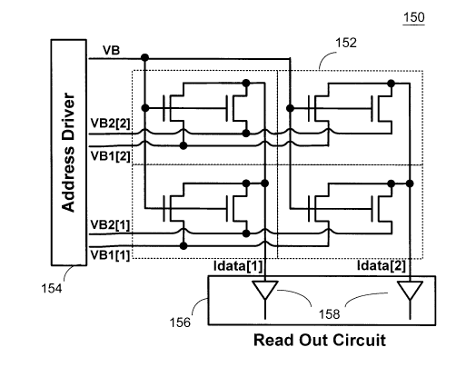
[0119] A row is selected by applying a pulse to its corresponding VB1 and VB2
lines (e.g.
VB 1[ 1] and VB2 [ 1]). The output current of each pixel in a selected row is
read out by a
trans-resistance or charge amplifier 158.
[0120] The sensor pixel circuit 130 and its operation scheme can provide high
responsivity
to near infra-red (NIR) and ultra-violet (UV) wavelengths critical for a
variety of imaging
applications. One important requirement for in-vivo bio-molecular imaging
applications,
can be sensitivity to near infra-red (NIR, 700-900 nm). This region of the
spectrum
enables penetration through tissue, to provide more accurate diagnostics.
Sensitivity to
UV provides a better choice of better quantum efficiency scintillation layers
for x-ray
imaging applications, besides direct UV sensing/imaging applications. The
particular
structure of the circuit 130 utilizing an a-Si: H imager provides sensitivity
in this region.
Also, the sensitivity is amplified utilizing the biasing herein.
[0121 ] FIG. 16 illustrates the structure of an example photo-thin film
transistor (TFT) used
as a photo-detector. As will be discussed below, the TFT 160 exhibits some
trap-assisted
absorption. Other TFTs can be structured to exhibit trap-assisted absorption.
Such TFTs
are particularly well suited to use in the pixel circuits described herein as
they can result in
smaller trapping time and consequently larger current. However, it is not
necessary to use
trap-assisted TFTs generally, nor this particular TFT 160, to take advantage
of other
techniques described herein, such as flicker reduction and TFT aging effect
reduction or
compensation. Other TFTs could be used when taking advantage of flicker
reduction and
aging effect reduction or compensation. TFT 160 of FIG. 16 includes a glass
substrate
162, a gate 164 deposited on the glass substrate 162, a-Si:Nx layer 166 and a-
Si:H layer
168 deposited on the gate 164, a drain electrode 170 and a source electrode
172 deposited
on the a-Si:H layer 168, and a passivation layer 174 deposited on the source
and drain
21
CA 02680043 2009-09-04
WO 2008/106764 PCT/CA2007/002238
electrodes 170 and 172. TFT 160 is exposed to photons 176 through the
passivation layer
174.
[0122] TFT 160 is an inverted staggered a-Si:H photo-TFT with 300 nm a-Si:Nx
layer 166
and 50 nm a-Si:H layer 168 fabricated using plasma enhanced chemical vapor
deposition
(PECVD). The aspect ratio of TFT 160 is 800 pm/23 m.
[0123] To reduce the effects of TFT aging on photocurrent (lillumination -
Idark), the dark
current is extracted before each measurement. As the gate voltage passes the
sub-
threshold regime, the responsivity to red illumination increases as shown in
FIG. 17.
[0124] FIG. 17 illustrates an effect of bias on the responsivity of the a-Si:H
photo-TFT
160 of FIG. 16. In FIG. 17, "VGs" represents the gate-source voltage of the
photo-TFT,
and "VDs" represents the drain-source voltage of the photo-TFT. The
responsivity of the
Si:H TFT is extracted by using an arc lamp (for example, an arc lamp sold
under the
trademark Oriel 66181) in series with a monochromator (for example, a
monochromator
sold under the trademark Oriel 77200), both calibrated with a silicon sensor
(for example,
a sensor sold under the trademark Newport 818-UV). The measured photocurrents
are
normalized to the photocurrent at 500-nm.
[0125] Referring to FIGS. 16-17, this is most likely due to trap-assisted
absorption in
which the photons are absorbed by the trapped electrons resulting in a smaller
trapping
time and consequently larger current. Also, the TFT photo-sensor provides high
sensitivity to the ultra violet range.
[0126] FIG. 18 illustrates the photocurrent of the TFT 160 as a function of
illumination
intensity for various gate biases. In FIG. 18, "Vcs" represents the gate-
source voltage of
the photo-TFT, and "VDs" represents the drain-source voltage of the photo-TFT.
The
illumination is generated by a red LED (for example, an LED sold under the
trademark
Avago Tech. HLMP-1301) with a peak at 635-nm wavelength. The sensitivity of
photo-
TFT 160 increases as the gate voltage increases. The photocurrent is
significantly high (>
50 nA) even at low intensities which is critical for high dynamic range, high
precision
imaging.
22
CA 02680043 2009-09-04
WO 2008/106764 PCT/CA2007/002238
[0127] Referring to FIGS.16-18, a photo pixel circuit 130 of FIG. 13 having
the TFT
structure 160 can be utilized as a bio-molecular pixel circuit. Although the
structure 160
of FIG. 16 can be used for any TFTs herein, the biasing techniques and age
effect
reduction and compensation techniques described herein can be used with other
TFT
structure as well as appropriate. In this embodiment, the pixel circuit 130
with the TFT
160 is designed and operated to deploy trap-assisted absorption in the TFT
while lowering
the 1/f noise and aging. These are attributes which can be exploited for
various other
sensing architectures for a variety of other imaging applications.
[0128] The photo pixel circuit 130 having TFT structure 160 shows enhanced
responsivity
of an a-Si:H thin film transistor (photo-TFT) to the near-infrared (NIR) and
ultra-violate
(UV) range of the optical spectrum by a means of trap-assisted absorption.
Because the
responsivity to UV is improved, it enables extensions of the imaging space to
large area
UV sensing and imaging.
[0129] A flicker noise (1/f) of the pixel is reduced by adopting the switch
biasing
technique : As the pixel provides for large in-pixel amplification, the
integration time is
diminished, limiting background noise stemming from dark current. Large in-
pixel
amplification results from applying alternating biasing to the transistors (T1
and T2) where
the transistors (TI and T2) are each amplification and sensing elements
[0130] The pixel circuit 130 having TFT structure 160 is designed and operated
to deploy
trap-assisted absorption in the TFT while lowering the 1/f noise and aging.
These are
attributes which can be exploited for various other sensing architectures for
a variety of
other imaging applications.
[0131 ] The technique applied to the pixel circuit 130 provides an economical
solution to
imaging as the image sensor and readout technique can be implemented in
standard
amorphous silicon flat panel technology.
[0132] FIG. 19 is a photomicrograph of an example integrated circuit
implementation of
the photo pixel circuit 130 assembled from discrete TFTs for test purposes. It
is to be
recognized that this is an example integrated circuit embodiment only and
other
embodiments can take on different forms as will be evident to those skilled in
the art..
23
CA 02680043 2009-09-04
WO 2008/106764 PCT/CA2007/002238
[0133] FIGS. 20A-21B show simulation conditions and the corresponding results.
The
waveforms of the read cycle (e.g., 144 of FIG. 14) for the switch biasing are
shown in FIG.
20A. The photocurrent of the photo pixel circuit for two different
illumination conditions
is shown in FIG. 20B. To extract the photocurrent a trans-resistance amplifier
with a gain
of 48 KS2 is used as the readout circuitry (e.g., 156 of FIG. 15). FIG. 20A
illustrates a
transient waveform while FIG. 20B illustrates sensitivity for the above
example
implementation of photo pixel circuit 130 under the biasing example
described..
[0134] In FIG. 20A, VBI and VB2 are voltages for the bias lines VB1 and VB2;
and A I
represents the photo current. In FIG. 20B, fvB1&ve2 represents a switching
frequency of
VB 1 and VB2. The line 200 of FIG. 20B shows photocurrent when fvsI &vs2
=100KHz for
the switch biasing. The line 202 of FIG. 20B shows photocurrent when fvsi&ve2
=10KHz
for the switch biasing. The line 204 of FIG. 20B shows photocurrent when
VB1=0V and
VB2=15 V, for comparison.
[0135] As shown in FIG. 20B, the switch biasing (200, 202) improves the
photocurrent
slightly which can be due to the effect of light on the switching operation of
the TFT.
Also, due to the switch biasing technique, the 1/f noise is reduced.
[0136] FIG. 21 shows a setup for measuring the noise of a photo pixel circuit
130A.
Photo pixel circuit 130A includes TFT 132A and 134A, which correspond to TFT
132 and
TFT 134 of FIG. 13 and are TFT 160 of FIG. 16. Again, TFT 160 is an example
only and
the biasing could be applied to other TFTs. The gates of TFTs 132 and 134 are
operated by
a universal waveform generator 210 (e.g., Wavetek 195). The second nodes of
TFTs 132A
and 134A are connected to a trans-resistance pre-amplifier 212 (e.g.,
PerkinElmer 5182).
The photo pixel circuit is in a Copper box I, 214. The photo pixel circuit and
the trans-
resistance 212 are in a Copper box II, 216. The output from the trans-
resistance 212 is
monitored by a dynamic signal analyzer 218 (e.g., HP 3562A).
[0137] FIG. 22 shows the measuring results by the measuring environment of
FIG. 21.
The line 220 of FIG. 22 shows noise power current spectral density when VB1=0V
and
VB2=15V (i.e., DC, and no switch biasing), and the line 222 of FIG. 22 shows
noise
power spectral density when VB 1 and VB2 are 100KHz pulses and switched
alternately
24
CA 02680043 2009-09-04
WO 2008/106764 PCT/CA2007/002238
(switch biasing). The results show that the flicker noise is dropped by over 6
dB compared
to a single TFT - leading to an overall 7.5 dB improvement in SNR.
[0138] Since sensor, readout switch, and amplification are performed by the
same two
elements, for example, TFTs 132 and 134 or 132A and 134A, the pixel size can
be made
relatively small. For example, with state of the art a-Si:H technology with a
3- m channel
length, the TFT aspect ratio drops to less than 100 m/3gm reducing the pixel
size to
50x50 m2 or smaller areas. Consequently, the photo-TFT pixel can provide high
resolution imaging capability over large area.
[0139] The measurement results presented here show that the trap-assisted
absorption in
the a-Si:H photo-TFT can be deployed for improving the responsivity to NIR and
UV
leading to a low cost, large-area solution for imaging. The SNR is
significantly improved
by virtue of switch biasing. The pixel architecture example showy, here can be
easily
extended to a variety of other imaging applications, enabling new microscopy
and
spectroscopy techniques for a wide range of modalities associated with imaging
at
molecular and cellular levels to imaging at tissue and organ levels. The
implementation of
the pixel circuit and architecture disclosed here can be extended to
crystalline Si (and
CMOS) technologies, as well as thin film micro-/nano-crystalline Si and
organic
technologies on non-conventional substrates including glass, plastic and metal
foils.
[0140] In the pixels described above, the storage capacitor (e.g., 16 of FIG.
1, 46 of FIG. 4,
78 of FIG. 7, 118 of FIG. 10) may be a variable capacitor to improve the pixel
performance at different input intensity. For example, for x-ray imager, a low
capacitor is
desired for low x-ray intensity to improve the charge to voltage conversion.
On the other
hand, for high x-ray intensity a large capacitance gives better performance in
terms of
dynamic range. One way to achieving a variable capacitor is to use a metal-
insulator-
semiconductor (MIS) structure instead of metal-insulator-metal (MIM). By
changing the
bias condition of the bias line (e.g., VB1), one can adjust the storage
capacitance for
different application as shown in FIG. 23.
[0141 ] In the pixel described above, the variable storage capacitor can be
biased at the
transition edge to improve the in-pixel gain. FIG. 24 shows the pixel
performance using
MIS capacitive gain suitable for photon count and extremely low dose input
signal.
CA 02680043 2009-09-04
WO 2008/106764 PCT/CA2007/002238
[0142] In the pixels described above, the storage capacitor (e.g., 16 of FIG.
1, 46 of FIG.
4, 78 of FIG. 7, 118 of FIG. 11) can be a transistor to improve the pixel
performance at
different input intensity. The transistor-based storage capacitor includes a
transistor 252.
The transistor 252 has first and second terminals and a gate terminal. It is
well understood
by one of ordinary skill in the art that the NMOS transistor 252 can be
replaced with a
PMOS transistor using the concept of complementary circuit design. By changing
the gate-
source voltage of the transistor 252 and drain-source voltage of the
transistor 252, one can
adjust the storage capacitor for different application as shown in FIG 26.
Here, the
transistor-based variable capacitor provides more flexibility for multi-modal
imagers and
sensors.
Similarly, the sensor of a sensor pixel, such as S 1 of FIGS. 1, 4, 7 or 11
may be a capacitor
for non-optical sensors, such as for example mechanical or chemical sensor
applications.
Such sensors may be a variable capacitor similar to the variable storage
capacitor (e.g., 16
of FIG. 1, 46 of FIG. 4, 78 of FIG. 7, 118 of FIG. 11) described above. Such
sensors can
be implemented using the MIS structure described with respect to the storage
capacitor
(e.g., 16 of FIG. 1, 46 of FIG. 4, 78 of FIG. 7, 118 of FIG. 11). This will
also serve to
provide carge gain. If desired, the sensor variable capacitor and the storage
capacitor can
be the same capacitor for particular applications.
[0143] In some embodiments sensor pixels described herein can be suitable for
high
resolution arrays. Aging in some embodiments of sensor pixels described herein
can be
reduced as bias stress is limited. In some embodiments sensor pixels described
herein can
provide compensation for aging. In some embodiments sensor pixels described
herein can
support both static imaging and real time imaging. In some embodiments sensor
pixels
described herein can reduce cross talk caused by the other rows during read
operation as
the pixels are totally OFF after being readout. Also, in some embodiments the
sensor
pixels described herein can provide a variable capacitor to permit increased
performance
for particular multi-modal applications. For example for a low input intensity
sensor, a
small storage capacitor can be used to improve the charge-to-voltage
conversion, while for
large x-ray intensity a large capacitor can be used to improve dynamic range.
26
CA 02680043 2009-09-04
WO 2008/106764 PCT/CA2007/002238
[0144] In some embodiments the sensor pixels described herein can be used in
place of
pixels in existing charge coupled devices (CCDs) commonly used in a variety of
applications, including bio-imaging, to improve upon some aspects of
performance, while
potentially decreasing cooling requirements and providing a size decrease with
resulting
increase in efficiency over large.
[0145] One or more currently preferred embodiments have been described by way
of
example. It will be apparent to persons skilled in the art that a number of
variations and
modifications can be made without departing from the scope of the invention as
defined in
the claims.
27