Note: Descriptions are shown in the official language in which they were submitted.
CA 02680395 2009-09-09
WO 2008/110668 PCT/F12008/050121
OPTICAL FIBER STRUCTURE AND A METHOD OF PRODUCING
THEREOF
FIELD OF THE INVENTION
The present invention relates to optical fibers, and to methods for
manufacturing thereof.
BACKGROUND
Optical systems, amplifiers, or lasers based on large mode area (LMA)
fibers may require a good beam quality. The beam quality provided by
a light-amplifying optical fiber may be improved by selecting a low
numerical aperture (NA), which does not support propagation of high
order modes.
It is known that the numerical aperture of a fiber may be reduced by
increasing the refractive index of the cladding.
Manufacturing of a large mode area fiber requires tight control of the
numerical aperture. A manufacturing process, e.g. core deposition
does not always allow accurate control of the refractive index, and
there may be variations in the numerical aperture of the resulting fiber.
Thus, there may be excessive variations in the numerical aperture of
the manufactured fibers. In some cases the numerical aperture may
accidentally be too low.
US Patent 6,823,122 discloses light-amplifying fiber which has an inner
cladding portion and an outer cladding portion. The refractive index of
the inner cladding portion may be reduced e.g. through fluorine and
boron doping in order to implement a desired refractive index profile.
SUMMARY
An object of the invention is to provide an optical fiber structure.
another object of the invention is to provide a method of manufacturing
CA 02680395 2009-09-09
WO 2008/110668 PCT/F12008/050121
2
a optical fiber structure. A further object of the invention is to provide a
preform for manufacturing a an optical fiber.
According to a first aspect of the invention, there is provided an optical
waveguide comprising,
- a core,
- a buffer surrounding said core, and
- a cladding surrounding said buffer,
said core, said buffer and said cladding comprising silica glass, and the
refractive index of said buffer being substantially equal to the refractive
index of pure amorphous silica glass.
The optical waveguide may be light-amplifying.
According to a second aspect of the invention, there is provided a
method for producing an optical waveguide, said optical waveguide
comprising
- a core,
- a buffer surrounding said core, and
- a cladding surrounding said buffer,
said core, said buffer and said cladding comprising silica glass, and the
refractive index of said buffer being substantially equal to the refractive
index of pure amorphous silica glass,
said method comprising:
- adjusting the radial dimension of said buffer so as to tune the cut-off
wavelength kc of single mode operation of said optical waveguide to a
predetermined value.
According to a third aspect of the invention, there is provided a method
for producing an optical waveguide, said optical waveguide comprising
- a core,
- a buffer surrounding said core, and
- a cladding surrounding said buffer,
said core, said buffer and said cladding comprising silica glass, and the
refractive index of said buffer being substantially equal to the refractive
index of pure amorphous silica glass,
said method comprising:
CA 02680395 2009-09-09
WO 2008/110668 PCT/F12008/050121
3
- adjusting the radial dimension of said buffer so as to attain a
predetermined numerical aperture of said optical waveguide.
According to a fourth aspect of the invention, there is provided a
method for producing an optical waveguide, said optical waveguide
comprising
- a core,
- a buffer surrounding said core, and
- a cladding surrounding said buffer,
said core, said buffer and said cladding comprising silica glass, and the
refractive index of said buffer being smaller than or equal to the
refractive index of pure amorphous silica glass,
said method comprising:
- adjusting the radial dimension of said buffer so as to tune the cut-off
wavelength kc of single mode operation of said optical waveguide to a
predetermined value.
According to a fifth aspect of the invention there is provided a method
for producing an optical waveguide, said optical waveguide comprising
- a core,
- a buffer surrounding said core, and
- a cladding surrounding said buffer,
said core, said buffer and said cladding comprising silica glass, and the
refractive index of said buffer being smaller than or equal to the
refractive index of pure amorphous silica glass,
said method comprising:
- adjusting the radial dimension of said buffer so as to attain a
predetermined numerical aperture of said optical waveguide.
According to a sixth aspect of the invention there is provided a
method for producing a preform of an optical waveguide, said method
comprising:
-providing a rod,
- coating said rod with a first glass layer such that said first glass
layer
surrounds said rod, and
- coating said first glass layer with a second glass layer such that said
second glass layer surrounds said first glass layer,
CA 02680395 2009-09-09
WO 2008/110668 PCT/F12008/050121
4
wherein said rod, said first glass layer, and said second glass layer
comprise silica glass,
the refractive index of said first glass layer being substantially equal to
the refractive index of pure amorphous silica glass.
According to a seventh aspect of the invention, there is provided a
method of producing an optical waveguide by drawing from a preform,
the method of producing an optical waveguide further comprising
adjusting the radial dimension of the buffer of the waveguide so as to
tune the cut-off wavelength kc of single mode operation of said optical
waveguide to a predetermined value.
According to an eighth aspect of the invention, there is provided a
method of producing an optical waveguide by drawing from a preform,
the method of producing an optical waveguide further comprising
adjusting the radial dimension of the buffer of the waveguide so as to
attain a predetermined numerical aperture of said optical waveguide.
A large mode area (LMA) fiber having a low numerical aperture (NA)
may be manufactured by implementing a thin buffer layer of pure silica
glass between the core and the cladding of the fiber. The buffer layer
eliminates a direct contact between glasses having different dopants or
a different amount of dopants.
Thanks to the use of the buffer, light-amplifying fibers having a low
numerical aperture may be manufactured.
Thanks to the use of the buffer, there is more freedom to select the
refractive index of the core and the refractive index of the cladding
during manufacturing.
Thanks to the use of the buffer, an allowable tolerance margin of the
refractive index of the core and the refractive index of the cladding may
be wider than without the buffer. The radial dimension of the buffer may
be selected to correspond to the refractive index of the core and/or the
refractive index of the cladding in order to implement a desired
CA 02680395 2009-09-09
WO 2008/110668 PCT/F12008/050121
numerical aperture. In other words, the numerical aperture may be
tuned by selecting the radial dimension of the buffer.
Thanks to the use of the buffer, splicing of the buffered fiber to other
5 fibers or waveguides may be facilitated.
The optical materials may be doped in order to adjust the refractive
index and/or to implement light-amplifying properties. The use of the
buffer may facilitate manufacturing of a light-amplifying fiber having a
very high dopant concentration in the core, while still providing a low
numerical aperture (NA).
The dopants are typically volatile, and the sleeving process may
generate bubbles in the doped materials. The buffer layer may reduce
the risk of bubbling in the core and/or cladding. Thus, thanks to the use
of the buffer, the manufacturing yield of fibers may be substantially
increased.
The radial and axial variations of the refractive index in the buffer are
substantially eliminated and more consistent quality may be achieved.
Yet, the number of different dopants required in the manufacturing
process may be reduced.
The embodiments of the invention and their benefits will become more
apparent to a person skilled in the art through the description and
examples given herein below.
BRIEF DESCRIPTION OF THE FIGURES
In the following examples, the embodiments of the invention will be
described in more detail with reference to the appended drawings, in
which
Fig. la shows, in a schematic cross-sectional end view, a buffered
optical fiber,
CA 02680395 2009-09-09
WO 2008/110668 PCT/F12008/050121
6
Fig. lb shows schematically a radial refractive index profile of a
buffered fiber,
Fig. 2a shows schematically a refractive index profile of a buffered
fiber,
Fig. 2b shows schematically a refractive index profile of a reference
fiber,
Fig. 3a shows schematically LP01 mode field distributions for the
buffered fiber and for the reference fiber,
Fig. 3b shows schematically LP11 mode field distributions for the
buffered fiber and for the reference fiber,
Fig. 4 shows cut-off wavelengths of high order modes for various
buffered fibers and reference fibers,
Fig. 5 shows, by way of example, a measured refractive index
profile of a fiber preform manufactured by direct
nanoparticle deposition,
Fig. 6 shows schematically the direct nanoparticle deposition
method,
Fig. 7 shows schematically depositing optical material on a
mandrel,
Fig. 8 shows, in a three dimensional schematic view, combining of
a rod, a first tube and a second tube to form a fiber perform,
and
Fig. 9 shows, in a three dimensional schematic view, drawing of
the light-amplifying buffered fiber from the perform.
DETAILED DESCRIPTION
CA 02680395 2009-09-09
WO 2008/110668 PCT/F12008/050121
7
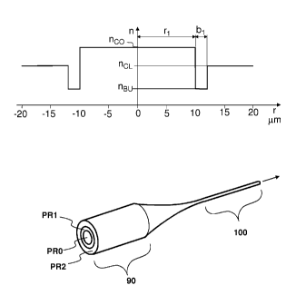
Referring to Fig. la, a light-amplifying buffered optical fiber 100
comprises a core CORI , a buffer BUF1, and a cladding CLD1. The
buffer BUF1 has an annular shape and it surrounds the core CORI .
the cladding CLD1 has also an annular shape and it surrounds the
buffer BUF1. The core CORI has a radius r1. The buffer has a radial
dimension b1. The cladding has a radial dimension cl.
The buffered fiber 100 may be a large mode area (LMA) fiber so that
the effective mode area is greater than or equal to 200 im2. The
buffered fiber 100 may be dimensioned to be a single mode fiber, or to
support only 2 - 4 transverse modes.
Referring to Fig. 1 b, the refractive index nco of the core CORI is
greater than the refractive index ncL of the cladding CLD1 in order to
confine waveguided light to the core CORI .
The refractive index ncL of the cladding CLD1 may be selected to
implement a desired numerical aperture NA of the fiber 100. A small
numerical aperture NA may facilitate suppressing the propagation of
high order modes in the fiber 100, in particular when the fiber has a
large mode area. Suppressing of the high order modes may facilitate
improving the beam quality.
The refractive index nco of the core CORI and/or the refractive index
ncL of the cladding CLD1 may be increased by doping with e.g.
germanium oxide (Ge02), phosphorus oxide (P205), and/or aluminium
oxide (A1203).
The radial dimension b1 of the buffer and the refractive index difference
nco - ncL may be selected to implement a numerical aperture NA which
is e.g. in the range of 0.05 to 0.065.
The refractive index nBu of the buffer BUF1 is lower than the refractive
indices nco and ncL. The buffer BUF1 may consist of substantially pure
amorphous silica. Thus, the refractive index nBu of the buffer BUF1
may be substantially equal to the refractive index of undoped silica.
CA 02680395 2009-09-09
WO 2008/110668 PCT/F12008/050121
8
The refractive index of silica depends on the wavelength. For ultraviolet
grade silica and full spectrum grade fused silica, the refractive index is
in the range of 1.438 to 1.551 when the wavelength is in the range of
0.2 to 2 pm.
The variation of the refractive index between core CORI , buffer BUF1
and cladding CLD1 may be step-wise or gradual. The radius r1 of the
core CORI is defined by the mid-way, i.e. the average between the
maximum refractive index of the core reg and the minimum refractive
index of the first cladding region CR1. The second radius R2 is defined
by the mid-way between the minimum refractive index of the core
region CRO and the maximum refractive index of the second cladding
region CR2.
The radius r1 of the core CORI may be e.g. substantially equal to 10
pm. The radial dimension b1 of the buffer may be e.g. substantially
equal to 2 pm. The radial dimension c1 of the cladding CLD1 may be
e.g. greater than 5 pm. The outer radius r2 of the buffer is equal to r1 +
b1.
Fig. 2a shows a radial refractive index profile of a buffered fiber 100,
which forms the basis for mode field distributions shown in Figs. 3a and
3b, as well as the basis for calculating the cut-off wavelengths shown in
Fig. 4.
Fig. 2b shows the radial refractive index profile of a reference fiber
which does not have the buffer. The reference fiber has the same core
radius r1 as the buffered fiber of Fig. 2a.
The solid curve LPO1B in Fig. 3a shows the radial mode field
distribution of the LPoi mode in the buffered fiber of Fig. 2a. The
dashed curve LPO1REF shows the radial mode field distribution of the
LPoi mode in the reference fiber of Fig. 2b.
The solid curve LP11B in Fig. 3b shows the radial mode field
distribution of the LPi 1 mode in the buffered fiber of Fig. 2a. The
CA 02680395 2009-09-09
WO 2008/110668 PCT/F12008/050121
9
dashed curve LP11REF shows the radial mode field distribution of the
LPii mode in the reference fiber of Fig. 2b.
The fields of both modes LPoi and LPi I penetrate into the buffer. Thus,
the equivalent refractive index difference between the core and the
cladding is lower in the buffered fiber than in the reference fiber. The
reduction of the equivalent refractive index difference results as a
decrease in the cut-off wavelength and as a decrease in the numerical
aperture NA.
The effective numerical aperture may be adjusted by selecting the
radial dimension b1 of the buffer, while keeping the refractive indices of
the core and the cladding constant.
The radial dimension b1 of the buffer BUF1 may be selected to
correspond to the refractive index nco of the core CORI and/or the
refractive index ncL of the cladding CLD1 in order to implement a
desired numerical aperture NA. In other words, the numerical aperture
NA may be fine-tuned by selecting the radial dimension b1 of the buffer
BUF1.
The mode field diameter is slightly smaller in the buffered fiber than in
the reference fiber.
The round and rectangular dots in Fig. 4 show calculated cut-off
wavelengths of high order modes for various fibers. lu denotes a dot
for a buffered fiber 100 wherein the radial dimension of the buffer is 1
pm and the equivalent numerical aperture NA is 0.055. 2u denotes a
dot for a buffered fiber 100 wherein the radial dimension of the buffer is
2 pm and the equivalent numerical aperture NA is 0.05. 3u denotes a
dot for a buffered fiber 100 wherein the radial dimension of the buffer is
3 pm and the equivalent numerical aperture NA is 0.05. N4 denotes a
dot for a reference fiber, i.e. without a buffer, wherein the numerical
aperture NA is 0.04. N5 denotes a dot for a reference fiber whose
numerical aperture NA is 0.05. N6 denotes a dot for reference fiber
whose numerical aperture NA is 0.06. N7 denotes a dot for a reference
fiber whose numerical aperture NA is 0.07.
CA 02680395 2014-09-29
The calculations were made in the wavelength range 800 to 1900 nm. The
calculations indicate that the presence of the buffer reduces the cut-off
wavelength.
5
The buffered fiber having the 11.1m buffer (i.e. the radial dimension of the
buffer is 1 pm) guides only two modes, whereas a corresponding
reference fiber guides 4 modes.
10 Fig. 5 shows, by way of example, a measured radial refractive index
profile for a manufactured fiber preform. A core was made by the direct
nanoparticle deposition (DND). The core was covered by a pure silica
tube, and the silica tube was subsequently covered with a germanium-
doped glass tube.
The core CORI may be doped with one or more light-amplifying dopants.
The dopant may be e.g. a rare earth metal ion. In particular, the core may
be doped with erbium, ytterbium, praseodymium or thulium. The doping
may substantially contribute to the increase of the refractive index.
Referring to Fig. 6, the material of the core CORI may be produced, for
example by the direct nanoparticle deposition (DND) method, as will be
described below. The direct nanoparticle deposition method is also
described in US20060001952 Al.
The materials of the core and/or the cladding may also be produced using
modified chemical vapor deposition (MCVD), using outside vapor
deposition (OVD), or using plasma chemical vapor deposition (PCVD).
The direct nanoparticle deposition method comprises at least the steps of:
- discharging atomizing gas 20,
- atomizing at least one first reactant 10 in liquid form by said atomizing
gas 20 to form droplets 15,
- introducing said droplets 15 into a flame 70,
CA 02680395 2009-09-09
WO 2008/110668 PCT/F12008/050121
11
- oxidizing at least one second reactant 10 in said flame 70 to form one
or more oxides,
- condensing said one or more oxides to produce particles 50,
- collecting at least a part of said particles 50 on a mandrel 80, and
- fusing said collected particles together to form light-amplifying optical
material (this step is not shown in Fig. 6).
A burner assembly 60 suitable for use in the direct nanoparticle
deposition method may comprise four tubes 11, 21, 31, 41, which
define four concentric nozzles 12, 22, 32, 42. The innermost nozzle,
herein called as the liquid nozzle, is used for delivering liquid reactant
10. The outer surface of the tube 11 and the inner surface of the tube
21 define together an annular atomizing gas nozzle 22, from which an
atomizing gas 20 is discharged. The atomizing gas is accelerated by a
pressure difference prevailing over the nozzle 22. The velocity of the
atomizing gas 20 may be further accelerated by the constriction 24 of
the nozzle 22.
There is a liquid surface 14 at the liquid nozzle 12. Shear and
aerodynamic forces generated by the stream of the atomizing gas 20
tear micrometer-sized droplets 15 from the liquid surface 14 causing
atomization. The droplets may be further fragmented by turbulence.
The droplets are entrained within the gas jet and accelerated to a high
velocity and further entrained into the flame 70.
The reactants delivered by the nozzles 12, 22, 32, 42 are mixed by
turbulence and by diffusion. Exothermic reactions of the reactants,
especially the oxidation of hydrogen provides the heat required for the
flame 70. A high temperature is achieved. The reactants 10, 20, 30
react and oxidize in the flame 70 by producing oxides and other
compounds. The saturated vapor pressures of the formed compounds
are advantageously so low that they are rapidly nucleated and
condensed forming nanometer-sized particles 50. The condensation is
further promoted by the turbulent mixing of surrounding cool gas with
the hot reaction gases, which rapidly decreases the average
temperature of the gases.
CA 02680395 2009-09-09
WO 2008/110668 PCT/F12008/050121
12
The size of the produced particles 50 may be smaller than 100 nm. The
produced doped glass particles are collected on a mandrel 80. Gas
streams G transport the particles 50 near the surface of the mandrel
80. The final transport takes place mainly by thermoforesis.
The direct nanoparticle deposition may be used to produce e.g.
erbium-doped silica. In order to produce erbium-doped silica material,
the liquid reactant delivered by the nozzle 12 is advantageously erbium
chloride and aluminum chloride dissolved in methanol. The atomizing
gas delivered by the atomizing gas nozzle 22 is hydrogen. Silicon
tetrachloride is delivered by the annular nozzle 32, and oxygen is
delivered by the annular nozzle 42. The role of aluminum chloride is to
increase the refractive index and to improve the solubility of erbium in
the produced silica glass.
The refractive index of the produced optical material may be adjusted
e.g. by changing the relative fraction of aluminum chloride in the liquid
reactant 10.
The optimum combination of the flow rates of the reactants 10, 20, 30,
40, the composition of the reactants 10, 20, 30, 40, and the dimensions
of the nozzles 12, 22, 32, 42 are optimized according to the
predetermined target properties of the light-amplifying optical material.
The preferred approach is that the optimum flow rates, compositions
and dimensions are determined by an experimental procedure known
by a person skilled in the art.
In order to achieve desired light-amplifying properties of the end-
product, the liquid reactant 10 may comprise a compound which may
comprise at least one metal selected from the groups IA, IB IIA, IIB IIIA,
IIIB, IVA, IVB, VA, and the rare earth series of the periodic table of
elements. Especially, the liquid reactant 10 may comprise erbium,
ytterbium, neodymium and/or thulium. Silica-forming compounds may
also be introduced in liquid form, for example by introducing siloxane.
In some applications, one of the reactants may be clean room air. The
atomizing gas 20 may be a premixed mixture of a combustible gas and
CA 02680395 2009-09-09
WO 2008/110668 PCT/F12008/050121
13
an oxidizing gas, especially a premixed mixture of hydrogen and
oxygen.
Light-amplifying optical waveguides made using the direct nanoparticle
deposition method have been commercially available, e.g. products
called as "Erbium doped fiber Er16-8/125", "Erbium doped fiber Er20-
4/125", and "Erbium doped fiber Er 30-4/125", supplied by a finnish
company Liekki Oy, on December 17, 2004.
A special advantage associated with the direct nanoparticle deposition
method is that a high dopant concentration may be achieved while
keeping the percentage of clustered dopant ions at a low level.
Referring to Fig. 7, the particles 50 of optical material may be
deposited on a rotating mandrel 80 to form a tubular agglomerate 88.
The mandel 80 is rotated by the rotation mechanism 66. The mandel
80 and/or the burner assembly 60 may be moved in the longitudinal
direction. The deposition system may comprise apparatus for
monitoring the thickness of the tubular agglomerate 88 and for
controlling the chemical composition of the produced material as a
function of said thickness.
After the deposition step, the tubular agglomerate 88 may be removed
from the mandrel 80. The tubular agglomerate 88 may be subsequently
inserted into a furnace (not shown) for purification and sintering, using
methods known by the person skilled in the art. Subsequently, the
agglomerate 88 may be collapsed to form a rod 91 (see Fig. 8) of
doped silica glass, using methods known by the person skilled in the
art.
A preform 90 for manufacturing a buffered fiber 100 may comprise:
- a rod 91 having a refractive index nco,
- a first glass tube having a refractive index nBu which is substantially
equal to the refractive index of pure amorphous silica, and
- a second glass tube having a refractive index ncL which is higher than
nBU=
CA 02680395 2009-09-09
WO 2008/110668 PCT/F12008/050121
14
Referring to Fig. 8, the rod 91 is combined with a first glass tube 92
and a second glass tube 93 to form a fiber preform 90 (see Fig. 9). The
rod 91 and the tubes are positioned inside each other and fused
together using so-called sleeving techniques known by the person
skilled in the art. The refractive index of the first tube 92 is equal to the
refractive index of pure silica glass. The refractive index of the second
tube 93 is greater than the refractive index of the first tube 92.
Referring to Fig. 9, the fiber preform 90 is heated and drawn to form
the light-amplifying optical fiber 100, using methods known by the
person skilled in the art. The form of the radial refractive index profile is
substantially preserved in the drawing process. Thus, the fiber 100
having the predetermined refractive index profile may be drawn from
the preform 90 which has a profile of the same form. The core region
PRO of the preform 90 consists of the material of the rod 91 (Fig. 8).
The buffer region PR1 of the preform 90 consists of the material of the
first tube 92. The cladding region PR2 of the preform 90 consists of the
material of the second tube 93. The core CORI of the fiber 100 consists
of the material of the core region PRO of the preform 90. The material
of the buffer BUF1 of the fiber 100 consists of the material of the first
cladding region PR1 of the preform 90. The material of the cladding
CLD1 of the fiber 100 consists of the material of the second cladding
region P R2 of the preform 90.
Referring back to Fig. 7, the glass materials corresponding to the buffer
BUF1 and to the cladding CLD1 may also be deposited directly over
the agglomerate 88. The thickness of the collected deposit may be
monitored and the composition of the produced particles 50 may be
changed during the deposition process such that the agglomerate will
have a refractive index profile which corresponds to the predetermined
refractive index profile of the fiber 100.
Thus, a method for producing the preform 90 of an optical waveguide
100 may comprise:
-providing a rod 91,
- coating said rod 91 with a first glass layer 92 such that said first glass
layer 92 surrounds said rod 91, and
CA 02680395 2009-09-09
WO 2008/110668 PCT/F12008/050121
- coating said first glass layer 92 with a second glass layer 93 such that
said second glass layer 93 surrounds said first glass layer 92.
The rod 91, the first glass layer 92, and the second glass layer 93 may
5 comprise silica glass. The refractive index of the first glass layer 92
may be substantially equal to the refractive index of pure amorphous
silica glass. In particular, the first glass layer 92 may consist of pure
silica glass. The material of the rod 91 may be doped with at least one
light-amplifying dopant.
The first glass layer 92 may be produced directly on the rod 91 (i.e. on
an agglomerate 88) by using the direct nanoparticle deposition.
Sintering and collapsing of the preform 90 may be performed after the
first glass layer 92 has been deposited on the rod 91.
A free-standing heated rod 91 may be deformed when heated. For
example the cross-section of the rod 91 may be deformed from a
substantially circular shape to an elliptical shape.
Deformation of the geometrical shape of the rod 91 during sintering
and/or collapsing may be substantially reduced if the first glass layer 92
has been deposited on the rod 91 (agglomerate 88) before sintering
and collapsing. The first layer 92 of substantially pure silica glass has
typically a higher glass transition temperature ("softening point") than
the doped material of the rod 91. Thus, the heated combination of the
rod 91 and the first glass layer 92 is typically more rigid than a free-
standing rod 91 which has been heated to the same temperature.
The second glass layer 93 may be provided e.g. by fusing a glass tube
93 to the first layer 92 such that the glass tube 93 surrounds the first
layer 92. Alternatively, the second glass layer 93 may be provided e.g.
by direct nanoparticle deposition (DND).
The fiber 100 according to the present invention may comprise further
layers (not shown) surrounding the cladding CLD1 to provide e.g.
mechanical and chemical protection, strain relief, and/or blocking of
stray light.
CA 02680395 2009-09-09
WO 2008/110668 PCT/F12008/050121
16
The cladding CLD1 may be further doped with substances, e.g. Ti02,
P205 or B203, which makes the fusing of the fiber to another silica-
based fiber easier.
The fiber 100 may be used to implement e.g. an optical amplifier.
The fiber 100 may be optimized to achieve low bending losses, i.e. to
minimize the loss of light in bent sections of the fiber 100.
The fiber 100 may be designed to provide a low dispersion over a wide
and predetermined wavelength range.
The fiber 100 may be a dispersion-shifted fiber, i.e. it may be designed
to provide a zero-dispersion property at a predetermined wavelength,
which predetermined wavelength is shifted with respect to the zero-
dispersion wavelength of a reference fiber without the buffer.
The fiber 100 according to the present invention may be designed to
act as a short-pass filter, i.e. to attenuate light which has a wavelength
greater than a predetermined value.
The radius r1 of the core of the waveguide 100 may be greater than or
equal to 3 pm.
The ratio of the radial dimension b1 of the buffer BUF1 to the radius r1
of the core CORI may be e.g. in the range of 0.05 to 0.4.
The numerical aperture of the waveguide 100 may be tuned by
adjusting the radial dimension of the buffer BUF1 so as to attain a
predetermined numerical aperture.
Said adjustment may be performed according to the refractive index
nco of the core CORI and according to the refractive index ncL of the
cladding CLD1.
CA 02680395 2009-09-09
WO 2008/110668 PCT/F12008/050121
17
The difference between the predetermined numerical aperture and the
attained numerical aperture may be e.g. smaller than or equal to 0.005,
preferably smaller than or equal to 0.002.
Variations in the refractive indices nco and ncL may be compensated by
adjusting the radial dimension b1 of the buffer BUF1.
Multimode fibers having a large mode area (LMA) have a relatively low
numerical aperture. The numerical aperture of the optical waveguide
100 may be e.g. in the range of 0.05 to 0.08. Implementation of such a
low numerical aperture typically requires accurate control of the
refractive index of the core CORI and the cladding CLD1. Thanks to
the invention, larger variations in the refractive indices may now be
allowed. The effect of the variations in the refractive indices on the
numerical aperture may be compensated by adjusting the radial
dimension B1 of the buffer BUF1. Consequently, the manufacturing
yield may be increased.
For example, a waveguide 100 having a numerical aperture of 0.070
may be manufactured (without the buffer) by using a core material
which has a refractive index 1.4620 and cladding material which has a
refractive index of 1.4603. If the refractive index of the doped core
material would be e.g. 1.4615, the corresponding numerical aperture
would be 0.060 (without buffer). Thus, the deviation of 0.0005 in the
refractive index of the core may be sufficient to cause a deviation of
0.010 between the attained numerical value 0.060 and the
predetermined numerical aperture 0.070. The difference 0.010
corresponds to 14% deviation when compared with the predetermined
target value 0.070. This deviation may be compensated by adjusting
the radial dimension B1 of the buffer BUF1 in order to attain the
predetermined numerical aperture 0.070.
The numerical aperture of the waveguide 100 may be tuned by
adjusting the radial dimension of the buffer BUF1 when the refractive
index nBu of the buffer BUF1 is smaller than the refractive index ncL of
the cladding CLD1. In particular, the numerical aperture of the
waveguide 100 may be tuned by adjusting the radial dimension of the
CA 02680395 2009-09-09
WO 2008/110668 PCT/F12008/050121
18
buffer BUF1 when the refractive index nBu of the buffer BUF1 is smaller
than the refractive index ncL of pure amorphous silica, i.e. when the
also buffer BUF1 has been doped.
However, precise controlling of the refractive index is more difficult if
the refractive index of the buffer BUF1 has been modified by doping,
when compared with a situation when the refractive index of the buffer
BUF1 is substantially equal to the refractive index of pure amorphous
silica.
Furthermore, embodiments with pure silica buffer are less susceptible
to bubble formation than embodiments with a doped buffer.
The waveguide 100 may be drawn from the preform 90. The ratio of
the radial dimension of the first glass tube 92 to the radius of the rod 91
may be selected according to the refractive index nco of the rod and
the refractive index ncL of the second glass tube already when making
the preform 90. Said ratio may be selected such that a predetermined
numerical aperture and/or a predetermined cut-off wavelength kc of
single mode operation may be attained when a waveguide 100 having
a predetermined core radius r1 is drawn from said preform 90.
The waveguide 100 may be drawn from the preform 90. The ratio of
the radial dimension of the first glass layer 92 to the radius of the rod
91 (agglomerate 88) may be selected according to the refractive index
nco of the rod and the refractive index ncL of the second glass layer
already when making the preform 90. Said ratio may be selected such
that a predetermined numerical aperture and/or a predetermined cut-off
wavelength kc of single mode operation may be attained when a
waveguide 100 having a predetermined core radius r1 is drawn from
said preform 90.
The refractive indices, the numerical aperture, and the mode area may
be determined at a predetermined wavelength of light, e.g. at k=1000
nm (in vacuum).
CA 02680395 2009-09-09
WO 2008/110668 PCT/F12008/050121
19
An increase of the radial dimension b1 of the buffer BUF1 may
decrease the cut-off wavelength kc of the waveguide 100 (see Fig. 4).
An equivalent numerical aperture NAeg of the waveguide 100 may be
calculated from the cut-off wavelength kc by using equation (1):
NA ¨ 2.405Ar
(1)
eq 27171
where NAeg denotes effective numerical aperture, kc denotes cut-off
wavelength (in vacuum), and r1 denotes the radius of the core CORI .
kc is the cut-off wavelength for single mode operation, i.e. only single
mode operation is possible when the wavelength is shorter than or
equal to the cut-off wavelength kc.
The tails of mode field distributions of the higher order modes may
extend through the buffer BUF1 deeper into the cladding CLD1 than
the tail of mode field distribution of the LPoi mode (see Figs. 3a and
3b). This effect may be controlled by adjusting the radial dimension b1
of the buffer BUF1. It may even be so that the tail of the LPoi mode
does not penetrate through the buffer BUF1 although the tails of the
mode field distributions of the higher order modes penetrate through
the buffer BUF1. Thus, the tails of the mode field distributions of the
higher order modes may interact with a lower refractive index
difference than the tail of the LPoi mode. Consequently, for
wavelengths shorter than or equal to kc, the LPoi mode may still be
confined to the waveguide 100 while the higher order modes are not
supported by waveguide 100.
The maximum radial dimension b1 of the buffer BUF1 may be limited
e.g. to the maximum distance of mode penetration from the boundary
of the core CORI . The tail of the mode field of the LPoi mode may be
considered to extend up to a penetration radius where 10-10 of the
energy of the LPoi mode is carried outside said penetration radius. The
maximum radial dimension b1 of the buffer BUF1 may be limited so
that the buffer does not extend beyond said penetration radius. The
maximum radial dimension b1 of the buffer BUF1 may be e.g. 5 pm.
CA 02680395 2009-09-09
WO 2008/110668 PCT/F12008/050121
A predetermined cut-off wavelength kc may be implemented for the
waveguide 100 by selecting the radial dimension b1 of the buffer BUF1
according to the refractive index nco of the core CORI and the
refractive index ncL of the cladding CLD1. In other words, the radial
5 dimension b1 of the buffer BUF1 may be adjusted so as to tune the
cut-off wavelength A.c of said optical waveguide 100 to a predetermined
target value
It may be deduced from eq. (1) that an increase of the radial dimension
10 b1 of the buffer BUF1 may decrease the equivalent numerical aperture
NAeg of the waveguide 100.
The equivalent numerical aperture NAeg of the waveguide 100 may be
adjusted by adjusting the radial dimension b1 of the buffer BUF1. Thus,
15 a method for producing an optical waveguide may comprise adjusting
the radial dimension b1 of the buffer BUF1 so as to attain a
predetermined equivalent numerical aperture NAeg of said optical
waveguide 100.
20 The radial dimension b1 of the buffer BUF1 may be adjusted e.g. by
selecting the ratio of the radial dimension b1 to the radius r1 of the core
CORI of the waveguide 100 in the preform or deposition stage, and
drawing the waveguide 100 from the preform so as to attain a
predetermined core radius r1.
The radial dimension b1 may also be fine-tuned in the fiber drawing
phase by allowing small variations in the total diameter of the drawn
waveguide 100.
For a person skilled in the art, it will be clear that modifications and
variations of the fiber according to the present invention, the fiber
preform according to the present invention, the method of
manufacturing said fiber and the method of manufacturing said preform
are perceivable. The particular embodiments described above with
reference to the accompanying drawings are illustrative only and not
meant to limit the scope of the invention.