Note: Descriptions are shown in the official language in which they were submitted.
CA 02681173 2013-01-30
PIEZOELECTRIC VIBRATIONAL ENERGY HARVESTING SYSTEMS
INCORPORATING
PARAMETRIC BENDING MODE ENERGY HARVESTING
FIELD OF THE INVENTION
[0001] The present invention generally relates to the field of vibrational
energy
scavenging. In particular, the present invention is directed to piezoelectric
vibrational energy
harvesting systems incorporating parametric bending mode energy harvesting.
BACKGROUND
[0002] Over the last quarter-century there has been a drastic increase in the
level of
integration of integrated circuits (ICs). At the same time, there has been a
corresponding
significant decrease in the feature size of ICs. For example, the width of a
MOSFET (metal-
oxide-semiconductor field-effect transistor) gate is presently on the order of
45 nm and is
projected to be 18 nm in 2010. This is less than 1/500 the width of a human
hair. IC
components have not only dramatically reduced in size, but have also reduced
in power
consumption. ICs are typically made using CMOS (complementary metal-oxide
semiconductor) circuitry, which is made of dual n-FET and p-FET devices. CMOS
circuitry
consumes much less power than either purely nMOS or purely pMOS circuitry.
[0003] Reduction in both size and power consumption of ICs has led to the
recent
proliferation of wireless IC technology, which was not available just a decade
ago. Today,
there is a diversity of devices using low-power wireless circuits, including
laptop computers,
cell phones, MP3 players, smart phones, telephony headsets, headphones,
routers, gaming
controllers, mobile Internet adaptors, and spy cameras, to name just a few. Of
course, each of
these devices requires some sort of standalone power supply to work. Typically
power
supplies for these devices are electrical batteries, often replaceable
batteries.
[0004] A wireless technology field of significant current interest, and that
is the target for
1
4182119 v2
CA 02681173 2013-01-30
much research, is the field of wireless sensor networks. Indeed, researchers
envision the
future to include a widespread adoption of wireless sensor networks (WSNs). In
WSNs,
wireless sensors will be distributed throughout a particular environment to
form an ad-hoc
network or mesh that relays measurement data to a central hub. The particular
environment
could be any one of an automobile, an aircraft, a factory, and a building,
among many others.
A WSN will comprise several to tens of thousands wireless sensor nodes that
will operate
using multi-hop transmissions over short distances. Each wireless node will
generally include
a sensor, wireless electronics and a power source. The result will be the
creation of an
intelligent environment responding to its conditions and inhabitants, if any.
[0005] A wireless sensor node, like the other wireless devices mentioned
above, needs
some sort of standalone electrical power supply to provide power to the
electronics aboard
that node. Conventional batteries, such as lithium-ion batteries, zinc-air
batteries, lithium
batteries, alkaline batteries, nickel-metal-hydride batteries and nickel-
cadmium batteries,
could be used. However, for wireless sensor nodes designed to function beyond
the typical
lifetime of such batteries, at some point the batteries would have to be
replaced. This could
cause significant problems and expense depending on the number of nodes at
issue and the
accessibility of those nodes, not to mention the need to dispose of the
batteries.
Consequently, alternatives to batteries and other types of power supplies
needing periodic
attention, such as micro-size fuel cells, will be desirable for many WSNs.
[0006] Such alternative standalone power supplies would typically rely on
scavenging (or
"harvesting") of energy from the ambient environment of a wireless sensor
node. For
example, if the wireless sensor node is exposed to sufficient light, the
alternative standalone
power supply could include photoelectric or solar cells. Alternatively, if the
wireless sensor
node is exposed to sufficient air movement, the alternative power supply could
include a
micro-turbine for harvesting power from the moving air. Other alternative
standalone power
supplies could also be based on temperature fluctuations, pressure
fluctuations or other
environmental influences.
[0007] However, there will be many instances when the ambient environment
does not
include sufficient amounts of light, air movement, temperature fluctuation and
pressure
2
4182119 v2
CA 02681173 2013-01-30
variation to provide enough power to power a particular wireless sensor node.
However, the
sensor node may be subjected to fairly predictable and/or constant vibrations,
for example,
emanating from the structure supporting the node or to which the node is
attached. In this
case, a vibrational energy scavenger (or harvester) that essentially converts
vibrational
energy into electrical energy can be used.
[0008] A particular type of vibrational energy harvester utilizes resonant
beams that
incorporate a piezoelectric material that generates electrical charge when
strained during
resonance of the beams caused by ambient vibrations (driving forces). One
shortcoming of
many conventional piezoelectric vibrational energy harvesters (PVEHs) is that
they are
minimally dampened devices having high quality factors (Q). Thus, they are
effective over
only very small bandwidths of vibrational frequency. This becomes problematic
under any
one or more of a variety of circumstances, such as when the wireless sensor
node is subjected
to temperature variations that change the tuning of the PVEH, when the
frequency of the
ambient vibrations varies over time and when the manufacturing methods used to
make the
PVEH cause variation in the as-built tuning of the PVEH.
SUMMARY OF THE DISCLOSURE
[0009] One implementation of the present invention is a vibrational energy
harvester. The
vibration energy harvester includes: a resonator beam having transverse cross-
sectional
properties, a fundamental resonance frequency in a first bending direction and
a parametric
mode frequency in a second bending direction perpendicular to said first
bending direction,
wherein said cross-sectional properties are selected to tune said fundamental
resonance
frequency to a first desired frequency and to tune said parametric mode
frequency to a
second desired frequency, said resonant beam including piezoelectric material
for generating
electrical energy in response to bending of said resonator beam in each of
said first and
second bending directions.
[0010] Another implementation of the present invention is a vibrational energy
harvesting
unit. The vibrational energy harvesting unit includes: a plurality of
piezoelectric vibrational
energy harvesting (PVEH) modules electrically connected with one another,
wherein each of
3
4182119 v2
CA 02681173 2013-01-30
said PVEH modules includes a plurality of parametric mode enabled PVEH beams
each
configured to harvest electrical charge from each of fundamental resonance
excitation and
parametric mode excitation.
[0011] Yet another implementation of the present invention is a wireless
sensor. The
wireless sensor includes: a transducer for collecting data; a wireless
transmitter for
transmitting the data to a receiver spaced from the wireless sensor; and a
parametric mode
enabled (PME) piezoelectric vibrational energy harvesting (PVEH) power supply
electrically
communicating with each of said transducer and said wireless sensor, said PME
PVEH
power supply configured to scavenge vibrational energy in an environment
ambient to the
wireless sensor when in use so as to generate electrical power for use in
powering said
transducer and said wireless transmitter during use.
BRIEF DESCRIPTION OF THE DRAWINGS
[00121 For the purpose of illustrating the invention, the drawings show
aspects of one or
more embodiments of the invention. However, it should be understood that the
present
invention is not limited to the precise arrangements and instrumentalities
shown in the
drawings, wherein:
FIG. 1 is an isometric view of an example of a piezoelectric vibrational
energy harvesting
(PVEH) unit made in accordance with concepts of the present disclosure;
FIG. 2A is an enlarged plan view of one of the PVEH modules of the system of
FIG. 1
showing multiple groups of parametric-mode-enabled (PME) PVEH beams; FIG. 2B
is an
enlarged partial cross-sectional exploded view of three of the PVEH modules of
FIG. 1
illustrating their configurations just prior to attachment to one another;
FIG. 2C is an
enlarged partial cross-sectional view of the upper six PVEH modules of FIG. 1
affixed to one
another in the finished stack;
FIG. 3 is a graph of a typical frequency spectrum (voltage versus frequency)
for a cantilever-
type PVEH beam made using conventional practices;
4
4182119 v2
CA 02681173 2013-01-30
FIG. 4 is a graph of frequency spectra (voltage versus frequency) for a set of
cantilever-type
PME PVEH beams made using concepts of the present disclosure, the graph
showing the
effects of differing width:thickness ratios on the frequency spectra of the
differing beams;
FIG. 5 is a graph of a frequency spectrum (voltage versus frequency) for a
PVEH module
containing three groups of PME beams in which the groups are tuned to slightly
different
frequencies;
FIG. 6 is an enlarged longitudinal cross-sectional view of a bimorph PME PVEH
beam made
in accordance with concepts of the present disclosure;
FIG. 7 is a cross-sectional view as taken along line 7-7 of FIG. 6;
FIG. 8 is a transverse cross-sectional view of a monomorph PME PVEH beam made
in
accordance with concepts of the present disclosure;
FIGS. 9A-P are a series of diagrams illustrating steps of a fabrication
process that can be
used to make a monomorph PME PVEH beam, wherein each of FIGS. 9A-P contains a
longitudinal cross-sectional view and a transverse cross-sectional view
relative to the
finished beam;
FIGS. 10A-I3 are a series of diagrams illustrating alternative steps that can
be used to make a
monomorph PME PVEH beam, wherein each of FIGS. 10A-B contains a longitudinal
cross-
sectional view and a transverse cross-sectional view relative to the finished
beam;
FIG. 11 is a schematic/diagrammatic view of a wireless sensor made in
accordance with
concepts of the present disclosure; and
FIG. 12 is a block diagram of a network of wireless sensors each utilizing a
PME-based
power source for powering each onboard sensor and communications within the
network.
DETAILED DESCRIPTION
[0013] Referring now to the drawings, FIG. 1 illustrates an example of a
piezoelectric
vibrational energy harvester (PVEH) unit 100 made in accordance with concepts
of the
present disclosure. As those skilled in the art will appreciate, such a PVEH
unit may be used
4182119 v2
CA 02681173 2013-01-30
to generate electrical power from scavenged vibrational energy in the ambient
environment
in which the PVEH unit is mounted or otherwise placed. Although the
illustrated PVEH unit
100 of FIG. 1 is in the microscale size regime¨this particular example is
roughly a
rectangular parallelepiped of about 7.5 mm along each base edge and 13.5 mm
along the
height¨other PVEH units made in accordance with concepts of the present
disclosure can be
alternatively constructed in another size regime, such as a mesoscale-size
regime, using
fabrication techniques that will be readily understood by those skilled in the
art. Because of
the size of exemplary PVEH unit 100, those skilled in the art will recognize
that it can be
made using MEMS (micro-electromechanical systems) fabrication techniques.
Examples of
MEMS fabrication techniques are described below in connection with FIGS. 9A-P
and 10A-
B.
[0014] PVEH units made in accordance with concepts of the present
disclosure, such as
PVEH unit 100, are particularly, though not exclusively, suited to
applications wherein the
devices they are used to power are either required or desired to be self-
contained for any one
or more of a variety of reasons, such as physical inaccessibility,
impracticability of providing
power wires or changing batteries, unavailability of alternative power sources
and cost,
among others. It is impractical to list all of the applications that can
benefit from
implementing broad concepts of the present disclosure. However, since wireless
sensor
networks are presently an important target application for this technology,
the present
disclosure contains examples of implementing these concepts in a wireless
sensor and in a
sensor network containing such a wireless sensor. That said, those skilled in
the art will
readily appreciate that wireless sensor networks are by no means the only
possible
application for the broad concepts disclosed herein.
[0015] With continuing reference to FIG. 1, and also to FIG. 2A, at a high
level, PVEH
unit 100 of this example includes sixteen PVEH modules 104A-P (one of which,
module
104C, is shown in detail in FIG. 2A). Modules 104A-P share the same general
construction,
which includes a plurality of groups of like PVEH beams, wherein all of the
beams with a
group are tuned the same and the tuning of the beams differs among the groups.
This is
illustrated in FIG. 2A by module 104C having six groups 200A-F each containing
eight
identically tuned PVEH beams 204A-F (in this example cantilever-type beams)
and in which
6
4182119 v2
CA 02681173 2013-01-30
the beam tunings differ among the six groups. In this example, the differing
tunings are
provided by changing the active lengths LA through LF of PVEH beams 204A-F,
respectively, as seen in FIG. 2A. Examples of additional/alternative ways to
vary the tunings
of PVEH beams 204A-F are mentioned below. It is also noted that in this
example each PME
PVEH beam 204A-F is a "bimorph" beam in terms of the layering of a
piezoelectric material
used to fabricate the beams and is also a "split-electrode" beam in terms of
the way the
electrodes for harvesting electrical energy from the piezoelectric material
are specially
configured for harvesting energy from the parametric mode excitation of the
beam. Each of
the bimorph and split-electrode concepts is described below in detail.
[0016] As will be appreciated by those skilled in the art, PVEH module 104C
shown in
FIG. 2A is merely one example of a virtually infinite number of configurations
of a PVEH
module that can be constructed using the broad concepts disclosed herein.
Following are a
few of the items that can be changed, alone and in various combinations with
each other, to
provide different designs: 1) the number of PVEH beams in each group may
differ from the
eight shown in different designs; 2) the number of PVEH beams can be varied
among the
groups; 3) the number of groups may differ from the six shown; 4) the number
of non-
identical groups may be different from the six shown; 5) each module may have
two or more
groups that are identical to one another; and 6) the PVEH beams may be other
than of the
cantilever type, such as the dual fixed-end type, the dual clamped-end type,
simply supported
type and mixed type that are combinations of other types, among others. The
support
conditions do not limit that application of the broad concepts of the present
disclosure.
[0017] Furthermore, all of PVEH modules 104A-P need not be the same as module
104C
shown in FIG. 2. For example, if six differing beam tunings are desired, all
sixteen PVEH
modules 104A-P of FIG. 1 may be identical. However, six differing beam tunings
can be
provided in other ways. For example, each PVEH module may provide two
differing tunings,
such that at least two others of the modules each provide yet two different
tunings. As
another example, entire PVEH modules may have only one beam tuning, so that
the six
different tunings are provided by at least six modules all having tunings
differing from one
another. The foregoing is just a sample of many variations that can be made to
achieve a
desired goal.
7
4182119 v2
CA 02681173 2013-01-30
[0018] It is also noted that a PVEH unit made using broad concepts disclosed
herein can
vary in the number of differing beam tunings according to the particular
design parameters at
issue. For example, in some applications, only a single beam tuning will be
needed for an
entire PVEH unit, whereas for other applications, three, six, ten or more
differing tunings
may be beneficial. Some factors involved with determining how many beam
tunings should
be provided are discussed below.
[0019] A PVEH unit made in accordance with concepts of the present disclosure,
such as
PVEH unit 100 of FIG. 1, will include any one or more of a number of features
that can give
it a relatively high power density (power generated per unit volume) and can
provide it with
a relatively wide frequency response. These features include specially
designed PVEH beams
that not only harvest vibrational energy from fundamental-mode excitation of
the beams in
the direction of the driving vibration, but also harvest energy from
parametric-mode
excitation of the beams. Parametric-mode excitation is a non-linear resonance
mode
perpendicular to the driving force (vibration). The PVEH beams of the present
disclosure that
are specially designed to harvest energy from parametric-mode excitation are
conveniently
referred to herein and in the appended claims as "parametric mode enabled," or
"PME." By
varying the cross-sectional properties of each PME beam, the frequency of
parametric-mode
excitation of that beam is tunable to create the desired effect of either
increasing the power
density of a PVEH unit or increasing the effective excitation bandwidth of the
unit, or both.
In addition to increasing the effective excitation bandwidth of each beam by
tuning the
parametric-mode excitation frequency, the overall excitation bandwidth of a
PVEH unit of
the present disclosure can be increased by providing multiple groups of PVEH
beams
wherein the groups are tuned to slightly different frequencies. This is
illustrated in the
context of module 104C of FIG. 2A by the presence of the six groups 200A-F
having six
different tunings, as illustrated visually by the six different lengths LA
through LF of beams
204A-F, respectively. As described below, the differing tunings can be
provided in other
ways, such as providing beams 204A-F in differing groups with differing proof
masses (228
in FIGS. 2B and 2C) and a combination of varying the lengths LA through LF and
providing
differing proof masses, among others.
8
4182119 v2
CA 02681173 2013-01-30
100201 Before describing several examples of PME PVEH beams, it is seen in
FIG. 1 that
PVEH modules 104A-P are configured stacked and secured with one another and
with end
modules 108A-B so as to form an integrated, self-packaged unit. Although not
illustrated in
detail in FIG. 1, PVEH modules 104A-P are electrically connected with one
another and with
end modules 108A-B so that the electrical power available from outputs 112,
116 is the sum
of power generated by all of the PME PVEH beams, such as beams 204A-F (FIG.
2A), of all
of the PVEH modules. As those skilled in the art will understand, PME modules
can be
electrically connected to one another in either series or parallel, depending
on the particular
deployment of PVEH unit 100. In this example, which again is in the microscale
regime,
each PVEH module 104A-P is a silicon-based die made using various layer
deposition,
removal and etching techniques. Several processing techniques suitable for use
in making
such modules are described below in connection with FIGS. 9A-P and FIGS. 10A-
B. End
modules 108A-B of this example are also made using similar techniques, and the
various
PVEH modules 104A-P and end modules are bonded to one another using suitable
bonding
techniques. An example of a suitable bonding technique is described below in
connection
with FIGS. 2B-C. It is noted that one or both end modules 108A-B may include
rectifying
and regulating circuitry (not shown) as appropriate for a particular design.
100211 FIGS. 2B-C illustrate an example of how the PVEH modules 104A-B and end
modules 108A-B of FIG. 1 may be secured and electrically connected to one
another. FIG.
2B illustrates three of PVEH modules 104A-P of FIG. 1, specifically PVEH
modules 104E-
G, in proper relation to one another as they would be during formation of the
stack of PVEH
unit 100 (FIG. 1). As seen in FIG. 2B, in this example, each module 104E-G is
provided with
glass fit 208 that will be used to bond the modules to each other in a vacuum
assembly
process. Glass frit 208 is placed in a manner that will hermetically seal the
cavities 212 that
will contain the beams (here, beams 204A) after PVEH modules 104E-G are
secured to one
another. A ball of solder 216 is placed on each PVEH module 104E-G at each
location where
electrical connection must be made between the modules. In this design, the
bottom electrode
220 is electrically connected to the silicon substrate 224. FIG. 2C shows the
upper six
modules, i.e., end module 108A and PVEH modules 104A-E, bonded to one another
after the
vacuum assembly process. As can be seen in FIG. 2C, during the vacuum assembly
process
9
4182119 v2
CA 02681173 2013-01-30
that includes heating modules 104A-E, 108A to a sufficient temperature that
melts glass fit
208 and solder balls 216, the solder balls flow and solidify to form fill a
space between
adjacent modules, thereby providing electrical continuity between the adjacent
modules.
During the vacuum assembly process, a vacuum is formed in each of cavities
212, and that
vacuum is held by the hermetic seal provided by the melted and solidified
glass frit 208.
[0022] For the sake of illustration, the following Table provides
approximate minimum
and maximum values of a number of relevant parameters for a set of exemplary
microscale
PVEH units (not shown) generally similar to PVEH unit 100 of FIG. 1. Like PVEH
unit 100,
each of the individual PVEH modules in the exemplary set (corresponding to
ones of PVEH
modules 104A-P) is a 7.5 mm x 7.5 mm square die having a thickness of 675 p.m,
which is a
typical thickness of a 150 mm diameter silicon wafer. Of course, other wafer
thicknesses can
be used, but a 675 JAM thick wafer provides ample thickness for creating the
two-sided
cavities 212 illustrated in FIGS. 2B-C. The end modules (corresponding to end
modules
108A-B of FIG. 1) in this example are made from the same wafer(s) as used to
make the
PVEH modules and, therefore, have the same thickness. Each of the dies
corresponding to
the PVEH modules includes bimorph, split-electrode PME PVEH beams made using
the
processing techniques described below in connection with FIGS. 9A¨P and 10A-B.
In this
example, each PVEH module (chip) contained eight like-tuned groups each having
twelve
PME PVEH beams electrically connected together in series and produces 0.2 V
and 100 m
of power. In this example, all of the PVEH beams in each PVEH module are
electrically
connected in series so as to maximize the voltage across the respective output
nodes.
Consequently, 10 dice stacked electrically in series, after rectification
(assume a 0.5 V loss),
will achieve 1.5 V and 1 mW of power. This will be a 7.425 mm tall stack,
including a cap
chip. Similarly, a 4.05 mm tall stack will produce 0.5 V and 0.5 mW of power,
a 10.8 mm
stack will produce 2.5 V and 1.5 mW of power, a 20.925 mm high stack will
produce 5.5 V
and 3 mW of power, etc.
[0023] Of course, the values in the following table are specific to this
example and similar
values for other PVEH units made in accordance with the broad concepts
disclosed herein
will have other values depending on their scale and construction. For example,
while
minimum and maximum operating frequencies in the Table are indicated as 50 Hz
and 1500
4182119 v2
CA 02681173 2013-01-30
Hz, respectively, PVEH units and modules made in accordance with the broad
principles
disclosed herein can be made to have other operating frequencies. That said
and generally
speaking, many applications for PVEH units and modules made in accordance with
the
present disclosure will likely require operating frequencies (bands) in a
range of 50 Hz to 250
Hz.
TABLE
Parameter Min. Max. units
Volume 0.22 1.17 cm3
Voltage 0.5 5.5 Volts
Power 0.5 3.0 mWatts
Power Density 2.27 2.72 mW/cm3
Acceleration lg lg ¨
Frequency 50 1500 Hertz
Bandwidth 2 10 Hertz
Note: All values estimated
[0024] FIGS. 3-5 are presented to highlight differences between PME PVEH
technology
of the present disclosure and conventional PVEH technology, as well as to
explain concepts
attendant the exploitation of parametric mode excitation. FIG. 3 is a
frequency spectrum 300
for a conventional rectangular-cross-sectioned cantilever PVEH beam having a
width that is
much greater than its thickness. For example, the width of such a conventional
PVEH beam
would be on the order of 50 times the thickness of the beam. FIG. 3 also shows
schematically
a cantilever beam 304 and the coordinate system 308 used in connection with
FIGS. 3-5 (and
also FIGS. 6-8). In a conventional PVEH beam having a width much greater than
its
thickness, parametric mode excitation is essentially nonexistent.
Consequently, and
considering only the first harmonic, frequency spectrum 300 has only a
fundamental
resonance frequency peak 300A, here at 120 Hz 2Hz, due to first bending mode
excitation
11
4182119 v2
CA 02681173 2013-01-30
in the ZX-plane and a first harmonic frequency peak 300B, here at 751.2 Hz
2Hz, due to
second mode excitation also in the ZX plane, each due to a driving vibration
in the ZX-plane.
[00251 FIG. 4 reproduces frequency spectrum 300 of FIG. 3, and its fundamental
and first
harmonic peaks 300A-B, respectively and also contains six additional peaks
400, 402, 404,
406, 408, 410 resulting from beam bending in the YZ plane due to parametric
mode
excitation at differing width: thickness ratios much smaller than the ratio
(>50) of FIG. 3.
Again, the parametric mode excitation causes bending in a plane, here the YX-
plane)
perpendicular to the plane of driving vibration, here the ZX-plane. It is
noted that frequency
spectrum 300 is equally applicable to the much narrower beams that provide
parametric-
mode peaks 400, 402, 404, 406, 408, 410 because, generally, for a beam of a
particular Z-
direction thickness the frequency response spectrum does not change with
changing Y-
direction widths.
100261 As seen from FIG. 4, parametric-mode peaks 400, 402, 404, 406,
408, 410
correspond, respectively, to width:thickness ratios of 1.5, 2, 3, 4, 5 and 7,
with the heights of
these peaks decreasing as the ratio increases. While any of these, or other
similarly valued
width:thickness ratios, can be exploited for parametric mode vibrational
energy harvesting,
ratios of 1 to around 1.5 are of particular note since the corresponding
response peaks
(illustrated by peak 400) in this range overlap with fundamental resonance
peak 300A.
Generally, a width:thickness ratio puts the frequency of the parametric mode
excitation
within about 5 Hz of the fundamental resonance frequency. Consequently,
implementing
width:thickness ratios in this regime in conjunction with circuitry that
exploits the attendant
parametric mode excitation can be used to broaden the useful bandwidth of a
PVEH device,
such as PVEH unit 100 of FIG. 1. It is noted that at a width:thickness ratio
of 1, the
parametric mode peak (not shown) would coincide with fundamental resonance
peak 300A.
Consequently, use of appropriate circuitry that fully exploits both
fundamental resonance
excitation and parametric mode excitation could essentially double the output
of a PME
PVEH device relative to the same device that exploits only the fundamental
resonance
excitation.
12
4182119 v2
CA 02681173 2013-01-30
100271 While tuning a PME PVEH beam so that the parametric mode excitation
frequency
is close to the fundamental resonance frequency of the beam is very useful in
broadening the
bandwidth of the frequency response of that beam, those skilled in the art
will readily
appreciate that other parametric mode tunings may also be useful. Generally,
but without
necessarily being limiting, it is presently envisioned that tunings (for
rectangular cross-
sectioned beams) that may find useful application vary from a width:thickness
ratio of 1:1 to
8:1. For example, there may be environments containing two specific fixed
vibration
frequencies that are more than 5 Hz apart (width:thickness ratio > 1.5). In
such a case, the
fundamental resonance frequency of a PME PVEH beam could be tuned to one of
the
frequencies and the parametric mode frequency could be tuned to the other,
say, for example,
by making the width:thickness ratio of the beam somewhere from 2:1 to 8:1, as
required. As
another example, the width:thickness ratio could be 6.26:1. This would double
the output
voltage and power of the second bending resonance mode (see first harmonic
peak 300A and
peaks 408, 410 corresponding to width:thickness ratios 5:1 and 7:1,
respectively).
100281 With FIG. 4 illustrating the concept of bandwidth broadening by
exploiting
parametric mode excitation, FIG. 5 illustrates how the effective bandwidth of
a PVEH device
of the present disclosure, such as PVEH unit of FIG. 1, can be further
broadened by
providing PME beams having slightly different fundamental resonance frequency
tunings.
FIG. 5 shows a frequency response spectrum 500 for a system (not shown) of PME
PVEH
beams that includes: 1) one or more beams each tuned to the same fundamental
resonance
frequency in the ZX-plane (see FIG. 3) as the beam in FIG. 3, i.e., 122 Hz
(peak 500A); 2)
one or more beams each tuned to have a fundamental frequency in the ZX-plane
of 114 Hz
(peak 5008); and 3) one or more beams each tuned to have a fundamental
frequency in the
ZX-plane of 130 Hz (peak 500C). Second bending mode (first harmonic) peaks
500D-F
corresponding respectively to fundamental mode peaks 500A-C, are shown for
context but
are typically negligible in designing such a system. In addition to these
differing fundamental
resonance tunings in the ZX-plane, each of the differently tuned beams is
provided with a
width:thickness ratio of about 1.5 (again, thickness is in the Z-direction and
width is in the
Y-direction), which produces parametric mode excitation peaks 500G-I that
correspond
respectively, to fundamental resonance peaks 500A-C. As can be readily seen,
adding the
13
4182119 v2
CA 02681173 2013-01-30
effects of both providing multiple slightly offset fundamental resonance
tunings and
exploiting parametric mode excitations of the differently tunes beams provides
significant
bandwidth broadening. In this example, the overall broadened bandwidth
centered near 122
Hz is about 20 Hz.
[0029] Bandwidth broadening in high quality factor (Q) devices such as largely
undampened PVEH beams is useful for any one or more of a variety of reasons.
For
example, for PVEH devices that must operate over a range of temperatures, a
broadened
bandwidth allows the devices to operate at maximum effectiveness over the
range as the
beams stiffen and relax with the changing temperature. As another example, a
broadened
bandwidth device is more effective in environments where the ambient
vibrations vary.
Broadened bandwidth devices also provide greater tolerance to manufacturing
variation and
can also provide production economies in that a single device will be useful
over a broader
range of frequencies, so that a few broadened bandwidth devices can be used in
place of
many narrower bandwidth devices for a given large range of frequencies. These
and other
benefits of bandwidth broadening that can be achieved using concepts disclosed
herein will
be readily understood and appreciated by those skilled in the art.
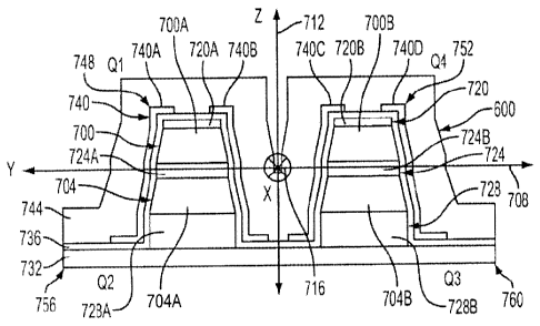
[0030] FIGS. 6 and 7 illustrate a bimorph PME PVEH beam 600 that can be used
for each
of beams 204A-F of PVEH module 104C of FIG. 2. As readily seen in FIG. 6,
bimorph beam
600 is a cantilever beam fixed at one end and free at the other. In this
example, bimorph
beam 600 is a microscale structure formed on a silicon wafer 604 using
fabrication steps
similar to the steps illustrated below in connection with FIGS. 9A-P and 10A-
B. While the
explanation of bimorph beam 600 is to be understood in this context, those
skilled in the art
will readily understand that the basic structure of this bimorph beam could
alternatively be
executed in another size regime, such as a mesoscale regime, by changing the
fabrication
techniques accordingly. Since those skilled in the art will understand the
alternative
fabrication techniques necessary to execute the structure of bimorph beam 600
at another
scale, those alternative techniques do not need to be described herein for
those skilled in the
art to appreciate the broad scope of the present disclosure. The reader is
referred to FIGS.
9A-P and 10A-13 and accompanying text for an explanation of fabrication
techniques suitable
14
4182119 v2
CA 02681173 2013-01-30
for forming microscale bimorph beam 600.
[0031] As best seen in FIG. 7, beam 600 is considered to be "bimorph" because
it has two
distinct and separate piezoelectric layers 700, 704, which are located on
opposite sides of the
neutral axis for bending in the ZX-plane (here set to coincide with the Y-axis
708 of the
global coordinate system). As those skilled in the art will appreciate,
piezoelectric layers 700,
704 are located on opposite sides of neutral axis 708 so that during bending
in the ZX-plane
the entirety of each layer is either positively or negatively strained so as
to avoid internal
electrical charge cancellation in the piezoelectric material that would occur
if a single layer
straddled the neutral axis. If either of piezoelectric layers 700, 704
straddled neutral axis 708
during ZX-plane bending, a portion of that layer would have a positive strain
and another
portion would have a negative strain, with the resultant electrical charges
canceling one
another.
[0032] In this example, each of these layers is split into two portions
700A-B, 704A-B,
with portions 700A, 704A falling on one side of the neutral axis of YX-plane
bending (here,
for convenience set to coincide with the Z-axis 712) and portions 700B, 704B
falling on the
other side of neutral axis 712. The reason for splitting piezoelectric layers
700, 704 in this
manner is to prevent the charge cancellation in parametric mode bending that
would occur if
these layers were continuous across neutral axis 712. As is readily seen in
FIG. 7,
piezoelectric portions 700A, 704A, 704B, 700B can be considered to fall,
respectively, in
quadrants Q1 through Q4 defined by neutral axes 708, 712. In this connection,
it is noted that
while the parametric mode bending occurs in the YZ-plane perpendicular to the
fundamental
mode bending plane (ZX-plane), the actual motion of the free end of bimorph
beam 600
under the influence of a sufficient driving vibration is circular in nature.
Consequently, the
quadrantization of piezoelectric portions 700A-B, 704A-B provides an effective
way to
harvest the charges from these portions quadrant by quadrant. For example,
when the
bending of bimorph beam 600 is purely in the ZX-plane (i.e., about Y-axis
708),
piezoelectric portions 700A-B will be equally strained with one another at one
polarity and
piezoelectric portions 704A-B will be equally strained with one another at the
opposite
polarity. When the bending of bimorph beam 600 is purely in the YX-plane
(i.e., about Z-
axis 712), piezoelectric portions 700A, 704A will be equally strained with one
another at one
4182119 v2
CA 02681173 2013-01-30
polarity and piezoelectric portions 700B, 704B will be equally strained with
one another at
the opposite polarity. When the bending of bimorph beam 600 is in a plane
rotated about the
X-axis 716 to an angle between the YX- and ZX planes, either piezoelectric
portions 700A,
704B or piezoelectric portions 700B, 704A will have the maximum and minimum
opposite
polarity strains, depending on the location of that plane.
100331 Still
referring to FIG. 7, bimorph beam 600 includes three electrode layers 720,
724, 728 split into individual electrodes 720A-B, 724A-B, 728A-B to facilitate
the quadrant-
by-quadrant harvesting of electrical charge from corresponding respective ones
of
piezoelectric portions 700A-B, 704A-13. The fact that electrode layers 720,
724, 728 are split
into individual electrodes 720A-B, 724A-B, 728A-B gives rise to the term
"split-electrode"
used to describe the PME PVEH beams of the present disclosure having this type
of
structure. It is noted that the term "split-electrode" is not, however,
limited to a situation
wherein a single layer or large electrode is split during subsequent
fabrication steps. Rather,
the term "split-electrode" also applies to situations in which separately
formed electrodes are
provided on opposite sides of neutral axis 712. In other words, the "split
electrode" concept
applies to the fact that parametric mode charge harvesting electrodes are
spaced from one
another, rather than to how they are formed.
[0034] More
particularly relative to the functioning of electrodes 720A-B, 724A-B,
728A-B, electrodes 720A, 724A are active in harvesting charge from
piezoelectric portion
700A in quadrant Q1, electrodes 724A, 728A are active in harvesting charge
from
piezoelectric portion 704A in quadrant Q2, electrodes 724B, 728B are active in
harvesting
charge from piezoelectric portion 704B in quadrant Q3 and electrodes 720B,
724B are active
in harvesting charge from piezoelectric portion 700B in quadrant Q4. As is
readily seen,
electrodes 724A-B each straddle neutral axis 712, thereby providing the
separation of
corresponding respective piezoelectric portions 700A-B, 704A-B from neutral
axis 712 that
results in the avoidance of charge cancellation as described above. Referring
to FIG. 6,
bimorph beam 600 may be provided with contacts 608, 612, 616 corresponding
respectively
to electrode layers 720, 724, 728 for communicating the charges collected from
piezoelectric
portions 700A-B, 704A-B (FIG. 7) to appropriate charge collection circuitry
(not shown).
16
4182119 v2
CA 02681173 2013-01-30
[0035] Still referring to FIG. 6, in this embodiment, bimorph beam 600 has a
proof mass
620 located adjacent the free end of the beam. Proof mass 620 is provided to
lower the tuning
of bimorph beam 600 and also to increase the power output of the beam. In
other
embodiments, a proof mass need not be provided at all, while in yet other
embodiments,
more than one proof mass may be provided, for example, at differing locations
along the
bimorph beam. As those skilled in the art will readily appreciate, bimorph
beam 600 can be
tuned by varying any one or more of a number of parameters, such as the cross-
sectional
shape of the beam, cross-sectional dimensions of the beam, the length of the
beam
(exemplary thicknesses), the mass of the proof mass(es), if any, the
location(s) of the proof
mass(es) on the beam, and the materials used to make the beam.
100361 As mentioned above, bimorph beam 600 is made using silicon wafer 604 as
a
substrate. During the fabrication of bimorph beam 600 various layers, such as
electrode
layers 720, 724, 728 and piezoelectric layers 700, 704 are deposited and
etched according to
known techniques. To create free-ended cantilevered bimorph beam 600, one of
the
fabrication steps involves etching away a portion of silicon wafer 604 to
create a cavity 624
beneath the beam and to create the separation between any adjacent bimorph
beam(s) or
other laterally adjacent portion of the wafer. Again, examples of fabrication
steps that can be
used to make bimorph beam 600 are described below in connection with FIGS. 9A-
P and
10A-B.
[0037] Referring to FIG. 7, and also to FIG. 6, other layers included in
bimorph beam 600
of this example include a base layer 732, an optional first insulating layer
736, an optional
side-electrode layer 740 and a second insulating layer 744. Base layer 732 is
provided for use
in forming cavity 634 and is an artifact of that process. First insulating
layer 736 is provided
if optional side-electrode layer 740 is provided. Side-electrode layer 740, if
provided, is
patterned and etched to provide optional side electrodes 740A-D that may be
used in
parametric mode charge harvesting. If provided, each side electrode 740A-D
acts like a
charge plate of a capacitor, wherein first insulating layer 736 acts as the
dielectric of the
capacitor and ones of piezoelectric portions 700A-B, 704A-B act as the other
charge plate.
Optional side electrodes 740A-D may be made of any suitable conductive
material, such as
any one of the materials mentioned above relative to electrode layers 720,
724, 728. Second
17
4182119 v2
CA 02681173 2013-01-30
insulating layer 744 is provided as a protective layer and as a stress
compensation layer to
compensate for stresses induces in bimorph beam 600 by other layers during
fabrication.
[00381 In a specific illustrative, but by no means limiting, example, the
various layers of
bimorph beam 600 are made of the following materials and have the following
thicknesses:
base layer 732 is a thermal oxide of the silicon wafer 604 having a thickness
of 0.5 pm;
electrode layer 728 is a molybdenum (Mo) layer having a thickness of 1.0 pm;
piezoelectric
layer 704 is an aluminum nitride (A IN) layer having a thickness of 1.0 pm;
electrode layer
724 is an Mo layer having a thickness of 0.5 pm; piezoelectric layer 700 is an
MN layer
having a thickness of 1.0 m; electrode layer 720 is an Mo layer having a
thickness of 0.2
1.1,1ri; first insulating layer 736 is a PECVD oxide layer having a thickness
of 0.1 1.1.M to 0.2
m; side-electrode layer 740 is an Mo layer having a thickness of 0.2 ilm; and
second
insulating layer 744 is a PECVD oxide layer having a thickness of 1.8 p.m. Of
course, in
other embodiments, the dimension may vary. In this connection, it is noted
that all thickness
and dimension used herein are illustrative and can be increased or decreased.
For example,
increasing the volume of a PVEH unit of the present disclosure, such as PVEH
unit 100 of
FIG. 1, will increase the output power and voltage (although voltage depends
only on
thickness and length of the piezoelectric layer(s)), yet if done correctly the
resonance
frequency could remain unchanged or be altered if desired. A drawback to
increasing the
volume of a PVEH unit is that fewer modules/chips can be fabricated from a
single wafer,
thus increasing the cost per die.
100391 It is
also noted that the location of neutral axis 712 can be adjusted up and down
(relative to FIG. 7) by changing the thicknesses of the various layers. It is
also noted for
clarity that the angled sidewalls of piezoelectric portions 700A-B, 704A-B and
subsequently
deposited layers is merely an artifact of the etching techniques used in
forming the split-
electrode structure. In other embodiments, these angled sidewalls can be
eliminated by
selection of appropriate fabrication techniques, as can the relatively wide
spacing between
the two stacks 748, 752 and the overhangs 756, 760 that are also artifacts of
the particular
fabrication process used.
18
4182119 v2
CA 02681173 2013-01-30
[0040] Whereas FIGS. 6 and 7 illustrate an example of a bimorph split-
electrode PME
PVEH beam 600, FIG. 8 illustrates a monomorph version 800 of such a beam. As
seen in
FIG. 8, when monomorph beam 800 is made to the same microscale and is made
using the
same fabrication processes as bimorph beam 600 of FIGS. 6 and 7, monomorph
beam 800
may be constructed very similarly to bimorph beam 600. However, instead of
having two
piezoelectric layers 700, 704 (FIG. 7) and three electrode layers 720, 724,
728, monomorph
beam 800 of FIG. 8 has only a single piezoelectric layer 804 and a pair of
electrode layers
808, 812 sandwiching the piezoelectric layer therebetween. Each of these
layers 804, 808,
812 is "split" horizontally (relative to FIG. 8) so as to provide two
monomorph charge
generators 816, 820 electrically decoupled from one another for the reasons
discussed above
relating to the harvesting of charge from parametric mode excitation of beam
800. In this
example, fundamental resonance excitation occurs in the ZX-plane, and
parametric mode
excitation occurs in the YZ-plane, as it did in bimorph beam 600 of FIGS. 6
and 7. With the
splitting of layers 804, 808, 812, stack 816 contains piezoelectric portion
804A and
corresponding electrodes 808A, 812A, and stack 820 contains piezoelectric
portion 804B and
corresponding electrodes 808B, 812B.
[0041] To avoid charge cancellation within piezoelectric layer 804 during
bending in the
ZX- plane, the thicknesses of the various layers of monomorph beam 800 are
chosen so that
the entirety of the piezoelectric layer lies on one side or the other of the
neutral bending axis,
here to which the global Y-axis 824 is set for convenience. In this manner,
during ZX-plane
bending, the entirety of piezoelectric layer 804 is strained either positively
or negatively.
Similar to bimorph beam 600 of FIGS. 6 and 7, charge cancellation within
piezoelectric layer
804 is avoided by splitting layers 804, 808, 812 so that stacks 816, 820 lie
on opposite sides
of the neutral axis, here global Z-axis 826.
[0042] Electrodes 808A-B may be electrically tied to one another beyond the
fixed end of
monomorph beam 800 (see FIG. 6, which can be used to envision a cantilever
configuration
of monomorph beam 800), as may electrodes 812A-B. Then, monomorph beam 800 may
be
provided with electrical contacts (not shown) in a manner similar to
electrical contacts 608,
612, 616 (FIG. 6) of bimorph beam 600.
19
4182119 v2
CA 02681173 2013-01-30
[0043] As with bimorph beam 600, monomorph beam 800 may have various layers in
addition to piezoelectric and electrode layers 804, 808, 812. In this example,
such additional
layers include a base layer 828, an optional first insulating layer 832, an
optional side-
electrode layer 836 and a second insulating layer 840. Base layer 828 is an
artifact of the
process used to form monomorph beam 800 and provides a unitary base for stacks
816, 820.
First insulating layer 832 is provided if optional side-electrode layer 836 is
provided. Side-
electrode layer 836, if provided, is patterned and etched to provide optional
side electrodes
836A-D that may be used in parametric mode charge harvesting. If provided,
each side
electrode 836A-D acts like a charge plate of a capacitor, wherein first
insulating layer 832
acts as the dielectric of the capacitor and ones of piezoelectric portions
804A-B act as the
other charge plate. Optional side electrodes 836A-D may be made of any
suitable conductive
material, such as any one of the materials mentioned above relative to
electrode layers 720,
724, 728 of bimorph beam 600 of FIGS. 6 and 7. Second insulating layer 840 is
provided as a
protective layer and as a stress compensation layer to compensate for stresses
induced in
bimorph beam 600 by other layers during fabrication. In this example, first
and second
insulating layers 832, 840 are oxides formed by plasma-enhanced chemical vapor
deposition
(PECVD).
[0044] In a specific illustrative, but by no means limiting, example, the
various layers of
monomorph beam 800 are made of the following materials and have the following
thicknesses: base layer 828 is a thermal oxide of the original silicon wafer
(see FIGS. 6 and 7
and accompanying text) having a thickness of 2.0 pm; electrode layer 812 is an
Mo layer
having a thickness of 1.0 ilm; piezoelectric layer 804 is an A11\1 layer
having a thickness of
1.0 p.m; electrode layer 808 is an Mo layer having a thickness of 0.2 rim;
first insulating layer
832 is a PECVD oxide layer having a thickness of 0.2 p.m; side-electrode layer
836 is an Mo
layer having a thickness of 0.1 vim; and second insulating layer 840 is a
PECVD oxide layer
having a thickness of 1.3 vin. Of course, in other embodiments, the dimension
may vary. It is
noted for clarity that the angled sidewalls of piezoelectric portions 804A-B
and subsequently
deposited layers is merely an artifact of the etching techniques used in
forming the split-
electrode structure. In other embodiments, these angled sidewalls can be
eliminated by
selection of appropriate fabrication techniques, as can the relatively wide
spacing between
4182119 v2
CA 02681173 2013-01-30
the two stacks 816, 820 and the overhangs 844, 848 that are also artifacts of
the particular
fabrication process used.
[0045] Though not shown, monomorph beam 800 may include one or more proof
masses
in a manner similar to bimorph beam 600 of FIGS. 6 and 7, if desired or
needed. In addition,
monomorph beam 800 may be tuned for fundamental resonance response using any
one or
more of the techniques mentioned above relative to bimorph beam 600. Further,
the
parametric mode response of monomorph beam 800 can be tuned by varying the
ratio of the
width W' of the beam to the thickness T' of the beam (assuming a substantially
rectangular
cross-sectional shape) as described above in connection with FIG. 4. In the
exemplary
microscale construction of monomorph cantilever beam 800 described above,
upward curling
of the beam occurs as a result of strain induced in the upper portion of the
beam by
piezoelectric layer 804. This curling can be controlled to be within tolerable
limits using
appropriate techniques. It is noted that bimorph beam 600 of FIGS. 6 and 7 has
less tendency
to curl due to the presence of piezoelectric layers 700, 704 on opposite sides
of ZX-bending
neutral axis 708.
[0046] FIGS. 9A-P illustrate steps that can be used to fabricate a microscale
cantilever
monomorph PME PVEH beam, such as beam 800 of FIG. 8, and indeed an entire
microscale
PVEH module, such as any one of modules 104A-P of FIGS. 1 and 2. At step 900
(FIG. 9A),
a silicon substrate 902 is provided. Silicon substrate 902 may have any
crystal orientation
and any dopant type and doping concentration. At step 904 (FIG. 9B), a base
layer 906 is
provided to substrate 902. Base layer 906 corresponds to base layers 828 of
FIG. 8,
respectively, and, as mentioned above, are used as etch stops for creating the
cantilever of
beam 800 (FIG. 8). Base layer 906 can be, for example: 1) a grown thermal
silicon dioxide
(Si02); 2) a low-pressure chemical vapor deposition (LPCVD) or plasma-enhanced
CVD
(PECVD) silicon oxide (SiOx, X <1= 2); or a low-stress silicon-rich nitride
(SixNy, X < 3, Y
<4). Base layer 906 can be provided to both sides of silicon substrate 902 to
balance thin-
film stress.
[0047] At
step 908 (FIG. 9C), a metal layer 910 is deposited via sputtering or
evaporation
on one side of substrate 902. Metal layer 910 corresponds to electrode layer
812 of
21
4182119 v2
CA 02681173 2013-01-30
monomorph beam 800 of FIG. 8. At step 912, a piezoelectric layer 914 is
deposited on one
side of substrate 902. The piezoelectric material used for this layer 914 may
be, for example,
any of AIN (deposited by sputtering), lead zirconate titanate (PZT) (deposited
via a Sol gel
process or sputtering), polyvinylidene fluoride (PVDF) (deposited via a Sol
gel process) and
zinc oxide (ZnO) (deposited via sputtering). At step 916 (FIG 9E), a second
metal layer 918,
corresponding to electrode layer 808 of monomorph beam 800 of FIG. 8, is
deposited via
sputtering or evaporation.
[0048] At step 920 (FIG. 9F), second metal layer 918 is patterned, for
example, using
photolithographic patterning techniques, and then etched using a wet etch or
dry reactive ion
etch (RIE). At step 922 (FIG. 9G), piezoelectric layer 914 is etched using a
wet etch or dry
RIE. If A 1I\1 is used for piezoelectric layer 914 and Mo is used for metal
layers 910, 918, a
wet potassium hydroxide (KOH) process can be used. In this case, the
photoresist (not
shown) from the patterning of step 920 is stripped prior to the KOH etch and
the Mo of metal
layers 910, 918 is used as a hard mask. AIN etches anisotropically in KOH and
forms the
angled walls highlighted relative to each of FIGS. 7 and 8, above. At step 924
(FIG. 911),
metal layer 910 is etched using a wet etch or dry RIE. In the Mo example just
noted, Mo uses
RIE.
[0049] At step 926 (FIG. 91), a first upper dielectric 928, which corresponds
to first
insulating layer 836 of monomorph beam 800 of FIG. 8, is deposited. Dielectric
928 can be,
for example, a deposited LPCVD or PECVD silicon oxide (Si0,) or silicon
nitride (SiõNy).
Typically, metals are not put into an LPCVD furnace due to metal cross-
contamination with
other products' films. However, it can be done if a dedicated LPCVD system is
used and the
metal melting point is high (the melting point of tungsten and Mo are high and
the melting
point of gold is low). In this example, first upper dielectric 928 is
deposited on both sides of
substrate 902 to balance thin-film stress. At step 930 (FIG. 9J), first upper
dielectric 928 is
etched using a wet etch or RIE.
[0050] If side electrodes, corresponding to side electrodes 840A-D of
monomorph beam
800 of FIG. 8 are being provided, optional step 932 (FIG. 9K) can be
performed. In step 932,
a metal layer 934 is deposited, for example, via sputtering or evaporation,
and then patterned
22
4182119 v2
CA 02681173 2013-01-30
and etched to form side electrodes 938. If side electrodes 938 are not
provided, step 932 and
either steps 926, 930 of FIGS. 9I-J, respectively, or steps 940, 942 of FIGS.
9L-M,
respectively, are eliminated. Following the formation of side electrodes 938,
if any, steps 940
(FIG. 9L), 942 (FIG. 9M) are performed. At step 940, a second upper dielectric
944, which
corresponds to second insulating layer 840 of monomorph beam 800 of FIG. 8, is
deposited.
Dielectric 944 can be, for example, any one of the materials mentioned above
relative to first
upper dielectric 928. In this example, second upper dielectric 944 is
deposited on both sides
of substrate 902 to balance thin-film stress. At step 942 (FIG. 9M), second
upper dielectric
944 is etched using a wet etch or RIE.
[0051] At step 946 (FIG. 9N), electrical contacts 948, 950 and interconnecting
wiring (not
shown) are provided. Typically, though not necessarily, electrical contacts
948, 950 will be
aluminum with about 2% silicon to inhibit electro-migration due to electrical
current flow.
Contacts 948, 950 and wiring may be provided, for example, by either a photo
metal
deposition (evaporation) lift-off process or by deposition (evaporation and
sputtering) and
wet etch or RIE. At step 952 (FIG. 90), a proof mass 954 is formed using a
suitable method.
Generally, electroplating is the best method for achieving thick metal
depositions in the
range of about 10 p.m to about 100 p.m. Evaporation is limited to thicknesses
less than about
3 p.m.
[0052] At step 956 (FIG. 9P), the precursor to cantilever beam 958 is released
from
substrate 902 to form the cantilever. In this example, cantilever beam 958 is
formed using a
backside release method that involves patterning and etching through second
and first
dielectrics 944, 928 and backside base layer 906 and then performing a deep
RIE (DRIE)
through substrate 902 to the underside of the frontside base layer.
[0053] FIGS. 10A-B illustrate two alternative methods of releasing the
precursor structure
to the cantilever beam, both involving etching from the front side of the
assembly, rather than
from the backside as just described relative to FIG. 9P. In FIG. 10A, a
silicon isotropic etch
is performed from the front side of the assembly 1000 to form a cavity 1004
beneath
cantilever beam 1008. For example, a fluorine-based etchant, such as gaseous
xenon fluoride
(XeF2) or sulfur Hexafluoride (SF6), that etches silicon isotropically but
does not attack other
23
4182119 v2
CA 02681173 2013-01-30
material may be used. In this type of method, cavity 1004 may limit up-and-
down movement
of the free end of cantilever beam 1008, but the cavity provides isolation for
wafer-scale
packaging and a bottom stop that can be useful in preventing over-flexing
(over-straining) of
the beam. In this case, some upward curl due to asymmetric may be desirable
for "tuning" the
range of motion of the free end of cantilever beam 1008.
[0054] FIG.
10B illustrates another frontside method of releasing the precursor to the
cantilever beam 1012. In this method, instead of substrate 902 (FIG. 9A) being
a
conventional non-silicon-on-insulator (non-SOI) substrate, an SOI substrate
1016 having a
buried oxide (BOX) layer 1020 can be used. In this method, BOX layer 1020 acts
as an etch
stop to precisely control the depth of the cavity 1024 formed during isotropic
etching from
the front side of SOI substrate 1016. As with the method of FIG. 10A, a
fluorine-based
etchant, such as gaseous XeF2 or SF6, that etches silicon isotropically but
does not attack
other material may be used. Here, too, some upward curl due to asymmetric may
be desirable
for "tuning" the range of motion of the free end of cantilever beam 1012.
[0055] While the fabrication techniques of FIGS. 9A-P and 10A-B are directed
to making
monomorph beams 958, 1008, 1012, these techniques can be readily extended for
producing
bimorph beams similar to bimorph beam 600 of FIGS. 6 and 7. For example,
rather than
patterning and etching second metal layer 918, first piezoelectric layer 914
and first metal
layer 910 at steps 920, 922, 924 of FIGS. 9F-H, just after the deposition of
the second metal
layer at step 916 (FIG. 9E), instead a second piezoelectric layer (not shown,
but
corresponding to piezoelectric layer 700 of FIG. 7) and a third metal layer
(also not shown,
but corresponding to electrode layer 712 of FIG. 7) can be deposited on the
second metal
layer before continuing with the deposition of first upper dielectric 928, as
in step 926 of
FIG. 91. Then, the etching starts with the third metal layer and proceeds down
to, and
includes, first metal layer 910. During this process, it may be desirable to
alter the
thicknesses of upper dielectrics 944, 928 and base layer 906 to balance
stresses and control
curling as desired or necessary.
[0056] As
mentioned above, a PVEH unit made in accordance with concepts disclosed
above may be used in any of a variety of applications, including wireless
sensor applications.
24
4182119 v2
CA 02681173 2013-01-30
FIG. 11 illustrates an exemplary wireless sensor 1100 that comprises a
standalone power
supply 1104 that includes a PVEH unit 1108 that is generally of similar
construction to
PVEH unit 100 of FIG. 1. That is, PVEH unit 1108 includes a plurality of
groups (not
shown) of PME beams (not shown). Although not shown, the groups may, but need
not
necessarily be laid out similar to groups 200A-E of FIG. 2A and each of the
PME beams may
be, for example, similar to bimorph beam 600 shown in FIGS. 6 and 7 or
monomorph beam
800 shown in FIG. 8. In this example, PVEH unit 1108 has PME beams having
three
differing tunings tuned in the manner described above relative to FIGS. 4 and
5 so as to
broaden the effective bandwidth of the PVEH unit around a target frequency. In
FIG. 11, the
like-tuned beams are identified as a first set 1112, a second set 1116 and a
third set 1120, and
the sets have corresponding respective differing fundamental resonance
frequencies Viii,
VB2, VB2 and corresponding respective differing parametric mode frequencies
Vpi, VP2, VP2.
[0057] To optimize the performance of power supply 1104, sets 1112, 1116, 1120
of like-
tuned beams are electrically isolated from one another using suitable
isolation circuitry, such
as, for example, corresponding respective full-bridge rectifiers 1124, 1128,
1132 (here, diode
rectifiers as an example) that inhibit any inactive set(s) (e.g., because they
are not sufficiently
excited by the ambient driving vibration) from draining electrical power from
the active
set(s). In this manner, the maximum amount of power is output from PVEH unit
1108. Those
skilled in the art will understand that other isolation circuitry may be used.
Power supply
1104 also includes one or more electrical storage devices 1136 that store
electrical energy
scavenged by PVEH unit 1108 for use by other electronics aboard wireless
sensor. Each
electrical storage device 1136 may be any suitable rechargeable device, such
as a super-
capacitor (also "ultra-capacitor") or a rechargeable battery, for example, and
lithium-ion
battery, among others. In this example, power supply 1104 has only a single
PVEH unit 1108
for scavenging vibration from a driving ambient vibration in one direction. It
is noted that
one or more additional, like PVEH units (not shown) could be provided in one
or more
differing orientations for scavenging vibrations in another direction.
100581 In
this example, wireless sensor 1100 includes one or more transducers 1140, such
as a pressure transducer, accelerometer, temperature probe, etc., as the
application for the
wireless sensor requires. Wireless sensor 1100 further includes a
microcontroller 1144 for
4182119 v2
CA 02681173 2013-01-30
controlling the operation of the wireless sensor and a radio transmitter or
transceiver 1148 for
allowing the wireless sensor to communicate with one or more other devices,
such as another
like wireless sensor, a repeater, an information collection node device or a
base-station
device, among others. In addition to or in place of microcontroller 1144,
wireless sensor
1100 may include one or more microprocessors that provide the wireless sensor
with higher
level data processing functionality, if desired. In this embodiment, power
supply 1104
provides electrical power to each transducer 1140, microcontroller 1144 (or
microprocessor)
and transceiver 1148. Those skilled in the art will understand that each
transducer 1140,
microcontroller 1144 (or microprocessor) and transceiver 1148 can be of a
conventional
design and, therefore, need not be described in detail herein.
[0059] FIG. 12 illustrates a wireless sensor network 1200 that includes a
plurality of
sensor nodes 1204A-G and a central station 1208. Each of sensor nodes 1204A-G
in this
example includes a standalone PME PVEH power supply (not shown) and is similar
to
wireless sensor 1100 of FIG. 11. In this example, sensor nodes 1204A-F may be
considered
terminal nodes, whereas sensor node 12040 may be considered an intermediate
node. In this
context, a terminal node generally only collects its own sensed data and
transmits it to either
another node (such as intermediate sensor 1204G) or central station 1208.
Depending on
whether the network is of a push type or a pull type (and/or for other
reasons) a terminal
node may also receive information, such as a pull request, from central
station 1208 or
another node, such as intermediate sensor 1204G. Intermediate sensor 1204G, on
the other
hand is continually both receiving data, here from sensor nodes 1204D-F, and
sending data to
central station 1208. Those skilled in the art will readily understand how to
configure sensor
nodes 1204A-G and central station 1208 for proper operation in the context of
the sensors
nodes having PME PVEH units of the present disclosure.
[0060] Exemplary embodiments have been disclosed above and illustrated in the
accompanying drawings. The scope of the claims should not be limited by the
preferred
embodiments set forth above, but should be given the broadest interpretation
consistent with
the description as a whole.
26
4182119 v2