Note: Descriptions are shown in the official language in which they were submitted.
CA 02681353 2009-09-18
METHOD AND APPARATUS FOR MANUFACTURING SILICON INGOT
BACKGROUND OF THE INVENTION
Field of the Invention
[0001]
This invention relates to a method and apparatus for manufacturing a silicon
ingot suitable for the production of solar cells.
Description of the Related Art
[0002]
Nowadays, demand for high-purity silicon has been increasing with a
remarkable increase in the production quantity of solar cells. In the
production of solar
cells, off-specification products of semiconductor silicon, scraps thereof,
and others are
usually used as raw material. However, in order to cope with an expectable
increase in
the production quantity of solar cells in the future, required are a
manufacturing method
and a manufacturing apparatus making it possible to attain mass production of
inexpensive silicon for solar cells, which aims for stable supply. Hitherto,
in this
technical field, methods have been developed for refining inexpensive metallic
silicon
metallurgically at high temperature in a long time; however, costs therefor
have been
desired to be made lower.
[0003]
A method that is one of the metallurgically refming methods and that is for
refining silicon for a solar cell (SOG) effectively is suggested in, for
example, Japanese
Patent No. 3325900.
[0004]
JP-A No. 2003-286024 suggests a method of putting only a silicon having a
higher purity than metallic silicon, as a material, into a crucible, melting
this material,
1
CA 02681353 2009-09-18
and then producing a silicon ingot therefrom by a pulling method.
[0005]
JP-A No. 2003-277040 suggests a method of raising the purity of a metallic
silicon although the document does not refer to any method for producing an
ingot.
[0006]
JP-A No. 2002-047095 suggests a method of doping silicon with aluminum,
and then producing a silicon ingot therefrom by a pulling method. In this
technique, a
eutectic phenomenon is not used.
[0007]
JP-A No. 10-273313 suggests, as an inexpensive manufacturing method which
targets silicon for a solar cell (SOG), a method of solidifying a molten metal
in a mold
along one direction from the lower region of the metal to the upper region
thereof while
scanning an electron beam onto the surface of the metal to heat the surface.
SUMMARY OF THE INVENTION
[0008]
An object of the present invention is to provide a silicon ingot manufacturing
method at low costs that is suitable for the production of a silicon ingot for
solar cells,
and a manufacturing apparatus used in this method.
[0009]
According to this invention, a success has been achieved in the production of
a
silicon polycrystal or silicon monocrystal for solar cells directly from a
metallic silicon
by a pulling method. The metallic silicon has a purity of about 98% to 99%, so
as to
have an impurity element. In the invention, a solvent metal which can undergo
alloy
reaction with silicon is selected, thereby making it possible to attain a
crystal-pulling
process in a silicon melting temperature set into a remarkably lower
temperature range
than an ordinary silicon melting temperature, which is 1412 C. Furkhermore,
the
2
CA 02681353 2009-09-18
above-mentioned problems have been solved by adding a new function to a CZ
type
crystal-pulling apparatus for taking out a middle-purity silicon crystal from
a molten
silicon alloy.
[0010]
In order to attain the object, the method suggested by this invention, for
manufacturing a silicon ingot, is a method including the step of heating and
melting, in
a crucible, an element which can undergo eutectic reaction with silicon and
has a lower
eutectic point than the melting point of silicon when made into silicon alloy,
and a
metallic silicon, thereby generating an alloy melt, and the step of using the
eutectic
reaction for the alloy melt to subject the silicon to low-temperature
solidification
refinement, and further producing the silicon ingot from the alloy melt by a
pulling
method.
[0011]
It is desired in the method that the liquid temperature of portions of the
alloy
melt other than the liquid surface thereof is kept into temperatures at which
the alloy
melt is not solidified, and the liquid surface temperature of the alloy melt
is kept into
temperatures close to a primary crystallization temperature of the alloy melt
which
corresponds to the concentration of the silicon in the alloy melt.
[0012]
It is also desired in the method that the liquid surface temperature of the
alloy
melt is kept at a temperature that is between the eutectic point and a
temperature close
to 1273 K and is close to the primary crystallization temperature of the alloy
melt which
corresponds to the concentration of the silicon in the alloy melt.
[0013]
As described above, the invention makes it possible to manufacture a silicon
ingot directly from a metallic silicon as a raw material. In this way, the
manufacturing
process can be made simple, and costs therefor can be made low.
3
CA 02681353 2009-09-18
[0014]
The metallic silicon may be a silicon having a purity of 98% or more, which
has been hitherto used to manufacture a silicon ingot for solar cells.
[0015]
In the invention, an element which can undergo eutectic reaction with silicon
and has a lower eutectic point than the melting point of silicon when made
into silicon
alloy, and a metallic silicon are heated and melted in a crucible to generate
an alloy melt.
This makes it possible to solidify the melt at a temperature lower than the
melting point
of silicon (1414 C=1687 K), and decrease the power consumption required for
the
manufacture of silicon ingots. In short, the solidification temperature is
changed by
the eutectic reaction, thereby lowering the solidification temperature, so
that the power
consumption can be restrained.
[0016]
As shown in FIG. 4 (source: F. A. Trumbore, Bell System Technical Journal, 39
(1960), 67.), the solid solubility of an impurity element in silicon exhibits
the following
unique behavior: the solid solubility increases as the temperature is lowered
from the
melting point, 1687 K(1414 C), of silicon; and the solid solubility decreases
from
temperatures in the range of 1473 K(1200 C) to 1273 K(1000 C).
[0017]
Table 1, which will be described later, shows results of the segregation
coefficient of each impurity element in Si-Al melt and solid silicon, the
results being
obtained from an experiment wherein aluminum is used as an element which can
undergo eutectic reaction with silicon and has a lower eutectic point than the
melting
point of silicon when made into silicon alloy. The segregation coefficient
denotes "the
ratio of the impurity concentration in the liquid phase to that in the solid
phase". The
source thereof is as follows: ISIJ International, Vol. 45 (2005), No. 7, pp.
967-971
Refining of Si by the Solidification of Si-Al Melt with Electromagnetic Force.
As the
4
CA 02681353 2009-09-18
segregation coefficient is smaller, the impurity in the solidified silicon is
discharged into
the side of the liquid phase, which is a solvent, so that a solid silicon
having a higher
purity can be obtained.
[0018]
As shown in Table 1, the segregation coefficient is varied in accordance with
the primary crystallization temperature of silicon. Therefore, when the melt
is
solidified in an environment giving an optimal primary crystallization
temperature, a
high-purity solid silicon can be produced through refinement.
[0019]
As will be described later, the primary crystallization temperature of the
melt
and the silicon concentration in the melt have a corresponding relationship.
Thus,
when the silicon concentration is adjusted, a high-purity solid silicon can be
produced
through refinement.
[0020]
When, for example, aluminum is used as an element which can undergo
eutectic reaction with silicon and has a lower eutectic point than the melting
point of
silicon when made into silicon alloy, the phase diagram of Si-Al eutectic
alloy is shown
in FIG 2. In FIG 2, L represents the liquid phase; (3, the solid phase of
silicon; a, the
solid phase of aluminum; and A, the eutectic point (850 K=577 C). Reference
number
1 represents the primary crystallization curve. The primary crystallization
curve 1,
which represents the primary crystallization temperature of the melt, and the
silicon
concentration in the melt have a corresponding relationship.
[0021]
When Si is solidified from a Si-Al alloy melt to the crystal side along the (3
phase (Al is solid-dissolved in Si) liquidus line, it is necessary to make the
concentration in the Si-Al alloy constant. By controlling the Si concentration
and the
Al concentration in the Si-Al alloy melt, the precipitation temperature of Si
is decided.
CA 02681353 2009-09-18
[0022]
Thus, about the alloy used in the invention, which is composed of an element
which can undergo eutectic reaction with silicon and has a lower eutectic
point than the
melting point of silicon when made into silicon alloy, and a metallic silicon,
a phase
diagram as shown in FIG 2 is prepared beforehand.
[0023]
In the process for carrying out the manufacturing method of the invention, the
silicon concentration in the melt is measured while the surface of the melt is
kept in a
supercooled liquid state. In other words, the liquid surface temperature of
the melt is
kept into temperatures close to a primary crystallization temperature of the
melt (for
example, the primary crystallization curve temperature represented by
reference number
1 in FIG. 2) which corresponds to the measured silicon concentration in the
melt, for
example, at a temperature close to and below the line. Naturally, it is
necessary to
keep the liquid temperature of the melt portion other than the surface of the
melt into
temperatures at which the melt is not solidified.
[0024]
As described above, in the method of the invention, by a pulling method, a
seed crystal immersed beforehand into the liquid surface is pulled up from the
melt
surface that is in the middle of a transition from the supercooled liquid
phase to solid
phase. In this way, the silicon crystal is grown. At this time, by the
property that the
segregation coefficient of silicon is small, the impurities are discharged
into the solvent
liquid phase so that a high-purity silicon crystal grows around the seed
crystal. Thus, a
silicon ingot can be obtained.
[0025]
When an attempt is made for crystallizing a melt in a crucible without pulling
up any crystal in the prior art, the melt is not turned into an ingot state,
thereby causing
a problem that a needle crystal is generated so as to be scattered (with
reference to "ISIJ
6
CA 02681353 2009-09-18
International, Vol. 45 (2005), No. 7, pp. 967-971 Refining of Si by the
Solidification of
Si-Al Melt with Electromagnetic Force"). The invention has solved this problem
by a
pulling method, and succeeded in making a melt into an ingot.
[0026]
For the method for manufacturing a silicon ingot according to the invention,
it
is important what (value) is the silicon concentration in the alloy melt, that
is, the ratio
of an element which can undergo eutectic reaction with silicon and has a lower
eutectic
point than the melting point of silicon when made into silicon alloy, and a
metallic
silicon, both of which are to be put into a crucible.
[0027]
Firstly, it is more preferred from the viewpoint of electric power saving that
the
silicon concentration is lower since the melting point of silicon becomes
lower with a
decrease in the concentration thereof.
[0028]
Secondly, in connection with an increase in the purity, there is a unique
behavior that as the temperature is lowered than temperatures close to 1273
K(1000 C),
the solid solubility of the impurity elements is decreased. When the alloy
melt is
solidified, a larger amount of the impurities is discharged into the solvent
liquid phase.
[0029]
Thirdly, when the solidification of the silicon is advanced by the pulling
method, the silicon concentration in the alloy melt is naturally lowered, so
that the
concentration falls below a silicon concentration corresponding to the
eutectic point.
In this case, no silicon crystal can be taken out.
[0030]
In light of the first and second points, it is desired to charge, into a
crucible, an
element which can undergo eutectic reaction with silicon and have a lower
eutectic
point than the melting point of silicon when made into silicon alloy, and a
metallic
7
CA 02681353 2009-09-18
silicon at such a ratio that the silicon concentration is made as low as
possible.
However, according to the third point, the amount of the crystal that can be
taken out
becomes small when the silicon concentration is originally low.
[0031]
In light of the above-mentioned matters, it is desired to charge, into a
crucible,
an element which can undergo eutectic reaction with silicon and has a lower
eutectic
point than the melting point of silicon when made into silicon alloy, and a
metallic
silicon at such a ratio that the silicon concentration gives a melting point
at a
temperature close to 1273 K(1000 C).
[0032]
In the silicon ingot manufacturing method of the invention, for example,
aluminum or copper may be used as the element, which can undergo eutectic
reaction
with silicon and has a lower eutectic point than the melting point of silicon
when made
into silicon alloy.
[0033]
In the silicon ingot manufacturing method of the invention, the step of
generating the alloy melt and the step of producing the silicon ingot are
performed in
the atmosphere of an inert gas, for example, the atmosphere of argon gas.
[0034]
This manner makes it possible to prevent the oxidation of the silicon and
further prevent the oxidation of the element, which can undergo eutectic
reaction with
silicon and has a lower eutectic point than the melting point of silicon when
made into
silicon alloy, for example, aluminum, so that a decline in the efficiency of
absorbing the
impurities can be prevented. This makes it possible to manufacture a high-
purity
silicon ingot which has a higher purity and is more suitable for being used
for solar
cells.
[0035]
8
CA 02681353 2009-09-18
For the same reason, the crucible can be a crucible made not of quartz, which
is
ordinarily used, but of silicon nitride.
[0036]
In order to attain the object, the apparatus for manufacturing a silicon ingot
that
is next suggested by this invention is an apparatus used in the method for
manufacturing
the silicon ingot of the invention and provided with a container to which a
vacuum
exhaust system and a gas introducing system are connected, a crucible set in
the
container, a heating means for heating the crucible to generate an alloy melt
in the
crucible, a pulling-up means for making a silicon crystal in an ingot form,
and a liquid
surface temperature measuring means for measuring the liquid surface
temperature of
the alloy melt in the crucible.
[0037]
The heating means has a function of heating the region of the liquid surface
of
the alloy melt generated in the crucible, and other region of the alloy melt
at intensities
independent of each other.
[0038]
The apparatus of the invention for manufacturing a silicon ingot has a
controlling means for grasping the amount of a fall in the concentration of
silicon in the
alloy melt, and further controlling the heating based on the heating means to
keep the
liquid surface temperature of the alloy melt into temperatures close to a
primary
crystallization temperature which corresponds to the grasped silicon
concentration in
the alloy melt.
[0039]
As described above, in the apparatus of the invention for manufacturing a
silicon ingot, the following are connected to a container in which a crucible
is set: a
vacuum exhaust system; and a gas introducing system (a gas introducing system
for
introducing an inert gas, such as argon gas, into the container). This manner
makes it
9
CA 02681353 2009-09-18
possible to prevent the oxidation of silicon, and further prevent the
oxidation of an
element which can undergo eutectic reaction with silicon and has a lower
eutectic point
than the melting point of silicon when made into silicon alloy, for example,
aluminum,
so that a decline in the efficiency of absorbing impurities can be prevented.
[0040]
The heating means is capable of: making a metallic silicon and an element
which can undergo eutectic reaction with silicon and has a lower eutectic
point than the
melting point of silicon when made into silicon alloy, for example, aluminum,
both of
which are charged into the crucible, into an alloy melt; and further
conducting a liquid
temperature control described below. The liquid temperature control is a
function of
heating the two regions, the liquid surface of the alloy melt in the crucible,
and the other
region of the alloy melt at intensities independent of each other. The liquid
temperature control through the heating means is carried out by manual
operation,
and/or automatic operation based on programming.
[0041]
In the controlling means, the function of grasping the amount of a fall in the
silicon concentration in the alloy melt is a function of calculating out the
fall amount of
the silicon concentration in the melt, for example, based on the weight of the
silicon
ingot pulled up by the pulling-up means, which will be described later.
[0042]
The function of controlling the heating based on the heating means in the
controlling means in such a manner that the liquid surface temperature of the
alloy melt
is kept into temperatures close to a primary crystallization temperature which
corresponds to the grasped silicon concentration in the alloy melt is a
function of
outputting a command for heating the crucible with reference to the following:
the
liquid surface temperature of the alloy melt in the crucible, the temperature
being
measured by the liquid surface temperature measuring means; and the fall
amount of the
CA 02681353 2009-09-18
silicon concentration in the alloy melt, which has been grasped as described
above. In
accordance with this output, the heating based on the heating means is
controlled so as
to keep the liquid surface temperature of the alloy melt in the crucible into
temperatures
close to the primary crystallization temperature corresponding to the grasped
silicon
concentration in the alloy melt, that is, so as to keep the liquid surface
into a
supercooled liquid state and further keep the melt portion other than the
liquid surface
in a liquid phase.
[0043]
About the alloy melt that can undergo eutectic reaction, the primary
crystallization temperature thereof is also varied in accordance with a change
in the
concentration of the melt. In the invention, the silicon concentration in the
melt is
decreased by the precipitation of silicon crystal; therefore, it is required
to measure the
silicon concentration in the melt.
[0044]
In the controlling device, a silicon primary crystallization temperature
corresponding to any silicon concentration is stored. When the device receives
information on the present silicon concentration and the present liquid
surface
temperature, the device can output, to the heating means, a heating command
for
keeping the present supercooled liquid state of the melt surface.
[0045]
The pulling-up means in the silicon ingot manufacturing apparatus of the
invention is generally the means adopted when a monocrystal silicon ingot in a
semiconductor grade is manufactured from polycrystal silicon as a raw
material.
[0046]
In the invention, the pulling-up means, which is known in the prior art, is
used
to make silicon crystal into an ingot form. By immersing a seed crystal into
the liquid
surface of the alloy melt, rotating the crystal, and then making a pulling-up
operation
11
CA 02681353 2009-09-18
slowly, a silicon crystal solidified around the seed crystal is grown.
[0047]
In other words, the pulling-up means in the silicon ingot manufacturing
apparatus of the invention is a means which exhibits a function of keeping the
liquid
surface into a supercooled liquid state through the heating means and the
controlling
means, and further making the liquid surface of the alloy melt, the liquid
phase of which
is kept in the melt portion other than the liquid surface, into an ingot form.
Advantageous effects
[0048]
According to this invention, provided can be a method for manufacturing a
silicon ingot at low costs wherein a metallic silicon is used as a raw
material to
manufacture the silicon ingot directly, the method being suitable for
manufacturing a
silicon ingot for solar cells; and a manufacturing apparatus used in this
method.
[0049]
By heating and melting, in a crucible, an element which can undergo eutectic
reaction with silicon and has a lower eutectic point than the melting point of
silicon
when made into silicon alloy, and a metallic silicon, an alloy melt is
generated, thereby
making it possible to solidify the melt at a lower temperature than the
melting point of
silicon (1414 C=1687 K), and decrease power consumption required for
manufacturing
a silicon ingot.
BRIEF DESCRIPTION OF THE DRAWINGS
[0104]
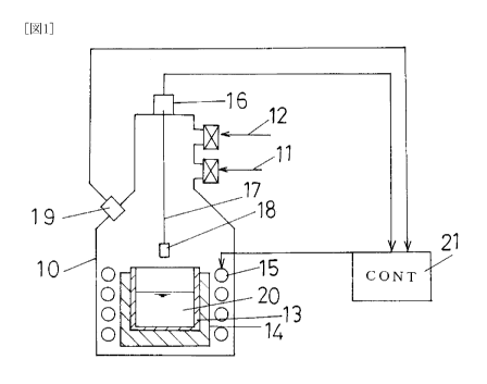
FIG 1 is a view referred to in order to describe a general structure of a
silicon
ingot manufacturing apparatus of this invention;
FIG 2 is a phase diagram of Si-Al eutectic alloy;
FIG 3 is an enlarged view of a portion of the phase diagram of Si-Al eutectic
12
CA 02681353 2009-09-18
alloy;
FIG 4 is a graph showing the solid solubility of each impurity element in
silicon;
FIG 5 is a view illustrating an example of a specific structure of another
silicon
ingot manufacturing apparatus of this invention; and
FIG 6 is a graph showing the state of the concentration of Si and that of Al
that
correspond to a temperature change.
DESCRIPTION OF THE PREFERRED EMBODIMENT
[0050]
With reference to the attached drawings, preferred embodiments of the
invention will be described hereinafter.
Example 1
[0051]
FIG 1 is a view illustrating a general structure of a silicon ingot
manufacturing
apparatus of the invention, wherein a manufacturing method of the invention is
carried
out.
[0052]
A vacuum exhaust system 11 and a gas introducing system 12 are connected to
a container 10.
[0053]
A crucible 13 made of silicon nitride is set at the center on the bottom of
the
container 10 in the state that the crucible 13 is held in a graphite crucible
14. A heater
15 is located on the outside of the graphite crucible 14, so that a material
charged in the
crucible 13 can be heated.
[0054]
A pulling-up mechanism 16 having a weight-measuring function is set on the
13
CA 02681353 2009-09-18
top of the container 10. From this pulling-up mechanism 16 toward the crucible
13, a
freely-rotatable axis 17 is extended.
[0055]
A seed crystal 18 may be fitted to the bottom end of the axis 17.
[0056]
In a side wall of the container 10 a two-wavelength type radiation thermometer
19 is set, so that the surface temperature of a melt 20, which is heated and
melted in the
crucible 13, can be measured.
[0057]
The heater 15 is connected to a controlling device 21 set in the outside of
the
container 10.
[0058]
The controlling device 21 can gain information on the weight of a silicon
ingot
pulled up from the pulling-up mechanism 16, which has a weight-measuring
function,
by an intermediary aid of the seed crystal 18 and information on the surface
temperature
of the melt 20, which is measured by means of the two-wavelength type
radiation
thermometer 19.
[0059]
The heater 15 is formed to make, into an alloy melt, a metallic silicon and an
element which can undergo eutectic reaction with silicon and has a lower
eutectic point
than the melting point of silicon when made into silicon alloy, for example,
aluminum,
the metallic silicon and the element being charged in the crucible 13, and
further formed
to receive a control based on the controlling device 21 to heat the alloy melt
at
intensities independent of each other in two regions that are the liquid
surface of the
alloy melt in the crucible 13 and other melt region.
[0060]
Specifically, the controlling device 21 calculates out the amount of a fall in
the
14
CA 02681353 2009-09-18
silicon concentration in the melt 20 in the crucible 13 from the weight of the
silicon
ingot pulled up by the pulling-up mechanism 16, which has a weight-measuring
function; decides the electric power to be supplied to the heater 15 in such a
manner that
the liquid surface temperature of the melt 20 is kept into temperatures close
to a primary
crystallization temperature corresponding to the calculated silicon
concentration in the
melt 20, preferably at a temperature below and close to the primary
crystallization
temperature, and further the melt portion other than the liquid surface is
kept in the
liquid phase; and controls the heating based on the heater 15.
[0061]
The manufacturing apparatus constructed as described above is used to
manufacture a silicon ingot by the method of the invention, general
information of
which will be described hereinafter.
[0062]
First, a metallic silicon and aluminum are charged into the crucible 13 set in
the container 10.
[0063]
The purity of the metallic silicon is set to 98% or more.
[0064]
With reference to the phase diagram of Si-Al eutectic alloy shown in FIGs. 2
and 3, the ratio by weight between the metallic silicon and aluminum to be
charged are
adjusted to set the silicon concentration to X (in FIG. 3) at a point close to
1273 K
(1000 C).
[0065]
After the metallic silicon and aluminum are charged into the crucible 13, the
gas in the container 10 is discharged through the vacuum exhaust system 11
while a
high-purity inert gas (argon gas) is introduced into the container 10 through
the gas
introducing system 12.
CA 02681353 2009-09-18
[0066]
A purpose thereof is to remove oxygen in the container 10, thereby preventing
the oxidation of the silicon, and further prevent a fall in the impurity-
absorbing
efficiency by the oxidation of aluminum. The vacuum exhaust and the
introduction of
the inert gas are continuously conducted during a crucible-heating and a
silicon-ingot-pulling that will be described below.
[0067]
After oxygen in the container 10 is removed as described above, electric power
is supplied to the heater 15 through the controlling device 21 to heat the
inside of the
crucible 13, thereby melting the charged metallic silicon and aluminum to
generate a
Si-Al eutectic alloy melt.
[0068]
Through the two-wavelength type radiation thermometer 19, the temperature of
the liquid surface of the melt 20 is monitored and the temperature is
controlled, so as to
keep the liquid surface temperature at the primary crystallization temperature
and
continue to control the heating until the metallic silicon and aluminum
charged into the
crucible 13 are completely melted.
[0069]
After the material in the crucible 13 is completely melted, the axis 17
extended
from the pulling-up mechanism 16 is lowered to immerse the seed crystal 18
into the
Si-Al melt and then rotate the seed crystal 18 slowly.
[0070]
Next, the pulling-up mechanism 16 is used to pull up the seed crystal 18
slowly
to grow the silicon crystal by an intermediary aid of the seed crystal 18.
[0071]
By the pulling-up of the silicon ingot, the silicon concentration in the Si-Al
melt 20 falls; however, the controlling device 21 calculates the silicon
concentration and
16
CA 02681353 2009-09-18
further controls the electric power to be supplied to the heater 15, using, as
a target
value at any time, a temperature close to (and slightly below) a primary
crystallization
curve 1 corresponding to the calculated Si concentration in the Si-Al melt 20
in such a
manner that the surface temperature of the Si-Al melt 20 is kept into
temperatures close
to a primary crystallization temperature corresponding to the calculated Si
concentration
in the Si-Al melt 20 so as to keep the surface temperature of the Si-Al melt
20 in a
supercooled liquid state.
[0072]
The segregation coefficient of each of the impurity element in the Si-Al melt
and the solid silicon (silicon crystal) was obtained in an experiment. The
results in
Table 1 were obtained. From the results, it was verified that when silicon was
solidified from the Si-Al melt, the impurities were discharged to the side of
the melt.
[Table 1]
Impurity
Example 2
[0073]
FIG 5 is a view illustrating an example of a specific structure of another
silicon
ingot manufacturing apparatus of the invention, wherein a manufacturing method
of the
invention is carried out.
[0074]
A vacuum exhaust device 31 and an Ar gas introducing device 32 are
connected to a vacuum chamber 30 constituting a crystal growing furnace. As
represented by an arrow 33, a high-purity Ar gas (99.9999%) is supplied to the
Ar gas
introducing device 32. A superhigh-purity Ar gas, the purity of which has been
made
high in the Ar gas introducing device 32, is supplied from above the vacuum
chamber
30 into the vacuum chamber 30, as represented by an arrow 34.
17
CA 02681353 2009-09-18
[0075]
The vacuum exhaust device 31 is composed of, for example, a rotary pump and
a turbo molecular pump.
[0076]
Under a control of a controller 40, high-vacuum exhaust is conducted by the
vacuum exhaust device 31, so that the achieved vacuum in the vacuum chamber 30
will
turn to about 10-3 Pa (at room temperature), for example.
[0077]
An exhaust gas removing device 35 can be connected to the vacuum exhaust
device 31 at the downstream side thereof. When a silicon crystal grows in the
vacuum
chamber 30, silicon oxide, additive oxides, nitrogen monoxide and others are
discharged.
The exhaust gas removing device 35 takes charge of making these gases
nonpoisonous
and then discharging the gases into the atmosphere.
[0078]
An inner crucible 36 made of silicon nitride is set at the center on the
bottom of
the vacuum chamber 30 in the state that the inner crucible 36 is held in an
outer crucible
37 made of graphite. A heater 38 is located on the outside of the outer
crucible 37, so
that a material charged in the inner crucible 36 can be heated. The periphery
of the
heater 38 is covered with a heat shield 39.
[0079]
The heater 38 is composed of an upper heater 3 8a for heating the upper side
of
the outer crucible 37, a middle heater 3 8b for heating the lower side of the
outer
crucible 37, and a lower heater 38c for heating the outer crucible 37 from the
bottom
side thereof.
[0080]
The upper heater 3 8a, the middle heater 3 8b and the lower heater 3 8c are
controlled independently of each other by the controller 40.
18
CA 02681353 2009-09-18
[0081]
This manner is used to make, into an alloy melt, a metallic silicon and an
element which can undergo eutectic reaction with silicon and has a lower
eutectic point
than the melting point of silicon when made into silicon alloy, for example,
aluminum,
the metallic silicon and the element being charged in the inner crucible 36,
and further
to receive a control based on the controller 40 to heat the alloy melt at
intensities
independent of each other in two regions that are the liquid surface of the
alloy melt in
the inner crucible 36 and the other melt region.
[0082]
A pulling-up axis load ce1141 is arranged above the vacuum chamber 30 to
interpose a gate valve 55 therebetween. From the pulling-up axis load ce1141
toward
the inner crucible 36, a freely-rotatable pulling-up shaft 42 is extended. The
pulling-up shaft 42 can be rotated in a direction represented by an arrow 43
and in the
direction reverse thereto, and can further be raised and lowered as
represented by an
arrow 44 under a control of the controller 40.
[0083]
A seed chuck 45, which has a tip (at the bottom end side in FIG 5) to which a
seed crystal is to be fitted, is arranged at the bottom end of the pulling-up
shaft 42.
[0084]
In the state that the seed chuck 45 grasps a seed crystal, the pulling-up
shaft 42
is lowered so that the seed crystal arrives at the melt in the inner crucible
36.
Thereafter, the pulling-up shaft 42 is raised to pull up a silicon crystal. At
this time, an
increase per unit time in the weight of the silicon crystal is detected
through the
pulling-up axis load ce1141. Information on the detected increase per unit
time in the
weight of the silicon crystal is sent to the controller 40, and then used for
a control of
the apparatus by the controller 40.
[0085]
19
CA 02681353 2009-09-18
With reference to, for example, the increase per unit time in the weight of
the
silicon crystal, the increase being detected through the pulling-up axis load
cell 41, the
controller 40 calculates out the amount of a fall in the silicon concentration
in the Si-Al
alloy melt in the inner crucible 36; decides the electric power to be supplied
to the
heater 38 (the upper heater 3 8a, the middle heater 3 8b, and the lower heater
3 8c) in such
a manner that the liquid surface temperature of the melt is kept in
temperatures close to
a primary crystallization temperature corresponding to the calculated silicon
concentration in the melt, preferably at a temperature below and close to the
primary
crystallization temperature, and further the melt portion other than the
liquid surface is
kept in the liquid phase; and controls the heating based on the heater 38.
[0086]
The bottom end of the outer crucible 37 is supported by a crucible axis load
cell 46. The outer crucible 37 is supported by the crucible axis load cell 46,
and the
crucible axis load cell 46 is controlled by the controller 40, whereby the
load cell 46 can
be rotated in a direction represented by an arrow 47 or in the direction
reverse thereto,
and further can be raised and lowered as represented by an arrow 48. Following
the
rotating, the raising and the lowering of the outer crucible 37, the inner
crucible 36 is
also rotated, raised and lowered together with the outer crucible 37.
[0087]
In the vacuum chamber 30, an optical pyrometer 49 and a color CCD camera
50 are arranged. The surface temperature of the melt in the inner crucible 36,
the
temperature being grasped by the optical pyrometer 49, is sent to the
controller 40.
Information on images photographed by the color CCD camera 50 is sent to the
controller 40 to monitor the arrival of the seed crystal in the melt, the
formation of a
shoulder region, the growth of a body region, and other states.
[0088]
A laser liquid level meter 51 is also arranged in the vacuum chamber 30, so
that
CA 02681353 2009-09-18
the surface level of the melt in the inner crucible 36 is measured.
Information thereon
is sent to the controller 40.
[0089]
Furthermore, a metallic silicon filling device 52, and an additive material
filling device 53 are arranged in the vacuum chamber 30.
[0090]
The metallic silicon filling device 52 fills a metallic silicon automatically
into
the inner crucible 36 through a control of the controller 40 based on the
information on
the increase per unit time in the weight of the silicon crystal, the increase
being detected
by the pulling-up axis load ce1141. In other words, a portion of the metallic
silicon
that corresponds to the detected weight increase is weighed and the weighed
portion is
automatically filled in the inner crucible 36.
[0091]
When Si is solidified into the crystal side from the Si-Al alloy melt in the
inner
crucible 36, Si in the Si-Al alloy melt is decreased so that the Si
concentration in the
Si-Al alloy melt falls. When the Si concentration falls, the solidification
temperature
changes into a lower temperature. As a result, the temperature of the solid-
liquid
interface between the Si crystal and the Si-Al alloy melt becomes unable to be
controlled so that a stable growth of a Si crystal is hindered.
[0092]
Thus, a change per unit time in the mass of the pulled-up Si crystal is
detected
by the pulling-up axis load cel141. Moreover, the crucible axis load ce1146
detects the
mass of the Si-Al alloy melt and monitors the mass so as to set a change in
the mass into
a specified range constantly.
[0093]
The mass change per unit time detected by the pulling-up axis load cel141 is
an
increase based on the growth of the Si crystal; therefore, the metallic
silicon that
21
CA 02681353 2009-09-18
corresponds to the mass change detected by the pulling-up axis load ce1141 is
supplied
from the outside of the vacuum camber 30 to the inner crucible 36. The
supplied
metallic silicon is melted to diffuse into the Si-Al alloy melt.
[0094]
Under a control of the controller 40, the additive material filling device 53
fills
an appropriate amount of Al or Ti automatically into the inner crucible 36.
[0095]
In a case where Al is evaporated dependently on the process temperature while
the crystal grows, the Al concentration in the Si-Al alloy melt falls. In
light of the
evaporation profile of Al in the process, under a control of the controller
40, Al is filled
into the inner crucible 36 at appropriate times by the additive material
filling device 53.
[0096]
By controlling the Al concentration in the Si-Al alloy melt, the P
concentration
in the Si crystal can be remarkably decreased.
[0097]
Since P has a large segregation coefficient, P cannot be removed through an
ordinary solidifying process. However, the Al concentration in the Si-Al alloy
melt is
increased so that Al and P are caused to react with each other to turn to A1P,
which
precipitates in a low temperature range wherein A1P precipitates in the liquid
phase.
[0098]
Thus, under a control of the controller 40, Al is filled into the inner
crucible 36
at appropriate times by the additive material filling device 53, so that the P
concentration in the Si crystal can be remarkably decreased.
[0099]
Moreover, under a control of the controller 40, Ti is filled into the inner
crucible 36 at appropriate times by the additive material filling device 53,
so that the B
concentration in the Si crystal can be remarkably decreased.
22
CA 02681353 2009-09-18
[0100]
Since B has a large segregation coefficient in the same manner as P, B cannot
be removed through an ordinary solidifying process. However, an appropriate
amount
of Ti is added into the Si-Al alloy melt, so that Ti and B are caused to react
with each
other to turn to TiB, which precipitates in a low temperature range wherein
TiB
precipitates in the liquid phase.
[0101]
Thus, under a control of the controller 40, Ti is filled into the inner
crucible 36
at appropriate times by the additive material filling device 53, so that the B
concentration in the Si crystal can be remarkably decreased.
[0102]
A process for manufacturing a silicon ingot by the method of the invention
using this manufacturing apparatus of Example 2 is the same as those described
in
Example 1. Thus, description thereof is omitted.
[0103]
The above has described some of preferred embodiments of the invention with
reference to the drawings; however, the invention is not limited to the
embodiments.
The embodiments may be changed into various forms within the technical scope
grasped from the recitation of the claims.
23