Note: Descriptions are shown in the official language in which they were submitted.
CA 02681443 2009-09-21
WO 2008/141048 PCT/US2008/062959
COMPACT NANOFABRICATION APPARATUS
RELATED APPLICATIONS
This application claims priority to US provisional application serial no.
60/916,979 filed May 9, 2007, which is hereby incorporated by reference in its
entirety.
FEDERAL FUNDING
The claimed inventions described herein were developed with use of NIH
SBIR grant no. 2 R44 HG002978-02. The government has certain rights in the
claimed inventions.
BACKG ROU N D
Many applications in a modern economy require the use of building and
imaging structures at smaller and smaller scale including the nanoscale (e.g.,
nanofabrication). For example, smaller and more sophisticated electronic
circuits
and components are needed. In addition, smaller and more sophisticated
biological
structures and arrays are needed. Complex repair processes are needed at small
scale. In working at smaller scales, better alignment and higher resolution
methods
are needed. One important method is direct-write lithography, or direct-write
nanolithography, wherein drawing or patterning is done directly on a
structure. One
approach to do this is tip-based, wherein a material is coated onto a sharp
tip (e.g.,
a SPM or AFM tip) and then delivered from a sharp tip to a surface. See for
example
US Patent Nos. 6,635,311 and 6,827,979 to Mirkin et al. See also NSCRIPTORT'"
nanolithography instrumentation sold by NanoInk (Skokie, IL). Nanoscale
fabrication, however, presents many difficulties and uncertainties which may
not
arise at larger scales.
One important need when building at the small scale, including the nanoscale,
is the ability to operate over longer macroscale distances without stopping
the
building process at the nanoscale and losing registration. In other words,
nanoscale
fabrication can also involve moving over macroscales (e.g., mm's). Many
apparatuses and instruments do not provide this capability. For example, if
one is
depositing material in a line, one wants to be able to deposit long lines. Or
if one is
CA 02681443 2009-09-21
WO 2008/141048 PCT/US2008/062959
depositing material in an array of dots or spots, one wants to have a wide
and/or
long array in some cases. Moreover, a need exists to simplify apparatuses and
instruments capable of doing these operations. A need also exists for these
instruments to be versatile and provide sensitivity and reliability. It also
helps if
instruments are compact and small. One aspect of versatility is ability to
function
with many types of delivery devices including for example one dimensional
arrays of
delivery devices as well as two dimensional delivery devices, which may cause
different and more difficult alignment problems. In a two-dimensional array,
the
plane of the array and the plane of the surface should be matched, which is
difficult
to do at a nanoscale. Moreover, the angle between a nanoscopic tip and a
surface
should be carefully controlled.
In particular, a need exists to develop better manufacturing methods for
making bioarrays including protein and peptide arrays and DNA and
oligonucleotide
arrays. Current methods include, for example, in-situ synthesis (e.g.,
Affymetrix),
microcontact printing (e.g., Nano-terra), and robotic spotting methods.
US Patent No. 6,827,979 describes delivery of ink material from sharp tips to
a substrate surface, wherein the substrate surface can be tilted to
selectively engage
the tips.
PCT publication WO 2006/076302 describes a surface patterning system.
However, this system does not provide for among other things tilting of a
substrate
surface to be patterned. See also for example US Patent No. 7,008,769.
Nanolithographic deposition instruments are known in which material is
delivered from a pen array to a substrate, wherein the pen array is controlled
by
three axis positioning.
SUMMARY
Provided herein are, for example, articles, instruments, apparatuses, kits,
methods of making, methods of using, and software and hardware.
For example, one embodiment provides an apparatus comprising: at least
one multi-axis assembly comprising at least five nanopositioning stages, at
least one
pen assembly, wherein the pen assembly and the multi-axis assembly are adapted
2
CA 02681443 2009-09-21
WO 2008/141048 PCT/US2008/062959
for delivery of material from the pen assembly to a substrate which is
positioned by
the multi-axis assembly, at least one viewing assembly, at least one
controller.
Another embodiment provides an apparatus comprising: at least one multi-
axis assembly comprising at least one piezoelectric nanopositioning X stage,
at least
one piezoelectric nanopositioning Y stage, at least one piezoelectric
nanopositioning
Z stage, a first piezoelectric goniometer to provide tilt, and a second
piezoelectric
goniometer to provide tilt orthogonal to that of the first goniometer, at
least one pen
assembly comprising an array of pens, wherein the pens comprise an array of
cantilevers, and the cantilevers have tips disposed thereon, wherein the pen
assembly and the multi-axis assembly are adapted for delivery of material from
the
tips of the pen assembly to a substrate which is positioned by the multi-axis
assembly, wherein the multi-axis assembly is adapted to be coupled with an
environmental chamber to surround the pen assembly and substrate and is also
adapted to function with a removable table assembly on which the substrate is
disposed, at least one viewing assembly, at least one controller.
Another embodiment provides a method comprising: providing an array of
pens comprising cantilevers, wherein the cantilevers comprise tips, disposing
material on the tips, delivering material from the tips to a substrate,
wherein the
spatial position and orientation of the substrate is controlled by a multi-
axis
assembly providing motion in the X direction, the Y direction, the Z
direction, a first
tilt, and a second tilt orthogonal to the first tilt.
Another embodiment provides an apparatus comprising: at least one five-axis
assembly comprising at least five integrated piezoelectric nanopositioning
stages, at
least one pen assembly, wherein the pen assembly and the multi-axis assembly
are
adapted for delivery of material from the pen assembly to a substrate which is
positioned by the five-axis assembly, at least one viewing assembly, and at
least one
controller, wherein the five-axis assembly comprises five independent stages
including at least one X-stage, at least one Y-stage, at least one Z-stage, a
first tilt
stage, and a second tilt stage which provides tilt orthogonal to the tilt of
the first tilt
stage.
3
CA 02681443 2009-09-21
WO 2008/141048 PCT/US2008/062959
Another embodiment provides a method comprising: providing an apparatus
according to embodiments described herein, delivering material from the pen
assembly to the substrate.
Still further, another embodiment is an apparatus comprising: at least one
multi-axis assembly comprising at least five nanopositioning stages, wherein
the
multi-axis assembly comprises five independent stages including at least one X-
stage, at least one Y-stage, at least one Z-stage, a first tilt stage, and a
second tilt
stage which provides tilt orthogonal to the tilt of the first tilt stage.
Software can be adapted to execute the methods described and claimed
herein.
One or more advantages which can be found in one or more of the various
embodiments described herein include ability to operate at a macroscale (e.g.,
macroscale pen travel) with retention of nanoscale resolution and
registration, good
sensitivity, good reliability, less expensive, good versatility, ability to
use a wide
variety of deposition materials of use in both biotechnology and electronics
applications, and compactness (e.g., ability to use on desktop). In
particular, sub-
micron arrays can be generated with the instrument over millimeter-scale areas
with
nanometer resolution to create, for example, nucleic acid and protein
assemblies on,
for example, metal or glass surfaces. Nanoscale patterning of antibodies and
oligomers, as well as screening their biological activity, can be achieved
with
excellent uniformity and repeatability of features within and between the
arrays.
The process can require significantly smaller amounts of synthesis and
labeling
materials, which is pertinent to, for example, investigating drug targets that
are
expressed in vanishingly small quantitities. Provided is programmable multi-
plexed
deposition over macro-scale area with nm resolution.
BRIEF DESCRIPTION OF THE FIGURES
Figure 1 illustrates a working embodiment of an instrument showing (a) a first
side
view, (b) a second side view, and (c) a perspective view.
Figure 2 illustrates a working embodiment showing an exploded view of a
microscope assembly including mount.
4
CA 02681443 2009-09-21
WO 2008/141048 PCT/US2008/062959
Figure 3 illustrates a working embodiment showing a pen array and supporting
assembly.
Figure 4 illustrates a working embodiment showing an exploded view of a
rotational
table assembly.
Figure 5 illustrates a working embodiment showing an exploded view of an
enclosure.
Figure 6 illustrates a working embodiment showing an environmental chamber
added to the instrument.
Figure 7 illustrates a working embodiment showing a stage 1 at lowest position
(a)
first side view, (b) second side view.
Figure 8 illustrates a working embodiment showing a stage 1 at a middle
position (a)
first side view, (b) second side view.
Figure 9 illustrates a working embodiment showing a stage 1 at a highest
position
(a) first side view, (b) second side view.
Figure 10 illustrates a working embodiment showing a stage 1 at a highest
position
and a stage 2 at a five degree tilt, (a) first side view, (b) second side
view.
Figure 11 illustrates a working embodiment showing a stage 1 at a highest
position
and a stage 2 and a stage 3 both at a five degree tilt, (a) first side view,
(b) second
side view.
Figure 12 illustrates a working embodiment showing a stage 1 at a highest
position
and a stage 2 and a stage 3 both at a five degree tilt, and a stage 4
translated 20
mm (a) first side view, (b) second side view.
Figure 13 illustrates a working embodiment showing a stage 1 at a highest
position
and a stage 2 and a stage 3 both at a five degree tilt, and a stage 4 and a
stage 5
both translated 20 mm (a) first side view, (b) second side view.
Figure 14 illustrates a working embodiment showing a top view of top plate at
most
extreme position.
Figure 15 illustrates a working embodiment showing a top view of top plate at
lowest position.
Figure 16 illustrates a microscope mount design.
Figure 17 illustrates a working embodiment for an ACS controller and AB2
driver box
front panel.
CA 02681443 2009-09-21
WO 2008/141048 PCT/US2008/062959
Figure 18 illustrates an encoder.
Figure 19 illustrates a working embodiment for an encoder.
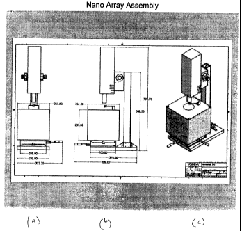
Figure 20 illustrates an engineering drawing for a nanoarray assembly.
Figure 21 illustrates an engineering drawing for a plate for use in mounting a
microscope.
Figure 22 illustrates an engineering drawing for a plate for use in a bottom
enclosure.
Figure 23 illustrates an engineering drawing for a plate for use in a top
enclosure.
Figure 24 illustrates an engineering drawing for a block for use in a pen
base.
Figure 25 illustrates an engineering drawing for a plate for use in a pen
base.
Figure 26 illustrates an engineering drawing for a disc for use in a pen
holder.
Figure 27 illustrates an engineering drawing for a lever for use in a pen
holder.
Figure 28 illustrates an engineering drawing for a plate for use in a pen
holder.
Figure 29 illustrates an engineering drawing for a base for use in an adapter.
Figure 30 illustrates an engineering drawing for a top piece for use in an
adapter.
Figure 31 illustrates another engineering drawing for a top piece for use in
an
adapter.
Figure 32 illustrates an engineering drawing for a base.
Figure 33 illustrates an engineering drawing for a cover for a rear enclosure.
Figure 34 illustrates an engineering drawing for a cover for a front
enclosure.
Figure 35 shows a photograph of the larger instrument or apparatus.
Figure 36 shows a photograph focusing on the multi-axis assembly.
Figure 37 shows a photograph focusing on the microscope and environmental
chamber.
Figure 38 shows a photograph focusing on the microscope and environmental
chamber from a top view.
Figure 39 shows a photograph focusing on the microscope without the
environmental chamber and showing pen holder and substrate.
Figure 40 is similar to Figure 39 but shows a side view.
Figure 41 shows an environmental chamber removed from the instrument.
Figure 42 shows instrument wiring.
Figure 43 shows a perspective view of the instrument.
6
CA 02681443 2009-09-21
WO 2008/141048 PCT/US2008/062959
Figure 44 shows a perspective view of the instrument.
Figure 45 shows inserting the environmental chamber onto the instrument.
Figure 46 shows inserting the environmental chamber onto the instrument.
DETAILED DESCRIPTION
INTRODUCTION
All references cited herein are incorporated by reference in their entirety.
To practice the presently claimed embodiments, one skilled in the art can use
as needed, for example:
(i) Fundamentals ofMicrofabrication, The Science of Miniaturization, 2nd Ed.,
Madou,
(ii) The Nanopositioning Book. Moving and Measuring to Better than a
Nanometre, T.R. Hicks et al, 2000;
For example, use of piezoelectric effects in microfabrication and MEMS is
known. See for example Madou at pages 551-560.
APPARATUS
Various important elements are described below. One skilled in the art can
utilize these elements using known hardware, software, controller, mountings,
cables, enclosures, electrical wiring, power supplies, and the like. In some
cases,
elements can be obtained as part of the materials and components obtained from
vendors and distributors.
The apparatus can be an instrument or a component to an instrument.
A part can be a single part or a plurality of components fabricated together
to
function as a single part. An assembly can be a plurality of components
fabricated
together to function as a single assembly.
MULTI-AXIS ASSEMBLY
Three-axis, five-axis, and six-axis assemblies are known in the art. The
apparatus can comprise at least one multi-axis assembly which can provide at
least
five modes of motion control via stages. The multi-axis assembly can be a five-
axis
7
CA 02681443 2009-09-21
WO 2008/141048 PCT/US2008/062959
assembly. The five stages can be integrated but can be independent stages and
function independently.
Three axes can be the X, Y, and Z motions or directions known in the art. For
example, the X and Y motions can provide lateral or linear motion in a plane
in two
orthogonal directions respectively via an X and Y stage, respectively. The Z
motion,
via a Z stage, can provide height raising and lowering with respect to the
plane for
the X and Y motions. In other words, a perpendicular motion can be provided by
a
Z stage.
Additional motions can provide for tilt in two orthogonal directions. For
example, the plane can be tilted by rotation around an X axis, or rotation
around a Y
axis.
The five or more stages can be integrated into a single functioning unit,
subject to control by one controller.
If desired, one or more additional stages can be provided and integrated to
provide six or more stages. For example, a rotational stage can be added as a
sixth
stage of the multi-axis assembly.
Positioning systems and stages are known in the art including nanopositioning
systems and stages and piezoelectric nanopositioning stages. See for example
products by Linos, Goettingen, Germany. These include for example manual
positioners including for example linear stages, XY stages, goniometer stages,
rotary
stages, vertical translation stages, tilting stages, prism stages, LUMINOS
nanopositioners, and actuating drive, measuring and micrometer screws. These
also
include for example motorized positioners including for example linear stages,
XY
stages, rotary stages, and accessories. These also include controllers. These
also
include piezo systems including piezo positioners and piezo controllers.
A nanopositioning stage can displace objects at a nanometer range.
Various methods of actuation and motion can be used including for example
piezoelectric, electrostatic, electromagnetic, and magnetostrictive.
Piezoelectric nanopositioning stages can comprise precision motors, including
piezoelectric motors, for motion control as known in the art. See for example
products and patents from Nanomotion Ltd (Yokneam, Israel). See for example US
Patent Nos. 7,211,929; 7,199,507; 7,183,690; 7,119,477; 7,075,211; 7,061,158;
8
CA 02681443 2009-09-21
WO 2008/141048 PCT/US2008/062959
6,979,936; 6,879,085; 6,747,391; 6,661,153; 6,617,759; 6,473,269; 6,384,515;
6,367,289; 6,247,338; 6,244,076; 6,193,199; 6,064,140 to Nanomotion. US Patent
No. 5,696,421 to Nanomotion describes multi-axis a rotation device including
orthogonal axes. Piezoelectric micromotors are described in for example US
Patent
No. 5,616,980.
See also Friend et al., IEEE Transactions on Ultrasonics, Ferroe%ctrics, and
Frequency Control, 53, 6, June 2006, 1160-1168.
Examples of electromagnetic include for example US Patent No. 7,185,590.
Electromagnetic components and positioners can be obtained from for example
Physik Instrumente. Examples of magnetostrictive include for example
components
available from Micromega Dynamics.
One skilled in the art can search vendors for nanopositioning technology,
devices, and components.
The multi-axis assembly can comprise a component such as a motor or a
stage adapted for linear X motion. For example, it can provide at least 10 mm,
or at
least 20 mm, or at least 40 mm of motion.
The multi-axis assembly can comprise a component such as a motor or a
stage adapted for linear Y motion. For example, it can provide at least about
10
mm, or at least about 20 mm, or at least about 40 mm of motion. A range can be
for example about 10 mm to about 60 mm.
The multi-axis assembly can comprise a component such as a motor or a
stage adapted for linear Z motion. For example, it can provide at least 10 mm,
or at
least 20 mm, or at least 40 mm of motion. A range can be for example about 10
mm to about 60 mm.
The range of motion in the X and Y plane can provide for example at least
about 400 square mm, or at least about 900 square mm, or at least about 1,600
square mm of coverage.
In some cases, a greater range of motion can be needed for the X motion and
the Y motion, compared to the Z motion. For example, range for Z motion may be
approximately 33% to 67% of the X motion range or Y motion range.
The multi-axis assembly can comprise a component such as a motor or a
stage or a goniometer adapted for a first tilting motion. For example, a tilt
angle
9
CA 02681443 2009-09-21
WO 2008/141048 PCT/US2008/062959
can be for example at least 2 degrees, or at least five degrees, or at least
10
degrees.
The multi-axis assembly can comprise a component such as a motor or a
stage or a goniometer adapted for a second tilting motion. This can function
independently of the first tilt. For example, a tilt angle can be for example
at least 2
degrees, or at least five degrees, or at least 10 degrees.
The tilting motions can provide alignment between the plane surface of the
substrate and the plane surface of the pen assembly. Moreover, the tilting
motions
can allow for better coating of material onto tips from a substrate, or better
delivery
or deposition of materials from the tip to the substrate. The angle between
the tip
and the substrate can be better controlled with multi-axis tilting. For
example, tilt
angles of about 7 degrees to about 15 degrees can be used as known in the art.
In particular, piezoelectric components and motors can be used effectively.
The multi-axis assembly can comprise one or more encoders including for
example optical encoders, which are integrated with other elements including
motors.
The multi-axis assembly can comprise multi-channel controllers and amplifiers
to drive piezomotors.
The stages can have a resolution of 5 nm and a repeatability of 15 nm or
even more preferably 5 nm. Operation travel speed can be for example at
least
100 nm/sec or at most 20 cm/sec and a range can be for example about 100
nm/sec
to about 20 cm/sec.
All five stages can be integrated into the multi-axis assembly and controlled
from a single multi-channel controller. This design can isolate the precision
mechanics from other parts of the system and can protect stages from operation
under specific conditions such as high humidity or temperature, which might be
applied during a fabrication process. Integrating all five stages can provide
more
room and flexibility for positioning components including for example pens,
inkwells,
dispersing system, environmental chamber, and optics. The multi-channel
controller
can be designed for parallel and independent operation of the stages and it
supports
reading, processing, and adjusting the position of each stage through its own
logical
processor.
CA 02681443 2009-09-21
WO 2008/141048 PCT/US2008/062959
The multi-axis assembly can be isolated from the working environment by an
expandable screen.
The individual stages can comprise metals such as aluminum or steel.
In one embodiment, a piezo-tube actuator can be integrated with the stages.
It can be installed on the uppermost stage.
The stages can be tuned, particularly when non-linear processes are used to
drive processes are present as in many piezoelectric motors. Stage performance
can
depend on parameters such as for example speed of translation, travel range,
and
stage load. Users can optimize PID parameters (proportional-integral-
derivative) for
short-range and long-range motions for each stage of the assembly. Users can
determine the correct PIDs and specify them in, for example, motion management
software.
The multiple stages can be integrated so that they function together. For
example, they can be placed on each other, including for example to make a
vertical
stack. For example, in one embodiment, the multi-axis assembly can be
assembled
so that the lowest stage is the Z stage; disposed on the Z stage is a first
tilt stage;
disposed on the first tilt stage is a second tilt stage; disposed on the
second tilt
stage is an X stage; and disposed on the X stage is a Y stage. The Z axis
stage can
be at the bottom and bear weight of other stages. One skilled in the art can
integrate the different stages to function together and independently. For
example,
the maker of or vendor for a particular nanopositioning device can engineer
how to
integrate that particular nanopositioning stage with other nanopositioning
stages to
satisfy the specifications needed.
The multi-axis assembly can be supported by an XY coarse translation stage.
This can be manually operated. It can provide, for example, a 50 mm X 50 mm
view
over the entire substrate area. The coarse translation stage can be relatively
large
and can have, for example, a base of at least 10 cm, or at least 20 cm.
Resolution
can be for example down to at least one micron. Coarse translations stages can
be
obtained via, for example, Linos, Goettingen, Germany. Examples include the X-
Y Stages XY 200 with Digital Micrometer.
In addition, software can be integrated to control and/or tune the motions of
the stages with nanometer resolution.
11
CA 02681443 2009-09-21
WO 2008/141048 PCT/US2008/062959
Working examples for the multi-axis assembly are described further below.
ENCLOSURE/CONTROLLER/ AND WIRING FOR MULTI-AXIS ASSEMBLY
The multi-axis assembly can be disposed in an enclosure or housing. This can
protect the precision mechanics from particulates, including dust. This can
also
separate the environment around the pen assembly and substrate from the
environment of the multi-axis assembly. The enclosure can be made of for
example
any solid structural element including metal or polymer (including plastic) or
ceramic. The enclosure can be adapted to not move despite motion of the multi-
axis
assembly. The enclosure can comprise a series of parts which function
together,
e.g., plates, including for example a top plate, a bottom plate, and one or
more side
plates. Supporting structures like rods can be used.
The top plate can have an opening. The opening can be adapted to function
with and be sealed by the table assembly when the table assembly is in, for
example, a lower position. The multi-axis assembly and the table assembly can
be
adapted so that there is physical separation and/or barrier between the
environment
of the enclosure and the environment of the environmental chamber. This can
also
keep out dust and debris from the multi-axis assembly. The opening can be also
sealed by for example a webbing of material secured to the table assembly and
the
top housing plate. Alternatively, a circular brush seal can be used. A plate
can be
used to allow the table assembly to move freely while being held flat to the
bottom
of the top housing plate. Hence, when the table assembly moves, so does the
plate
while still covering the opening. Discs can be used including combinations of
metal
and plastic discs.
The wiring of the multi-axis assembly can be carried out with use of cables.
For example, ten cables can be used, wherein for example five are for the
motors
and five are for the encoders.
The controller and amplifiers can be adapted by methods known in the art
and information supplied by vendors. Cables and wires can be used as known in
the
art. The size, flexibility, exit point, and length can be adapted for a
particular
application.
12
CA 02681443 2009-09-21
WO 2008/141048 PCT/US2008/062959
Working examples for the enclosure, controller, and wiring are described
further below.
TABLE ASSEMBLY/REMOVABLE SUBSTRATE
The apparatus and multi-axis assembly can further comprise a table
assembly, which can function as or be coupled with a sample holder or
substrate
holder. The table assembly can be adapted to hold and position a wide variety
of
substrates with different sizes and shapes. For example, the table assembly
can be
adapted to accept common commercial substrates up to for example 5 inches or
up
to 12 inches in length or diameter. The table assembly can be rotated and if
desired
locked into an arbitrary or chosen position.
The table assembly and substrate holder can be exchangeable. The table
assembly and substrate holder can be adapted for temperature adjustment and
control. For example, it can be equipped with a heater or cooler. The table
assembly and substrate holder can be moved and positioned to be aligned with
the
X and Y axes of the positioner.
A removable substrate can be controlled by the multi-axis assembly. The
substrate can be flat. The substrate can be adapted to couple with and be
positioned by the multi-axis assembly. The substrate can be moved in the X-
direction, the Y-direction, and the z-direction, as well as tilted in any of
the two
orthogonal tilt modes.
The substrate can be large enough to provide for macroscale positioning.
Substrates can be metal, ceramic, polymer, glass, composite, blend, or any
other
solid material. The substrate can be surface treated. For example, a thin
layer or
layers or a monolayer can be disposed on the substrate surface. An example is
a 1
inch X 3 inch slide such as a glass slide. The glass slide can be treated.
A working example of a table assembly is further described below.
VIEWING ASSEMBLY/MICROSCOPE
The apparatus can comprise a viewing assembly such as for example a
microscope, including an optical microscope or a combination of an optical and
fluorescent microscope. For fluorescence, an IR laser can be included. This
can be
13
CA 02681443 2009-09-21
WO 2008/141048 PCT/US2008/062959
used for visual monitoring of fabrication processes, including positioning and
alignment and making sure spotting has occurred. The optics can be
characterized
by high resolution and long working distance. For example, a working distance
(e.g., distance between objective lens and sample surface) of at least about
20 mm
or at least about 30 mm can be used, or about 30 mm to about 40 mm (e.g., 34
mm). An integrated zoom function can be used to adjust the field-of-view from
for
example about 2.1 X 2.8 mm to about 0.21 X 0.28 mm. These zoom values can
depend on the microscope specifications. The focus and zooming functions can
be
motorized and can be accessed from a remote controller or through computer
software. The resolution can be such to allow visualization of objects down
to, for
example, about 400 nm.
The images can be captured by video cameras and recorders and the like.
A microscope such as for example an A-Zoom2 10X Series analytical
microscope (10:1 zoom range) can be obtained for example from Qioptiq Imaging
Solutions, Rochester, NY. Optem objectives can be used.
A working example of the viewing assembly is described further below.
An important feature is the ability for detection of submicron features. For
example, dots can be generated over an array with dot diameter which decreases
to
less than one micron, but the dot can be detected with gray value measurements
as
a function of distance over the array. Detection can be achieve by, for
example,
fluorescent microscopy. Detection can also follow hybridization of arrays
including
submicron arrays.
PEN ASSEMBLY & DELIVERY
The pen assembly can be adapted to deliver material from a tip to a
substrate. The tip can be disposed on a cantilever. For example, a single tip
can be
used. Or a plurality of tips can be used. The tips can be disposed on an array
of
cantilevers, wherein each cantilever comprises one tip. For example, a one
dimensional array of tips can be used. Alternatively, a two dimensional array
of tips
can be used. See for example US patent application no. 11/690,738 and US
provisional application no. 60/894,657. A two dimensional array can comprise
for
example between about 10,000 pens to about 100,000 pens, such as about 55,000
14
CA 02681443 2009-09-21
WO 2008/141048 PCT/US2008/062959
pens. In one embodiment, a two dimensional 10X10 pen array can be built and
integrated with the rest of the instrument for, for example, high-throughput
printing
DNA and proteins.
MEMS fabrication methods can be used to prepare pen assemblies including
photolithography and electron beam lithography methods.
In particular, a nanoscale, sharp tip can be disposed on a cantilever
including
at the end of a cantilever. Tips can be nanoscale tips including for example
scanning probe microscope tips including atomic force microscope tips. Tips
can be
solid or can be solid but have an opening, channel, or aperture.
Tips can be made of hard inorganic materials, e.g., SiN, silicon, or can be
made of softer organic materials or can comprise coatings of harder or softer
materials. Tips can be adapted for delivery of materials. For example, tips
can be
longer than normally made for mere imaging. Tips can be curved. Tips can be
adapted to hold more material for delivery. Tips can be adapted to hold more
viscous materials like materials comprising polymers or DNA or protein. Tips
can
also as needed be adapted for imaging such as AFM imaging.
The pen assembly can be adapted to be stationary or movable. In particular,
it can be adapted to be movable in an X direction, a Y direction, or a Z
direction. Or
it can be adapted to be movable in only the Z direction. Here, the X direction
and Y
direction substantially are with respect to the plane of the substrate,
whereas the Z
direction is perpendicular to this plane.
The pen assembly can be moved and positioned to be aligned with the X and
Y axes of the positioner. The pen assembly can be adapted to flt into an
unmovable
bracket. The bracket can be adapted as needed to comprise and hold items such
as
microchips or preamplifiers within a few centimeters of the pens.
Methods and devices and instruments are known in the art for delivering or
depositing material from a tip or a pen to the substrate including at the
nanoscale.
See for example US Patent Nos. 6,635,311 and 6,827,979 to Mirkin et al (DPN
printing or DIP PEN NANOLITHOGRAPHY printing). See also for example US
Patent Publication 2005/0266149 to Henderson et al. The materials delivered
can be
for example organic, inorganic, or biological materials. Direct-write methods
can be
used. See for example Direct-Write Technologies for Rapid Prototyping
Applications,
CA 02681443 2009-09-21
WO 2008/141048 PCT/US2008/062959
Sensors, Electronics, and Integrated Power Sources, Ed. Pique, Chrisey, 2002,
including for example chapters 10 and 18. Actuated tips are known. See for
example US Patent No. 6,642,129 to Liu et al. Biological materials can be
deposited
including nucleic acid and protein or peptide materials. See for example US
Patent
Publication 2003/0068446 and PCT publication WO/2003/048314. Inks can be
based on DMF solutions of DNA. Sol gel materials can be deposited. See for
example US patent publication 2003/0162004. Polymers and conducting polymers
can be delivered. See for example US Patent Publication 2004/0008330 and US
Patent No. 7,102,656. Thermal delivery methods can be used. See for example US
patent publication 2006/0040057. Catalyst materials can be delivered. See for
example 2004/0101469 and US Patent No. 7,098,056. Conductive materials and
precursors thereof can be delivered. See for example 2004/0127025 and US
Patent
No. 7,005,378. Magnetic materials can be delivered. See for example
2004/0142106. Monomers can be delivered. See for example 2005/0272885.
The materials deposited on the surface can adsorb to, chemisorb to,
covalently bond to, or ionically bond to the surface. In many cases, a stable
deposition is desired.
One embodiment comprises delivery of compounds which form self-
assembled monolayers, such as sulfur compounds like thiols and sulfides
deposited
on gold.
One embodiment comprises deposition of antibodies, enzymes, and many
other types of proteinaceous or peptide compounds or materials.
One embodiment comprises deposition of RNA, DNA, nucleic acids,
oligonucleotides, and any other information containing monomer or polymer
founa in
RNA and DNA.
Nanomaterials can be deposited including nanoparticles, nanorods,
nanowires, nanotubes, fullerenes, dendrimers, and the like.
Material can be deposited, delivered, or patterned, and is then used to adsorb
or bind to additional materials, including for example proteins or nanowires
or other
small particles. See for example US Patent No. 7,182,996.
16
CA 02681443 2009-09-21
WO 2008/141048 PCT/US2008/062959
The material deposited on the substrate can be liquid, wet, dry, or solid.
Femtoliter amounts of inks can be deposited. Surfactants can be used. See for
example, US Patent Publication 2006/0242740.
Humidity, temperature, and other parameters can be adapted so that a
meniscus is formed between tip and substrate. Capillary forces and wetting
interactions can be controlled.
Alignment can be controlled by computer software. See for example
2003/0185967. Calibration can be controlled by computer software. See for
example US Patent No. 7,060,977.
Layered structures can be fabricated, and the height of structures can be
increased with multiple depositions. One layer can be deposited. Another layer
can
be deposited thereon.
Structures can be random or regular, continuous or discontinuous, dots or
lines, straight lines or curves lines, and the like.
Tips can be modified as desired. For example, tips can be coated with
polymer if desired. See for example 2005/0255237.
In one embodiment, laser optics can be used for positioning and feedback.
However, in another embodiment, the laser optics can be eliminated. For
example,
if the pen is adapted with sensors, then laser optics can be eliminated. This
can
simplify the device and allow for faster operation.
Structures can be formed which are nanometer in scale and separated by nm
ranges. These can be nanostructures. Lateral dimension can be for example a
line
width or a dot diameter. For example, lateral dimension can be about 5 microns
or
less, or about 1,000 nm or less, or about 500 nm or less, or about 250 nm or
less, or
about 100 nm or less. Lateral dimension can be for example at least about 1
nm, or
at least about 10 nm, or at least about 25 nm. Structures can be separated by
distances or average distances of for example about 5 microns or less, or
about
1,000 nm or less, or about 500 nm or less, or about 250 nm or less, or about
100
nm or less. This separation distance can be an edge to edge distance or a
center to
center distance.
17
CA 02681443 2009-09-21
WO 2008/141048 PCT/US2008/062959
Patterning can be done by delivery of different types of inks or materials.
For
example, at least two different materials, or at least twelve different
materials, can
be delivered onto a single substrate.
WO 2006/076302 (BioForce Nanosciences) describes surface patterning tools
and piezoelectric motion assemblies.
Working examples of pen assemblies are described further below.
ENVIRONMENTAL CHAMBER
The apparatus can further comprise an environmental chamber.
Environmental conditions can be controlled therein so they are independent of
the
surrounding air using a chamber that seals a volume between the multi-axis
assembly (which may be enclosed) and the optical microscope. The environmental
chamber can be adapted to enclose the pen assembly and substrate. The chamber
can be transparent. It can be a plastic or glass for example. Because the
chamber
is relatively small, parameters such as temperature, humidity, and gas
composition
can be easily controlled. The chamber can be adapted for incoming air or gas
streams and outlets for temperature and humidity sensors. In particular, these
parameters can be controlled to control the delivery or deposition of material
from
tip to substrate. The environmental chamber can also be integrated with
software to
provide automatic feedback control. The environmental chamber can be equipped
with electronic temperature and humidity sensors to provide automatic feedback
control.
The working examples below further describe an example of an
environmental chamber.
ADDITIONAL PARAMETERS, HARDWARE, AND SOFTWARE
Methods and devices known in the art can be used to protect the instrument
or apparatus from vibration. For example, the apparatus can be disposed,
placed,
and used on an air table.
Frames can be built and integrated with the rest of the instrument to mount
two dimensional pen arrays and facilitate in plane (2D) alignment.
18
CA 02681443 2009-09-21
WO 2008/141048 PCT/US2008/062959
In addition, a system can be built and integrated to rotate pen arrays with
respect to sample structures with, for example, 0.001 degree resolution.
Software can be used to manage delivery of material from pen assembly to
substrate as known in the art. See for example products from NanoInk, Skokie,
IL
and US Patent No. 6,827,979.
Known computer hardware or instrument hardware in general can be
integrated with software and functioning as controller. For example, a laser-
based
feedback system can be combined with software, or function independently of
the
software, as controller to provide automated operation, including approach,
alignment, inking, and printing, and to improve quality of printing.
In some embodiments, atomic resolution scanners can be added to the
instrument to provide independent imaging modality with sub-nanometer spatial
resolution and/or registration. These scanners and the tips in the assembly
used for
inking and writing, can together provide simultaneous patterning and imaging
of
nanoscale features.
Kits can be used. For example, these can comprise accessories such as for
example substrates, ink materials, pens, instructions, containers, inkwells,
and the
like.
Examples of instrument features which can be controlled by software include:
1. execution of stage routines from a motion control panel;
2. allow incremental and continuous motions;
3. allow low and high speed motions;
4. enable/disable stages;
5. specifly and execute target positions;
6. monitor current positions for all stages;
7. execute stage routines for all stages simultaneously;
8. capture, save, and execute selected positions;
9. run routine to define top surface of print substrate that allows automatic
approach and print capabilities;
10. calculate approach positions within printing region;
11. allows aligning for one dimensional and two dimensional pen arrays;
12. capture, save, and execute inking positions;
19
CA 02681443 2009-09-21
WO 2008/141048 PCT/US2008/062959
13. specify limits for safe moves;
14. approach and withdraw pens from motion control panel and through a pattern
configuration code;
15. save and open experimental settings;
16. specify pattern configuration and print parameters (such as number,
spacing,
speed, length, and dwell time, for example) for individual dots and lines, and
their
arrays;
17. execute multiple patterns with specific print parameters in a single run;
18. allows re-inking pens during print runs; and
19. monitor status and remaining time of the print process.
In one embodiment, a main window can be built into the software which can
provide imaging, further menu bars, icons to activate functions, data entry
sections,
and information read-out sections.
In one embodiment, for example, software can be prepared and used which
provides for two categories of operation: (i) motion control, and (ii) array
configuration. For example, the motion control software can be used to access
frequently used routines, including for example pre-tuned stage displacement
and
specified locations. In addition, array configuration software can be used to
specify
individual dots and lines and arrays of dots and lines.
The software main window can provide, for example, a menu bar with options
including project, configure, pattern, window, and help options. The main
window
can show current positions and target positions for the pen and the x, y, z,
and Tx,
and Ty tilt positions. The main window can also show, for example, approach
calculations and inkwell information.
Under a project option, for example, information can be entered and accessed
which is project information related to, for example, date and time, sample,
ink(s),
writing tool, writing conditions, pattern configurations, and pattern
location.
Under a configure option, for example, one can set safe motion parameters
such as for example minimum and maximum travel distances for each axis.
Under a pattern option, for example, one can open a window to specify dot
and line features and their array configuration. Parameters include, for
example, the
number of arrays and number of elements within an array, spacing between the
CA 02681443 2009-09-21
WO 2008/141048 PCT/US2008/062959
arrays and the elements in X and Y directions, position of the first array and
first
element taking into account that positive values in the spacing tab can result
in
printing features bottom up left to right and vice versa.
Other pattern parameters can be controlled by software.
For example, arrays can be generated with information entry for number of
arrays, spacing, and origin. Here, a "repeat" parameter can control the number
of
times the array or element is to be repeated after the first complete run. For
example, for a pattern containing five arrays of 100 dots repeat "2" in the
array field
can mean that after all five arrays are completed they will be repeated two
more
times.
For drawing dots, one can enter information, for example, for number of dots,
spacing, and origin. A "dwell time" parameter can mean, for a dot generation,
how
long the writing pen remains in contact with sample surface to deposit ink or
molecules.
For drawing lines in the X and Y directions, one can enter information for
number of lines, spacing, and origin. One also can set a "line length" which
can bP
the same for both axes. One can also set speed of writing.
A "speed" parameter, controlled by software, can be the rate of pen
movement over the substrate surface to build a line.
A motion control panel can include the following exemplary features for a
manual operation of the stages: a plurality, for example nine, fixed motion
increments (in for example microns, e.g., one micron or five microns or 100
microns,
and a low speed (LS) setting, motion controls (check box, motion arrows, start
button, feedback position) per each stage. Motion increment buttons can be
used to
apply selected travel to all stages. The active motion increment can be
highlighted.
By pressing, for example, a key such as "<" or ">" arrows the related stage
can
execute the displacement. For each axis and for each motion increment, there
can
be optimized PID settings determined during the tuning process. Technically,
by
pressing the increment buttons, the related PID settings can be loaded to the
controller. PID settings can be stored in an ACS file that can have, for
example, a
plurality of buffers such as ten buffers. Each buffer can contain information
about
PID setting for a particular motion. Desired PIDs can be loaded by running the
21
CA 02681443 2009-09-21
WO 2008/141048 PCT/US2008/062959
related buffer. Each motion can have a letter indicating the axis, a square
box to
check or uncheck the axis, motion arrows to choose motion direction and a tab
presenting absolute coordinates of the stage (the feedback). In addition to
incremental motions, one can generate continuous motion by holding the arrows.
Also, for very precise positioning one can type particular coordinates into
the
position box on the right side and then press a Start button to execute the
motion.
A commercial motion control panel can be adapted for particular
configurations.
In a Layout panel section, the current position of the stages can be saved at
any time by pressing one of the buttons in the Layout panel and then pushing a
"'Capture" button. To execute a saved position, it can be enough to press the
related button and then "Go To" button. There can be for example ten available
buttons on a Layout panel. The first three, P1, P2, and P3 for example, can be
used
only to define the sample plane that is part of a procedure to calculate
Approach set
points. Other buttons can be used to save positions of one or more inkwells.
Other
buttons can be used for any position.
In an Approach button section, each sample such as a glass slide or a custom
substrate, can have specific Z and T values. One can define the top plane of
the
sample in order to calculate approach points for any X/Y position. To do that
a user
can manually approach the substrate surface at three different locations which
define a plane. Another way to do this is to start at the most negative X and
Y
values, then to keep Y constant, and move to the most positive X, and finally
move
to the most positive Y.
These three points typically occur at corners of a rectangular substrate. At
each position (e.g., P1, P2, and P3), the X, Y, and Z are acquired by pressing
a
Capture button on the Layout panel. The coordinates of the three points are
used to
define a plane using the three points plane equation. Upon pressing the
Calculate
button, the equation of the plane will be solved for Z as a function of X and
Y. Now,
when the Approach button is pressed, the application will use the derived
equation
to calculate Z for any particular X and Y. By pressing the Approach button,
the
program algorithm can read X and Y coordinates, then put them into the
equation to
calculate the particular Z, and finally execute the desired Z motion. Hence,
one
22
CA 02681443 2009-09-21
WO 2008/141048 PCT/US2008/062959
embodiment provides that the controller comprises software to enable
definition of
the substrate plane.
APPLICATIONS
The instrument and apparatuses described herein can be used in a wide
variety of applications.
In some applications, material is deposited onto the surface which has not yet
been patterned. In other applications, material is deposited onto the surface,
wherein the surface comprises a defect in need of repair. For example,
additive
repair can be carried out. The surface can be pretreated or indexed as needed
for a
particular application. Surfaces can be rendered hydrophilic or hydrophobic,
and
roughness can be controlled.
One application is in the fabrication of electronic circuits based on
combinations of insulative, semiconductive, and conductive features.
Electronic
parameters can be measured. See for example 2004/0026681.
One application is in photomask repair. See for example 2004/0175631.
One application is in flat panel display repair. See for example
2005/0235869.
Fabricated surfaces can be further subjected to etching, wherein the materials
deposited onto the surface act as etch resists. See for example 2006/0014001.
Nanoscale testing can be carried out as described in for example 7,199,305.
One particularly important application is in the fleld of bioarrays or
microarrays or nanoarrays including protein arrays and DNA arrays. See for
example
Microarrays, Muller, Roder, 2006; Microarrays foran Integrative Genomics,
Kohane,
2003. The arrays fabricated as described herein can be further analyzed by
fluorescent and scanning probe methods including AFM methods. For example,
diagnostics can be done with these arrays. Additional description for
bioarrays can
be found in for example US Patent No. 6,573,369.
Arrays can be based on dots or lines. One particularly important embodiment
comprises arrays of oligonucleotides and cDNA. For example, oligonucleotides
can
have for example 5 mers to 60 mers. The oligonucleotides can be modified or
adapted at the terminal position for chemisorption or covalent bonding to the
23
CA 02681443 2009-09-21
WO 2008/141048 PCT/US2008/062959
substrate surface. Other compounds for inks in patterning on surfaces can be
based
on, for example, 2 mers to 150 mers.
Oligonucleotide hybridization assays can be carried out . Examples include
HIV, VV, BA, and EV hybridized arrays.
When arrays are made, AFM phase images of the arrays can be carried out
showing shape and size consistency within the array. For example, the feature
size
canbe210f5nm.
One aspect of this technology is delivery of ink to places where it can be
used
including for example microfluidics and inkwells and reservoirs. See for
example
2005/0035983 and US Patent No. 7,034,854.
Arrays can be periodic or non-periodic.
The instrument can be used as a plotter and can be used to draw a wide
variety of shapes including continuous lines and dots.
Force feedback can be used as desired.
Software can be integrated with the instrument to automate the operation
and/or to improve the quality of the printing results.
Presynthesized molecules can be spotted.
Nanoassemblies can be built by integrating molecules into prefabricated
MEMS.
Layer-by-layer growth can be achieved by sequential deposition of solutions.
Solid phase synthesis can be carried out. One example is in situ molecular
synthesis via multiplexed ink delivery. Another example is making templates
for
further molecular assembly through chemical synthesis. Another example is
ordered
supramolecular assemblies based on coordination chemistry.
WORKING EMBODIMENT/EXAMPLE
Non-limiting working example is described. As an example of a multi-axis
assembly, a 5-axis assembly instrument was built based on the following non-
limiting specifications for the multi-axis assembly comprising five stages of
independent motion:
The XY travel is at least 40 mm in X direction and Y direction.
24
CA 02681443 2009-09-21
WO 2008/141048 PCT/US2008/062959
The Z travel is at least 20 mm.
The tip/tilt travel is at least 10 degrees.
Position feedback is provided by precision linear encoders with 5 nm
resolution.
Actual linear resolution for X, Y, and Z motions is at least 15 nm and at
least 15
nm for repeatability.
The angular resolution is at least 0.001 degree.
The lowest guaranteed travel speed is at least 100 nm/sec.
The highest travel speed is at most 1-10 mm/sec.
A vendor can be used to fabricate the multi-axis assembly within these
specifications. One vendor, for example, is NanoMotion, Ltd. (Yokneam, Israel;
a
)ohnson Electric Co.). Alternatively, one can refer to other vendors in
nanopositioning technology or to the technical literature on how to assemble a
multi-
axis assembly.
Figures 1(a)-(c) illustrate the larger instrument including the microscope and
enclosure for the multi-axis assembly. See also Figure 20.
Figure 2 illustrates an embodiment for the microscope showing the
microscope, microscope mount plate, and U-channel braces, as well as cross
braces.
This design provides strength and saves weight. It allows cables to be run
down the
center of the channels and exit out the side of the U-channel (not shown).
Figure
21 illustrates one example of a microscope mount plate.
Figure 3 shows an embodiment for an assembly for mounting the pen array.
The pen array can be glued to this assembly. The assembly can comprise a block
for a pen base as illustrated in for example Figure 24. The assembly can
further
comprise a plate for the pen base as illustrated in for example Figure 25. The
assembly can further comprise a disk for a pen holder as illustrated in for
example
Figure 26. The assembly can further comprise a lever as illustrated in for
example
Figure 27. The assembly can further comprise a plate for the pen holder as
shown
in for example Figure 28.
Figure 4 shows a table assembly for mounting on top of the multi-axis
assembly. The top part of the assembly can be either left floating to allow
for
rotational adjustment, or a bolt can be put in place for a solid connection. A
CA 02681443 2009-09-21
WO 2008/141048 PCT/US2008/062959
substrate can be put on this table assembly. The bottom part can be fabricated
as
shown in for example Figure 29. The top part can be fabricated as shown in for
example Figures 30 and 31.
Figure 5 shows an enclosure assembly for the multi-axis assembly. The
enclosure comprises four square rods, a top plate, a bottom plate, two sheet
metal
sides. The bottom plate can comprise an extrusion so that the enclosure can
sit on
an XY table. This option allows the enclosure to be rotated if required. Or
the
enclosure can be secured to the XY table for a solid mount. Figure 22 further
illustrates an example of a bottom plate. Figure 23 further illustrates an
example of
a top plate. Figure 33 illustrates an example of a rear enclosure. Figure 34
illustrates an example of a front enclosure.
Figure 6 shows an environmental chamber which can allow control of for
example temperature, humidity, and flow of gasses other than the surrounding
room's atmosphere.
MOTION STUDY
Figures 7-13 illustrate the multi-axis motion step-by-step.
In Figure 7, the multi-axis assembly is shown at its lowest position. The pens
are not in contact with the substrate which would sit on top of the table
assembly.
26
CA 02681443 2009-09-21
WO 2008/141048 PCT/US2008/062959
In Figure 8, the Z-axis stage elevates the table assembly and substrate,
although it is not yet in contract with the pen.
In Figure 9, the Z-axis stage has not elevated the table assembly and
substrate sufficiently that the pen is now in contact with the substrate.
In Figure 10, the table assembly and substrate are tilted at five degrees by a
second stage.
In Figure 11, the table assembly and substrate are tilted again at five
degrees
by a second stage, wherein the tilt is orthogonal to the tilt of the Figure 10
tilt.
In Figure 12, the table assembly and substrate are moved by a fourth stage
20 mm.
In Figure 13, the table assembly and substrate are moved by a fifth stage
another 20 mm, wherein the move is orthogonal to the movement of Figure 12.
Figure 14 shows the top view of the top plate at most extreme position.
Figure 15 illustrates a top view of the top plate at lowest position. Here,
for
example, the table can sit into a 2 mm recess to create a seal with the top
plate.
The table can function therefore as a cover which can help prevent foreign
objects
from falling into the housing.
Figure 16 illustrates microscope mount designs.
Figure 17 illustrates an ACS controller and an AB2 Driver Box Front panel.
Figure 18 illustrates a Renishaw .1 micron resolution RGH encoder.
Figure 19 illustrates a Mercury TM3500 Smart Encoder Systems.
Figures 35-46 provide additional perspective photographs of a working model.
In Figures 35-36 and 43-44, the side panels of the enclosure for the multi-
axis
assembly are removed to allow viewing of the multi-axis assembly in a working
model.
Figures 37-38 shows the environmental chamber including a hole or view port
for viewing by the microscope in a working model.
In Figures 39-40, the environmental chamber is removed to better show the
pen assembly and the table assembly and substrate on the table assembly in a
working model.
Figure 41 shows the environmental chamber removed from the instrument in
a working model.
27
CA 02681443 2009-09-21
WO 2008/141048 PCT/US2008/062959
Figure 42 shows wiring in a working model.
Figures 45 and 46 show insertion of the environmental chamber in a working
model.
While the working model illustrates one or more embodiments, other
embodiments different than the working model can be within the scope of the
claimed inventions.
28