Note: Descriptions are shown in the official language in which they were submitted.
CA 02681665 2009-09-22
WO 2008/118352 PCT/US2008/003727
A STEP CARD AND METHOD FOR MAKING A STEP CARD
FIELD OF INVENTION
[0001] The present invention relates generally to the field of electronic
devices and,
more particularly, to the field of electronic cards with embedded powered
circuits and
the method of making such electronic cards.
BACKGROUND
[0002] The following description of the background of the invention is
provided
simply as an aid in understanding the invention and is not admitted to
describe or
constitute prior art to the invention.
[0003] Generally, electronic devices can be encapsulated in various materials
and
used for applications such as smart caTds or tags. Smart cards/tags may be
used as
credit cards, bankcards, ID cards, telephone cards, security cards or similar
devices.
Smart cards/tags are generally constructed by assembling several layers of
plastic
sheets in a sandwich array. Further, smart cards/tags contain embedded
electronic
components that enable the smart card to perform a number of functions.
[0004] European Patent 0 350 179 discloses a smart card wherein electronic
circuitry is encapsulated in a layer of plastic material that is introduced
between the
card's two surface layers. The method further comprises abutting a high
tensile
strength holding member against a side of a mould, locating the smart card's
electronic components with respect to that side and then injecting a reaction
moldable
polymeric material into the mould such that it encapsulates the electronic
components.
[0005] European Patent Application 95400365.3 teaches a method for making
contact-less smart cards. The method employs a rigid frame to position and fix
an
electronic module in a void space between an upper thermoplastic sheet and a
lower
thermoplastic sheet. After the frame is mechanically affixed to the lower
thermoplastic sheet, the void space is filled with a polymerizable resin
material.
-1-
CA 02681665 2009-09-22
WO 2008/118352 PCT/US2008/003727
[0006] U.S. Patent No. 5,399,847 teaches a credit card that is comprised of
three
layers, namely, a first outer layer, a second outer layer and an intermediate
layer. The
intermediate layer is formed by injection of a thermoplastic binding material
that
encases the smart card's electronic elements (e.g., an IC chip and an antenna)
in the
intermediate layer material. The binding material is preferably made up of a
blend of
copolyamides or a glue having two or more chemically reactive components that
harden upon contact with air. The outer layers of this smart card can be made
up of
various polymeric materials such as polyvinyl chloride or polyurethane.
[0007] U.S. Patent No. 5,417,905 teaches a method for manufacturing plastic
credit
cards wherein a mold tool comprised of two shells is closed to define a cavity
for
producing such cards. A label or image support is placed in each mold shell.
The
mold shells are then brought together and a thermoplastic material injected
into the
mold to form the card. The inflowing plastic forces the labels or image
supports
against the respective mold faces.
[0008] U.S. Patent No. 5,510,074 teaches a method of manufacturing smart cards
having a card body with substantially parallel major sides, a support member
with a
graphic element on at least one side, and an electronic module comprising a
contact
array that is fixed to a chip. The manufacturing method generally comprises
the steps
of: (1) placing the support member in a mold that defines the volume and shape
of the
card; (2) holding the support member against a first main wall of the mold;
(3)
injecting a thermoplastic material into the volume defmed by the hollow space
in
order to fill that portion of the volume that is not occupied by the support
member;
and (4) inserting an electronic module at an appropriate position in the
thermoplastic
material before the injected material has the opportunity to completely
solidify.
[0009] U.S. Patent No. 4,339,407 discloses an electronic circuit encapsulation
device in the form of a carrier having walls that have a specific arrangement
of lands,
grooves and bosses in combination with specific orifices. The mold's wall
sections
hold a circuit assembly in a given alignment. The walls of the carrier are
made of a
slightly flexible material in order to facilitate insertion of the smart
card's electronic
circuitry. The carrier is capable of being inserted into an outer mold. This
causes the
-2-
CA 02681665 2009-09-22
WO 2008/118352 PCT/US2008/003727
carrier walls to move toward one another in order to hold the components
securely in
alignment during the injection of the thennoplastic material. The outside of
the walls
of the carrier has projections that serve to mate with detents on the walls of
the mold
in order to locate and fix the carrier within the mold. The mold also has
holes to
permit the escape of trapped gases.
[0010] U.S. Patent No. 5,350,553 teaches a method of producing a decorative
pattern on, and placing an electronic circuit in, a plastic card in an
injection molding
machine. The method comprises the steps of: (a) introducing and positioning a
film
(e.g., a film bearing a decorative pattern), over an open mold cavity in the
injection
molding machine; (b) closing the mold cavity so that the film is fixed and
clamped in
position therein; (c) inserting an electronic circuit chip through an aperture
in the
mold into the mold cavity in order to position the chip in the cavity; (d)
injecting a
thermoplastic support composition into the mold cavity to form a unified card;
and (e)
thereafter, removing any excess material, opening the mold cavity and removing
the
card.
100111 U.S. Patent No. 4,961,893 teaches a smart card whose main feature is a
support element that supports an integrated circuit chip. The support element
is used
for positioning the chip inside a mold cavity. The card body is formed by
injecting a
plastic material into the cavity so that the chip is entirely embedded in the
plastic
material. In some embodiments, the edge regions of the support are clamped
between
the load bearing surfaces of the respective molds. The support element may be
a film
that is peeled off the finished card or it may be a sheet that remains as an
integral part
of the card. If the support element is a peel-off film, then any graphics
elements
contained therein are transferred and remain visible on the card. If the
support
element remains as an integral part of the card, then such graphics elements
are
formed on a face thereof and, hence, are visible to the card user.
100121 U.S. Patent No. 5,498,388 teaches a smart card device that includes a
card
board having a through opening. A semiconductor module is mounted onto this
opening. A resin is injected into the opening so that a resin molding is
formed under
such condition that only an electrode terminal face for external connection of
said
-3-
CA 02681665 2009-09-22
WO 2008/118352 PCT/US2008/003727
semiconductor module is exposed. The card is completed by mounting a card
board
having a through opening onto a lower mold of two opposing molding dies,
mounting
a semiconductor module onto the opening of said card board, tightening an
upper die
that has a gate leading onto a lower die and injecting a resin into the
opening via the
gate.
[0013] U.S. Patent No. 5,423,705 teaches a disc having a disc body made of a
thermoplastic injection molded material and a laminate layer that is
integrally joined
to a disc body. The laminate layer includes an outer clear lamina and an inner
white
and opaque lamina. An imaging material is sandwiched between these lamina.
[0014] U.S. Patent No. 6,025,054 discloses a method for constructing a smart
card
using low shrinkage glue to hold the electronic devices in place during the
devices
immersion in thermosetting material that becomes the core layer of the smart
card.
The method disclosed in U.S. Patent 6,025,054 has considerable drawbacks.
Primarily, the disclosed method produces warping and other undesirable
physical
defects caused by the curing of thermosetting material. Further, this method
is
suitable only for cards having one or two components, thus limiting its
functionality.
In addition, the method disclosed in U.S. Patent 6,025,054 creates defects
such as
voids and air bubbles within a smart card because the geometric shapes of the
electronic components within the card obstruct the flow of the thermosetting
material
such that the thermosetting material flows around the components faster than
the air
can be pushed out of the core of the smart card. Moreover, U.S. Patent `054
requires
the use of custom equipment, significantly limiting the scope and scalability
of its
application.
[0015] Generally, electronic devices such as electronic cards are designed to
conform with known industry standards as well aesthetic appearance standards.
For
example, most if not all electronic cards are designed to be thin and
uniformly flat in
shape. The shape of these cards requires that any power source embedded in the
card
also have a small footprint. These smaller power sources have a limited power
capacity which in turn limits the life span of the electronic card. Moreover,
the types
of slimmer power sources available is small in number, which considerably
reduces
-4-
CA 02681665 2009-09-22
WO 2008/118352 PCT/US2008/003727
design choices for manufacturers. Accordingly, the above mentioned limitations
restrict more power intensive applications from being introduced in the
electronic
card market place. In view of the following, there is a need for a device and
a method
of constructing an electronic card that is capable of housing a number of
powered
electrical components without significantly increasing the size of the
electronic card
and its aesthetic design.
SUMMARY
100161 According to one embodiment, an electronic card includes a printed
circuit
board, having a top surface and a bottom surface; a plurality of circuit
components
attached to the top surface of the printed circuit board, wherein the circuit
components
positioned in a first portion of the electronic card are greater in height
than the circuit
components positioned in a second portion of the electronic card; a bottom
overlay
attached to the bottom surface of the printed circuit board; a top overlay
positioned
above the top surface of the printed circuit board; and a core layer
positioned between
the top surface of the printed circuit board and the top overlay, wherein the
first
portion of the electronic card has a greater thickness than the second portion
of the
electronic card.
[0017] According to another embodiment, a method for manufacturing an
electronic
card includes the steps of providing a printed circuit board having a top
surface and a
bottom surface; affixing a plurality of circuit components onto the top
surface of the
printed circuit board, wherein the circuit components positioned in a first
portion of
the electronic card are greater in height than the circuit components
positioned in a
second portion of the electronic card; affixing the bottom surface of the
printed circuit
board to a bottom overlay using a pressure sensitive adhesive tape or a spray-
on
adhesive; loading the printed circuit board and bottom overlay into an
injection
molding apparatus; loading a top overlay positioned above a top surface of the
printed
circuit board into the injection molding apparatus; injecting thermosetting
polymeric
material between the top surface of the printed circuit board, the plurality
of circuit
-5-
CA 02681665 2009-09-22
WO 2008/118352 PCT/US2008/003727
components and the top overlay such that the first portion of the electronic
card has a
greater thickness than the second portion of the electronic card.
BRIEF DESCRIPTION OF THE DRAWINGS
[0018] These and other features, aspects and advantages of the present
invention
will become apparent from the following description, appended claims, and the
accompanying exemplary embodiments shown in the drawings, which are briefly
described below.
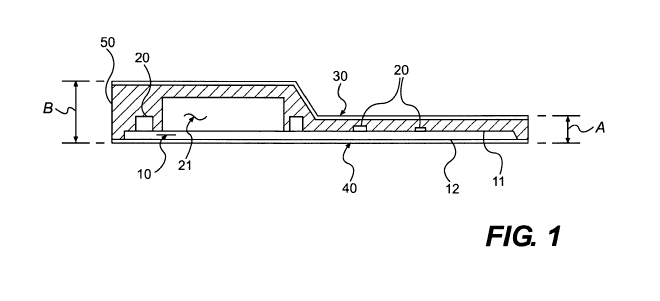
[0019] FIG. 1 is a sectional view of an electronic card according to one
embodiment
of the present invention.
[0020] FIG. 2 is a top sectional view of an electronic card according to one
embodiment of the present invention.
[0021] FIG. 3 is a sectional view of an electronic card and an injection
nozzle
according to one embodiment of the present invention.
[0022] FIG. 4 is a top sectional view of a series of electronic cards formed
on one
molded sheet according to one embodiment of the present invention.
DETAILED DESCRIPTION
[0023] Embodiments of the present invention will be described below with
reference to the accompanying drawings. It should be understood that the
following
description is intended to describe exemplary embodiments of the invention,
and not
to limit the invention.
[0024] According to one embodiment of the present invention, as shown in FIG.
1,
an electronic card 1 comprises a printed circuit board 10, a plurality of
circuit
components 20, a power source such as a battery 21, a bottom overlay 30, a top
overlay 40 and a core layer 50. The electronic card 1 has at least two
portions of
different thicknesses. The battery 21 is positioned in a first portion of the
electronic
-6-
CA 02681665 2009-09-22
WO 2008/118352 PCT/US2008/003727
card I having a thickness B. A second portion of the electronic card 1 has a
thickness
A. As shown in FIG. 1, the first portion (encapsulating the battery) has a
greater
thickness (B>A) than the second portion. The electronic card 1 may be used in
such
applications as smart cards, tags and/or wristbands.
[0025] The printed circuit board 10 has a top surface 11 and a bottom surface
12.
According to one embodiment of the invention, the printed circuit board 10 is
double-
sided. Accordingly, the printed circuit board 10 is configured to accommodate
a
plurality of circuit traces 14 (shown in FIG. 2) on the top surface 11 and on
the
bottom surface 12. The circuit traces 14 are configured to operably connect
the
plurality of circuit components 20 affixed to the printed circuit board 10.
The circuit
traces 14 electrically connect to the plurality of circuit components 20 such
that the
circuit components are capable of performing electrical functions within the
electronic
card 1.
[0026] The circuit traces 14 may be provided upon the surfaces 11, 12 of the
printed
circuit board in numerous ways. For example, the circuit traces 14 may be
formed on
the printed circuit board 10 with conductive ink. In the alternative, circuit
traces 14
may be etched onto the printed circuit board.
[0027] The printed circuit board 10 is comprised of any known conventional
material suitable for receiving an electronic circuit. For example, the
printed circuit
board 10 may be comprised of a flame retardant laminate with a woven glass
reinforced epoxy resin. This material is also known as FR-4 board.
Alternatively, the
printed circuit board 10 may be comprised of a plastic compound that is
suitable for
receiving conductive ink.
[0028] As shown in FIG. 1, and described below, the printed circuit board 10
is
configured to receive and vertically stabilize a plurality of circuit
components 20.
The plurality of circuit components 20 may be attached to the printed circuit
board 10
and specifically to the circuit traces 14 by any one of a number of methods.
For
example, in one embodiment of the invention, the circuit components 20 are
connected to the printed circuit board 10 with a conductive adhesive.
Preferably, the
-7-
CA 02681665 2009-09-22
WO 2008/118352 PCT/US2008/003727
plurality of circuit components are soldered onto the printed circuit board
10. The
plurality of circuit components 20 can be positioned anywhere on the printed
circuit
board 10 as desired. The purpose of the electronic card 1 and design
parameters will
dictate the position of the circuit traces 14 and the position of the circuit
components
20. Functionality will also dictate what types of circuit components 20
populate the
printed circuit board 10.
[0029] For example purposes only, the plurality of circuit components 20 could
be
one of a battery, a button, a microprocessor chip or a speaker. Any one or all
of these
circuit components could populate the printed circuit board 10 along any
portion of
the electronic card. Further, additional circuit components 20 may include but
are not
limited to LEDs, flexible displays, RFID antennas and emulators. Referring to
FIG.
2, a circuit layout for an electronic card 1 is shown. The printed circuit
board 10
shown in FIG. 2 is populated by a battery 21, a microprocessor 22 and a button
23. In
another embodiment of the present invention as shown in FIG. 2, the electronic
card 1
includes a liquid crystal display 24 as the circuit component 20 connected to
the
button 23. The liquid crystal display 24 may be used to display information to
a user,
such as an account balance. In the alternative or in addition to, the embedded
electronic card 1 shown in FIG. 2 may include a speaker (not shown).
[0030] Generally, the components shown in FIGS. 1 and 2 may vary in thickness
and length. For example, the electronic card 1 can have an overall thickness
of less
than 0.09 inches. A first portion of the electronic card can have a thickness
in the
range of .030 to .090 inches. The thickness of the first portion of the
electronic card
allows for larger, taller and more powerful power sources such as batteries 21
and to
be used in the electronic card 1. A second portion of the card can have a
thickness of
.030 inches or less. The variation in thickness of the first portion and
second portion
allows a more powerful card to be used with conventional applications that
were
originally design for cards of a smaller thickness. Accordingly, these
dimensions
allow the electronic card 1 to be compatible with the conventional equipment.
For
example purposes only, the battery 21 can have a thickness of .016 inches, the
push
button 23 can have a thickness of .020 inches and the microprocessor 22 can
have a
-8-
CA 02681665 2009-09-22
WO 2008/118352 PCT/US2008/003727
thickness of .015 inches. In addition, the electronic card 1 shown in FIG. 2
can have a
speaker (not shown) having a thickness of .010 inches.
[0031] As shown in FIG. 1, a bottom overlay 30 is attached to the bottom
surface 12
of the printed circuit board 10. The bottom overlay 30 can be, for example,
0.00 1 to
0.002 inches thick. The bottom overlay 30 can be attached to the printed
circuit
board 10 by any number of known methods. Preferably, the bottom surface 12 is
attached to the bottom overlay 30 using a pressure sensitive adhesive tape or
a spray-
on adhesive. The bottom overlay 30 may be comprised of any suitable material
but
preferably, the bottom overlay 30 is comprised of polyvinyl chloride (PVC) ,
polyester, acrylonitrile-butadiene-styrene (ABS), polycarbonate, polyethylene
terephthalate (PET), PETG, or any other suitable material.
[0032] According to one embodiment of the invention, the surface of the bottom
overlay 30 in contact with the printed circuit board 10 has printed
information.
Alternarively, printed information may be placed on the outside surface of the
bottom
overlay 30. For example, the bottom overlay 30 may include printed information
consistent with a standard credit card or identification tag, including a
name,
expiration date and account number. According to another embodiment of the
invention, the bottom overlay 30 may be clear or 2/5 clear/white printed.
Specifically,
a .002 inch thick piece of clear PVC material is laminated on to a layer of
white PVC
that is .005 inches in thickness.
[0033] A top overlay 40 positioned above the top surface of the printed
circuit board
is shown in FIG 1. The top overlay 40 may be comprised of any suitable
material,
for example, the top overlay 40 may be comprised of polyvinyl chloride (PVC) ,
polyester, acrylonitrile-butadiene-styrene (ABS), polycarbonate, polyethylene
terephthalate (PET), PETG, or any other suitable material. Like the bottom
overlay
30, the top overlay 40 can be, for example, 0.001 to 0.002 inches thick.
[0034] Alternatively, the outside surface of the top overlay 40 may have
printed
information. For example, the top overlay 40 may include printed information
consistent with a standard credit card or identification tag, including a
name,
-9-
CA 02681665 2009-09-22
WO 2008/118352 PCT/US2008/003727
expiration date and account number. According to another embodiment of the
invention, the top overlay 40 may be clear or "2/5 clear/white printed."
[0035] As previously mentioned, the overall thickness of the electronic card
can vary
as well as the thickness of the top 102 and bottom 104 cover sheets. In
addition to the
examples above, other examples can include electronic cards 1 having
thicknesses as
low as 0.010 inches or lower and as high as 0.200 inches or higher. In
addition, the
top and bottom cover sheets can have thickness in the range of 0.010 inches to
0.200
inches. Thus, the overall thickness of the electronic card and the thicknesses
of the
individual parts, such as the top 102 and bottom 104 cover sheets, will depend
on the
particular application and desired dimensions of the electronic card 1.
[0036] As shown in FIG. 1, a core layer 50 is positioned between the top
surface of
the printed circuit board 10 and the top overlay 40. In addition, as shown in
FIG. 1,
the core layer 50 is present in an area below the bottom surface 11 of the
printed
circuit board 10 and above the bottom overlay 30. Preferably, the core layer
50 is
composed of a thermosetting polymeric material. For example, the core layer 50
can
be composed of polyurea.
[0037] Polyurea is a known elastomer that is derived from the reaction product
of an
isocyanate component and a resin blend component. See What is polyurea? THE
POLYUREA DEVELOPMENT ASSOCIATION, at http://www.pda-
online.org/pda_resources/whatispoly.asp (last visited Mar. 21, 2007). The
isocyanate
can be aromatic or aliphatic in nature. Id. It can be monomer, polymer, or any
variant reaction of isocyanates, quasi-prepolymer or a prepolymer. Id. The
prepolymer, or quasi-prepolymer, can be made of an amine-terminated polymer
resin,
or a hydroxyl-terminated polymer resin. Id. The resin blend must be made up of
amine-terminated polymer resins, and/or amine-terminated chain extenders. Id.
The
amine-terminated polymer resins will not have any intentional hydroxyl
moieties. Id.
Any hydroxyls are the result of incomplete conversion to the amine-terminated
polymer resins. Id. The resin blend may also contain additives, or non-primary
components. Id. These additives may contain hydroxyls, such as pre-dispersed
-10-
CA 02681665 2009-09-22
WO 2008/118352 PCT/US2008/003727
pigments in a polyol carrier. Id. Normally, the resin blend will not contain a
catalyst(s). Id.
[0038] Polyurea has numerous advantages over other conventional materials
currently being used in similar applications. Polyurea has a high resistance
to UV
light. In addition, polyurea has low elasticity and elongation
characteristics. This
enables the electronic card 1 to remain rigid. Further, polyurea has high
bonding
properties, allowing it to effectively bond the top and bottom overlays 40, 30
to the
circuit components 20. The circuit components 20 are also held rigidly in
place due
to the fact that polyurea has a low shrink factor. The electronic card 1 of
the present
invention also possess desirable environmental characteristics due to
polyurea's low
moisture absorption and stability at high temperatures.
[0039] A method for manufacturing an electronic card according to the present
invention will now be described.
[0040] First, a printed circuit board 10 is provided. The printed circuit
board 10 has
a top surface 11 and a bottom surface 12. Circuit traces 14 are present on the
top
surface 11 of the printed circuit board 10. Alternatively, the printed circuit
board 10
may be double-sided having circuit traces 14 on the top surface 11 and the
bottom
surface 12.
[0041] Next, a plurality of circuit components 20 are then positioned onto the
printed circuit board 10 and electrically connected to the circuit traces 14
on the top
and or bottom surface of the printed circuit board 10. Preferably, as shown in
FIG. 2,
larger and/or taller circuit components 20 such as the battery 21 are placed
in same
region along the length of the circuit board 10. This portion of the
electronic card 1
will have a larger thickness than other portions of the electronic card 1 with
smaller
circuit components 20. The circuit components 20 may be connected by any one
of
several methods including the use of double-sided electrically conducting
tape.
Preferably, the plurality of circuit components 20 are connected via a
conventional
soldering process.
-11-
CA 02681665 2009-09-22
WO 2008/118352 PCT/US2008/003727
[0042] Next, the bottom surface 12 of the printed circuit board 10 is affixed
to the
bottom overlay 30. Preferably, the bottom surface 12 is attached to the bottom
overlay 30 using a pressure sensitive adhesive tape or a spray-on adhesive.
100431 The printed circuit board 10, attached to the bottom overlay 30 is then
loaded
as one complete sheet into an injection molding apparatus. A top overlay 40 is
placed
into the injection molding apparatus and positioned such that the top overlay
40 is
above the top surface 11 of the printed circuit board 10. The injection mold
apparatus
is preconfigured based on design specifications of the electronic card 1 to
manipulate
the top overlay 40 so that it conforms to the various thickness of the
electronic card 1.
[0044] The injection molding apparatus may be a reaction injection molding
machine ("which is often individually referred to as "RIM"). These machines
are
associated with a top mold shell and a bottom mold shell that are capable of
performing cold, low pressure, forming operations on at least one of the
sheets of
polymeric material (e.g., PVC) that make up the top 40 and bottom 30 overlay.
Such
top and bottom mold shells cooperate in ways that are well known to those
skilled in
the polymeric material molding arts.
[0045] The injection molding apparatus then injects thermosetting polymeric
material via a nozzle 60 (shown in FIG. 3) between the top overlay 40 and the
bottom
overlay 30 forming the core layer 50 from thermosetting polymeric material.
Based
on the mold, the core layer 50 will be formed at different thicknesses
throughout the
electronic card 1. For example, as shown in FIG. 1, the thickness of the core
layer 50
in the area surrounding the battery 21 is greater than the thickness of the
core layer 50
in the area surrounding smaller circuit components. Preferably, as mentioned
above,
the thermosetting polymeric material is polyurea.
[0046] Cold, low pressure forming conditions generally mean forming conditions
wherein the temperature of the core layer 50 consisting of thermosetting
polymeric
material, is less than the heat distortion temperature of the top 40 and
bottom 30
overlays, and the pressure is less than about 500 psi. Preferably, the cold
forming
temperatures will be at least 100 F less than the heat distortion temperature
of the top
-12-
CA 02681665 2009-09-22
WO 2008/118352 PCT/US2008/003727
40 and bottom 30 overlays. The heat distortion temperature of many polyvinyl
chloride (PVC) materials is about 230 degrees F. Thus, the temperatures used
to cold
form such PVC sheets in the present invention will be no more than about (230
F-
100 F) 130 F.
[0047] According to one embodiment of the invention, the more preferred cold,
low
pressure forming procedures will involve injection of thermosetting polymeric
materials with temperatures ranging from about 56 F to about 160 F, under
pressures that preferably range from about atmospheric pressure to about 500
psi. In
another embodiment of the invention, the temperatures of the thermosetting
polymeric
material being injected into the electronic card 1 will be between about 100
F and
about 120 F under injection pressures that preferably range from about 80 to
120 psi.
In one embodiment of the invention, the liquid or semi-liquid thermosetting
polymeric
material will be injected under these preferred temperature and pressure
conditions at
flow rates ranging from about 0.1 to about 70 grams/second. Flow rates of 30
to 50
grams/second are even more preferred.
[0048] It should be noted that the use of such relatively cold, low pressure,
forming
conditions may require that any given gate (i.e., the passageway that connects
a
runner with each individual device-forming cavity) be larger than those gates
used in
prior art, hot, high pressure operations. Preferably, the gates are relatively
larger than
prior art gates so that they are able to quickly pass the thermosetting
polymeric
material being injected under the cold, low pressure forming conditions.
Similarly,
the runner (i.e., the main thermosetting polymeric material supply passageway
in the
mold system that feeds from the source of the thennosetting material to each
individual gate), will normally be in a multi-gate or manifold array, and,
hence,
should be capable of simultaneously supplying the number of gates/device-
forming
cavities (e.g., 4 to 8 cavities) in the manifold system at the relatively cold
temperature
(e.g., 56 F to 160 F) and relatively low pressure (e.g., atmospheric
pressure to 500
psi) conditions used in the process. The flow rates for the polymeric
thermosetting
material under the low temperature and pressure conditions are able to
completely fill
a given device-forming cavity in less than or about 10 seconds per device-
forming
-13-
CA 02681665 2009-09-22
WO 2008/118352 PCT/US2008/003727
cavity (and more preferably in less than about 3 seconds). Preferably, device-
forming
cavity fill times of less than 1 second are even more preferred. In view of
these
conditions, the processes may employ gates having a width that is a major
fraction of
the length of a leading edge of the device to be formed (that is, a device
edge that is
connected to a gate). Preferably, the width of a given gate is about 20
percent to about
200 percent of the width of the leading edge (or edges--multiple gates can be
used to
fill the same device-forming cavity), i.e., the "gated" edge(s), of the
embedded
electronic being formed.
[0049] Preferably, gates are employed that are tapered down from a relatively
wide
inflow area to a relatively narrow core region that ends at or near the
leading edge(s)
of the device being formed. Most preferably, these gates will narrow down from
a
relatively wide diameter (e.g., from about 5 to about 10 mm) injection port
that is in
fluid connection with the thermosetting material-supplying runner, to a
relatively thin
diameter (e.g., 0.10 mm) gate/device edge where the gate feeds the
thermosetting
material into the void space which ultimately becomes the center or core of
the
finished electronic card 1. Gates that taper from an initial diameter of about
7.0
millimeters down to a minimum diameter of about 0.13 mm will produce
especially
good results under the preferred cold, low-pressure injection conditions.
[0050] Another optional feature that can be used is the use of mold shells
that have
one or more receptacles for receiving "excess" polymeric material that may be
purposely injected into the void space between the top 40 and bottom 30 layers
in
order to expunge any air and/or other gases (e.g., those gases formed by the
exothermic chemical reactions that occur when the ingredients used to
formulate most
polymeric thermoset materials are mixed together) from said void space. These
thermoset ingredients are preferably mixed just prior to (e.g., fractions of a
second
before) their injection into the void space.
[0051] After the injection of the thermosetting polymeric material, the molded
structure is then removed from the injection molded apparatus. According to
one
embodiment of the invention, several electronic cards 1 are cut out of one
molded
sheet. FIG. 4 depicts several electronic cards 1 formed on one sheet.
According to
-14-
CA 02681665 2009-09-22
WO 2008/118352 PCT/US2008/003727
another embodiment of the invention, the injected sheet corresponds to a
electronic
card 1. The stiffness of the electronic card 1 will depend upon the materials
used in
the composition of each of the electronic cards 1 individual components.
[0052] The finished electronic cards 1 are then removed from the excess
polymeric
materials (e.g., by trimming them off of the precursor device body) and cut to
certain
prescribed sizes (e.g., 85.6 mm by 53.98 mm as per ISO Standard 7810)
dependent
upon the functionality and design parameters of the electronic card 1. The
trimming
process may also remove the excess material in one cutting/trimming operation.
It
also will be well appreciated by those skilled in this art that the molding
devices used
to make such devices in commercial production operations will most preferably
have
mold shells having multiple cavities (e.g., 2, 4, 6, 8, etc.) for making
several such
devices simultaneously.
[0053] The present invention has several advantages including a cost effective
manner to produce one or more electronic cards. The electronic cards are
designed to
use a greater variety of larger and taller circuit components such as large
power
sources without significantly increasing the entire size of the electronic
card. A
portion of the electronic card has physical dimensions that allow the
electronic card to
remain compatible with most standard applications. In addition, the varying
thickness
of the electronic card can be used to highlight and display logos, trademarks,
or other
desirable marketing features.
[0054] Further, most of the modules in the electronic card can be constructed
in a
traditional manner that reduces manufacturing costs. In addition, through the
use of
polyurea, the method produces a more rigid card or tag that is less likely to
have
internal stress points that can cause deformation or warping. Moreover, the
method of
the present invention can be easily adapted to produce multiple electronic
cards at
once.
[0055] The foregoing description of a preferred embodiment of the invention
has
been presented for purposes of illustration and description. It is not
intended to be
exhaustive or to limit the invention to the precise form disclosed, and
modifications
-15-
CA 02681665 2009-09-22
WO 2008/118352 PCT/US2008/003727
and variations are possible in light of the above teaching or may be acquired
from
practice of the invention. The embodiment was chosen and described in order to
explain the principles of the invention and as a practical application to
enable one
skilled in the art to utilize the invention in various embodiments and with
various
modification are suited to the particular use contemplated. It is intended
that the
scope of the invention be defined by the claims appended hereto and their
equivalents.
-16-