Note: Descriptions are shown in the official language in which they were submitted.
CA 02681711 2009-09-22
PCT/JP2008/055277
.
WP08006PT
P-TYPE GROUP III NITRIDE SEMICONDUCTOR AND GROUP III NITRIDE
SEMICONDUCTOR ELEMENT
TECHNICAL FIELD
[0001]
The present invention relates to a p-type group III nitride
semiconductor, utilizable in an ultraviolet luminescence
device (such as light emitting diode and laser diode) , an
ultraviolet sensor, etc., and having high Al content (50 atom%
or more of group III elements is Al) , and a semiconductor element
obtained by using the same.
BACKGROUND ART
[0002]
A group III nitride semiconductor typified by gallium
nitride (GaN) has a direct transition type band structure in
a full spectrum of energy band corresponding to visible region
through ultraviolet region, and allows production of
highly-effective light emitting device. Therefore, the light
- 1 -
CA 02681711 2009-09-22
,
PCT/JP2008/055277
WP08006PT
,
emitting diode and laser diode have been studied actively,
and light emitting diode from visible region to
near-ultraviolet region and blue laser diode, etc. are
currently commercialized. In the production of such a device,
production techniques for p-type GaN are very important, and
good p-type conductivity has been achieved for GaN, in which
the hole concentration is 1018cm-3.
[0003]
On the other hand, for achieving light emitting diode
and laser diode glowing in the deep ultraviolet region of 300
nm or less, it is necessary to attain p-type conduction of
a group III nitride semiconductor with high Al content such
as a group III nitride semiconductor with composition expressed
by AlxGayInzN (where X, Y, and Z are rational number satisfying
a relationship of X+Y+Z=1) , which satisfies 1 .0>X0.5.
However, increased Al content makes it very difficult to attain
p-type conduction.
[0004]
The causes may be that activation energy (acceptor level)
- 2 -
CA 02681711 2012-09-20
52804-1
of acceptor impurity atom increases with increase in Al content,
and also that carrier compensation is occurred due to
introducing many donor defects in crystals. For example, the
acceptor level of Mg in GaN is around 150 meV while the same
in AIN is around 500 meV (see Non-Patent Documents 1 and 2).
Also, according to Non-Patent Document 3, activation energy
(EA) of Mg in AlGaN, in which Al proportion (hereinafter referred
to as Al composition) in the group III elements is 70% (where
x=0.7 and Z=0 in the above formula), is estimated at around
400meV, andresistivityvalue (p) is said to followthe following
equation as a function of temperature.
p(T) =poexp (EA/kT)
[0005]
Non-Patent Document 3 reports that resistivity value of
the above sample is 40 Qcm at 800K, but resistivity value is
exponentially increased according to the above equation as
temperature decreases, and it goes into a semi-insulating state
of 105 Ocm at around room temperature.
- 3 -
CA 02681711 2012-09-20
52804-1
[Non-Patent Document 1] Katsuragawa, M. et al.,
"Thermal ionization energy of Si and Mg in AlGaN" J. Crystal
Growth 189 (1998) 528
[Non-Patent Document 2] Nakarmi, M. L. et al.
"Correlation between optical and electrical properties of
Mg-doped AIN layers" Appl.Phys.Lett.89 (2006) 152120
[Non-Patent Document 3] Nakarmi, M. L. et al.
"Electrical and optical properties of Mg-doped A10.7Ga0.3N
alloys" Appl.Phys.Lett.86 (2005) 092108
DISCLOSURE OF INVENTION
PROBLEM TO BE SOLVED BY THE INVENTION
[0006]
According to the assumption shown in Non-Patent
Document 3, for example, when trying to obtain a hole
concentration of 1016cm-3 or more in AlxGayInzN with Al
composition of 70% (X=0.7), it is necessary to dope acceptor
impurity atom in high concentration of 1021cm-3 or more.
However, when doping in high concentration of 1021cm-3 or more,
many crystal defects are introduced in the AlõGayInzN crystal
due to doping, and donor-type compensation center is formed.
As a result, it is difficult to attain high hole concentration.
[0007]
In a semiconductor device such as light emitting
diode and laser diode which requires high current density,
higher carrier concentration is desirable. However, because of
the
- 4 -
CA 02681711 2009-09-22
pcT/JP2008/055277
.
wp08006pT
above-mentioned reasons, it is difficult even to achieve clear
p-type properties when Al composition is 50% or more . Therefore,
it is extremely difficult to produce highly-effective device.
Then, this makes it very difficult to increase efficiency of
a semiconductor device requiring p-type AlxGayInzN with high
Al composition, such as light emitting device in
short-wavelength of 300 nm or less.
[0008]
Consequently, the purpose of the present invention is
to provide a p-type group III nitride semiconductor, wherein
acceptor impurity atom is doped to AlxGayInzN with Al composition
of 50% or more (X0. 5) , showing good p-type properties.
MEANS FOR SOLVING THE PROBLEM
[0009]
To solve the above problems, the present inventors
manufactured a number of p-type group III nitride
semiconductors varying acceptor impurity atom concentrations
and Al compositions by using metal organic chemical vapor
- 5 -
CA 02681711 2009-09-22
PCT/JP2008/055277
WP08006PT
deposition method (MOCVD) , and studied properties thereof in
detail. As a result, it was found that electric
characterization does not follow the relations shown in
Non-Patent Document 3 in a range of specific acceptor impurity
atom concentration lower than the acceptor impurity atom
concentration (about 1.5x102 cm-3) of the sample disclosed in
Non-Patent Document 3, and that hole formation efficiency due
to acceptor impurity atom is increased, showing good p-type
properties, so that the present invention has been achieved.
[0010]
Namely, the first aspect of the present invention is a
p-type group III nitride semiconductor, characterized in that
an acceptor impurity atom in a concentration of 5x10¹⁸ to 1x10²
-3 i
CM s doped
in a group III nitride semiconductor having a
composition expressed by AlxGayInzN, wherein each of X, Y and
Z indicates a rational number satisfying 1.0>X0.5, 0.5>Y>0.0
and 0.5.ZØ0 and satisfies a relationship of X+Y+Z=1.0, and
a proportion of hole concentration to an acceptor impurity
atom concentration at 30 C is 0.001 or more.
- 6 -
CA 02681711 2009-09-22
PCT/JP2008/055277
WP08006PT
[0011]
As mentioned above, Non-Patent Document 3 discloses that
resistivity value (p) follows the Arrhenius equation when an
acceptor impurity atom is doped in a group III nitride
semiconductor with high Al content to obtain a p-type
semiconductor. Then, it has been believed that it is
substantially impossible to attain low resistivity value at
around room temperature in view of the experimentally-obtained
activation energy. In the p-type group III nitride
semiconductor of the present invention, defying the above
common knowledge, hole formation efficiency due to acceptor
impurity atom is increased by making the acceptor impurity
atom concentration within the specific range, which results
in successfully obtaining good p-type properties.
[0012]
Although a mechanism for obtaining such a remarkable
effect is not exactly clearly understood, the present inventors
suppose that relaxation occurs in a crystal structure when
the acceptor impurity atom concentration is within the specific
-7-
CA 02681711 2009-09-22
PCT/JP2008/055277
WP08006PT
range, allowing hopping conduction as found in an amorphous
semiconductor. This is because there is a good correlation
with a degree of a crystal lattice deformation (a degree of
relaxation) caused by doping of the acceptor impurity atom.
Note that resistivity value and hole concentration are not
necessarily correlated with the acceptor impurity atom
concentration in either one of positive or negative direction
and the direction may sometimes be reversed, as shown in results
of the following examples and comparative examples.
[0013]
However, p-type semiconductor properties such as the
resistivity value and hole concentration are not only
unambiguously determined merely by the above degree of
relaxation, but also influenced by the acceptor impurity atom
concentration itself as well as structural defects, such as
dislocation and vacancy, and "donor-type compensation center"
formed by incorporation of the impurity atom . This is supported
by the experimental fact that resistivity may vary greatly
depending on the differences in crystal growth conditions even
-8-
CA 02681711 2009-09-22
PCT/JP2008/055277
WP08006PT
when the acceptor impurity atom concentration, which is main
determinant of the degree of deformation (degree of relaxation)
of crystal lattice, is maintained constant.
[0014]
Although the p-type group III nitride semiconductor of
the present invention is supposed to be determined by such
various factors, unfortunately, techniques have not been
established yet to provide quantitative determination of an
amount and existence form of the above "donor-type compensation
center". Also, it is substantially impossible to provide
quantitative determination of the determinant factor and its
effect, as well as "various factors having negative effects
on p-type semiconductor properties" except for "donor-type
compensation center" and the effects. The factors having
negative effects on p-type semiconductor properties are
considered to work for eliminating holes formed by doping of
the acceptor impurity atom in an ideal crystal. Consequently,
the following two properties are used for specifying a p-type
group III nitride semiconductor in the present invention: the
- 9 -
CA 02681711 2009-09-22
PCT/JP2008/055277
WP08006PT
concentration of "acceptor impurity atom" directly relating
to hole formation and mainly causing the above "relaxation",
and "proportion of hole concentration to acceptor impurity
atom concentration" reflecting the above negative effects in
a comprehensive way.
[0015]
Note that as the above p-type group III nitride
semiconductor of the present invention, those with resistivity
value at 30 C of 5x10³Qcm or less or those with hole concentration
at 30 C of 5x1015 cm-3 or more are preferable. Further, it is
preferable that "Al" is larger than "A2" by 0.10% or more,
or that "Cl" is smaller than "C2" by 0.05% or more when an
a-axis lattice constant and a c-axis lattice constant of the
p-type group III nitride semiconductor of the present invention
are defined as "Al" and "Cl" respectively, and when an a-axis
lattice constant and a c-axis lattice constant of a group III
nitride semiconductor having same composition as said p-type
group III nitride semiconductor but including no acceptor
impurity atom are defined as "A2" and "C2" respectively. Also,
- 10 -
CA 02681711 2012-09-20
52804-1
the p-type group III nitride semiconductor of the first aspect
of the present invention is preferably manufactured by a metal
organic chemical vapor deposition method.
[0016]
Also, the second aspect of the present invention is a
semiconductor element, comprising at least one layer comprising
the p-type group III nitride semiconductor of the above first
aspect of the present invention.
[0016a]
A further aspect of the invention relates to a p-type
group III nitride semiconductor, wherein an acceptor impurity
atom in a concentration of 5 X 10¹⁸ to 1 X 1020 cm-3 is included
in a group III nitride semiconductor having a composition
expressed by AlxGayInzN, where each of X, Y and Z indicates a
rational number satisfying 1.0 > X 0.5, 0.5 Y 0.0 and
0.5 Z 0.0, and satisfies a relationship of X+Y+Z-1.0, a
proportion of a hole concentration at 30 C to an acceptor
impurity atom concentration is 0.001 or more, activation energy
of said acceptor impurity atom in said p-type group III nitride
semiconductor in a Ti region (30 to 230 C) is smaller than
activation energy thereof in a T2 region (230 C to 525 C), and
the activation energy of said acceptor impurity atom in said
p-type group III nitride semiconductor in said Ti region is
200 meV or less.
- 11 -
CA 02681711 2012-09-20
52804-1
EFFECTS OF THE INVENTION
[0017]
According to the present invention, there is provided
a p-type group III nitride semiconductor based on a group III
nitride semiconductor with high Al content expressed by a
formula AlxGayIn,N satisfying a relationship of )(0.5, such as a
p-type group III nitride semiconductor showing good p-type
properties wherein a resistivity value at 30 C is 5x10³ Ocm or
less and a hole concentration at 30 C is 5x1015 cm-3 or more,
for example. By using the p-type group III nitride
- ha -
CA 02681711 2009-09-22
PCT/JP2008/055277
WP08006PT
semiconductor of the present invention in a semiconductor
device such as light emitting diode and laser diode, efficiency
of the semiconductor device can be improved.
BRIEF DESCRIPTION OF THE DRAWINGS
[0018]
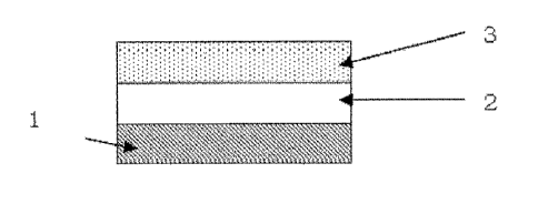
FIG. 1 is a schematic view showing a cross-section of
a laminated body obtained by forming a buffer layer comprised
of a laminated structure of group III nitride films on a sapphire
substrate by MOCVD, and further forming a p-type group III
nitride semiconductor of the present invention thereon by
MOCVD.
FIG. 2 is a graph showing a relationship of a hole
concentration of the p-type group III nitride semiconductor
with inverse of temperature for each of the examples and
comparative examples.
FIG. 3 is a graph showing a relationship of a resistivity
of the p-type group III nitride semiconductor with inverse
of temperature for each of the examples and comparative
- 12-
CA 02681711 2009-09-22
PCT/JP2008/055277
WP08006PT
examples.
FIG. 4 is a graph showing a relationship of Mg concentration
with "change ratio of a-axis crystal lattice constant" and
"change ratio of c-axis crystal lattice constant".
FIG. 5 is a graph showing a relationship of
[ (Al-A2) /Al] x100 of the p-type group III nitride semiconductor
(horizontal axis) with a resistivity (vertical axis) for each
of the examples and comparative examples.
FIG. 6 is a graph showing a relationship of
[ (C1-C2) /C1] x100 of the p-type group III nitride semiconductor
(horizontal axis) with a resistivity (vertical axis) for each
of the examples and comparative examples.
BEST MODE FOR WORKING THE INVENTION
[0019]
Hereinafter, the present invention will be described based
on an embodiment shown in the drawings.
A p-type group III nitride semiconductor of the present
invention is obtained by doping an acceptor impurity atom in
- 13 -
CA 02681711 2009-09-22
PCT/JP2008/055277
WP08006PT
a concentration of 5x10³-8 to 1x102 cm-3 to a group III nitride
semiconductor having a composition expressed by AlxGayInzN
(where each of X, Y and Z indicates a rational number satisfying
1.0>X0.5, 0.5.YØ0 and 0.5Z0.0, and satisfies a
relationship of X+Y+Z=1.0) , wherein a proportion of hole
concentration to an acceptor impurity atom concentration at
30 C is 0.001 or more. For a p-type group III nitride
semiconductor wherein an acceptor impurity atom is doped to
a group III nitride semiconductor having a high concentration
of Al content represented as X of 0.5 or more in the above
composition formula, there is not yet known the one wherein
hole concentration at 30 C is high and 0.001 or more times
larger than an acceptor impurity atom concentration.
[0020]
The group III nitride semiconductor as a base of the p-type
group III nitride semiconductor of the present invention may
be any expressed by the above composition, and it is preferable
to be crystalline material, particularly single crystal. Also,
as for its composition, because of ease of production, X, Y
=
- 14 -
CA 02681711 2009-09-22
PCT/JP2008/055277
WP08006PT
and Z in the above composition formula preferably satisfy a
relationship of 0 . 9>X0.5, O. 5Y0.1 and 0.1Z-0, particularly
preferablya relationship of O. 8>X0 . 6, 0.4--Y-0.2 and O. 05ZO.
[0021]
Note that contents of Al, In, Ga and N can be measured
by secondary ion mass spectrometry, etc.
[0022]
The p-type group III nitride semiconductor of the present
invention includes an acceptor impurity atom in a concentration
of 5x101-8 to 1x102 cm-3. When the acceptor impurity atom
concentration is out of the above range, no crystal lattice
deformation occurs to cause hopping conduction, and it is
impossible to obtain good p-type semiconductor properties even
in an ideal crystal state by optimizing crystal growth
conditions. In the p-type group III nitride semiconductor of
the present invention, for example, low resistivity value of
5x10³ Ocm or less can be attained at around 30 C. However,
it is conventionally considered to theoretically need to dope
an acceptor impurity atom in a high concentration of 1x10²¹
- 15 -
CA 02681711 2009-09-22
PCT/JP2008/055277
WP08006PT
cm.-3 or more to form holes for obtaining such a resistivity
value. Namelyõ with an acceptor impurity atom in a lower
concentration by single-digit or more, the present invention
attains higher conductive properties than conventionally
obtained.
[0023]
As the acceptor impurity atom included in the p-type group
III nitride semiconductor of the present invention, Mg, Zn,
Ca, Cd, Be, etc. can be used. Among these, Mg is preferable
to use since ionization energy of the acceptor impurity atom
is small and concentration control is relatively easy. The
acceptor impurity atom concentration may be in a range of 5 x 10¹⁸
to 1x102 cm-3, and is preferably 1.6x10¹⁹ to 7x1019 cm-3,
particularly preferably 2x10¹⁹ to 5x1019 cm-3, for stably
obtaining high hole concentration. When the acceptor impurity
atom concentration is within the range of 5x10¹⁸ to 1.5x10¹⁹
cm73, crystal lattice deformation due to introduction of the
acceptor impurity atom is relatively small, and also,
influences due to small changes in crystal growth conditions
- 16-
CA 02681711 2009-09-22
PCT/JP2008/055277
= WP08006PT
are relatively large. Therefore, even when producing a p-type
group III nitride semiconductor in the same procedures,
deformation volume may vary and desired deformation may not
be obtained.
[0024]
The hole concentration of the p-type group III nitride
semiconductor of the present invention at 30 C is more than
0.001 times, preferably more than 0.0015 times and most
preferably more than 0.002 times larger than the acceptor
impurity atom concentration. The hole concentration at 30 C
can be measured by a known Hall effect measurement wherein
hole concentration is calculated from a resistivity value and
a Hall induced voltage.
[0025]
As described above, the hole concentration is considered
to be determined by influences of acceptor impurity atom
concentration and various structural factors, but the mechanism
is unknown. Therefore, "a proportion of hole concentration
at 30 C to an acceptor impurity atom concentration" is used
- 17-
CA 02681711 2009-09-22
PCT/JP2008/055277
WP08006PT
to indirectly determine such a structural characteristic in
the present invention.
[0026]
In the p-type group III nitride semiconductor of the
present invention, dislocation density is preferably 1010cm72
or less, particularly preferably 109 cm.-2 or less, and oxygen
concentration is preferably 1018 cm-3 or less, particularly
preferably 1017 cm-3 or less, in view of inhibiting formation
of "donor-type compensation center". Note that the
dislocation density can be measured by plane cross section
observation via a transmission electron microscope. Also,
oxygen concentration can be measured by secondary ion mass
spectrometry.
[0027]
As a result of X-ray diffraction analysis for crystal
structure of the p-type group III nitride semiconductor of
the present invention actually produced by MOCVD, it was
confirmed that the a-axis lattice constant and c-axis lattice
constant change from an a-axis lattice constant and a c-axis
- 18-
CA 02681711 2009-09-22
pcT/JP2008/055277
wp08006PT
lattice constant of a group III nitride semiconductor having
same composition but including no acceptor impurity atom (a
group III nitride semiconductor manufactured in the same
procedures except for not doping an acceptor impurity atom) .
Namely, it was confirmed that "Al" is larger than "A2" by 0.10%
or more or that "Cl" is smaller than "C2" by 0.05% or more
when an a-axis lattice constant and a c-axis lattice constant
of the p-type group III nitride semiconductor of the present
invention are defined as "Al" and "Cl" respectively, and when
an a-axis lattice constant and a c-axis lattice constant of
a group III nitride semiconductor having same composition but
including no acceptor impurity atom are defined as "A2" and
"C2" respectively. From this observation, it would appear that
hopping conduction occurs at around 30 C in the p-type group
III nitride semiconductor of the present invention, as observed
in amorphous semiconductor.
[0028]
Namely, it was believed in the past that hole conduction
was caused by thermal excitation from a certain acceptor level
- 19 -
CA 02681711 2009-09-22
PCT/JP2008/055277
WP08006PT
determined by the composition of group III nitride in the p-type
group III nitride semiconductor. On the other hand, in the
p-type group III nitride semiconductor of the present invention,
(1) conduction caused by the above conventional thermal
excitation is dominant in a range of 200 C or more, and (2)
activation energy of the acceptor impurity atom is remarkably
lower than the activation energy expected based on the above
conventional mechanism in a range of around 30 C to 200 C,
which is much as low as 200 meV or less, for example. As a
result, concentration of the acceptor impurity atom, which
effectively functions as an acceptor, may be increased.
[0029]
In the conduction mechanism in the above (2) temperature
range, energy band ( impurity band) is formed due to the acceptor
impurity atom in the p-type group III nitride semiconductor,
and the conduction mechanism to cause hole conduction via
localized state in the impurity band is considered dominant
(Nobuo Mi koshiba , "Handotai no Butsuri ( Semiconductor Physics)
[revised edition] ") . Then, the present invention succeeds in
- 20 -
CA 02681711 2009-09-22
PCT/JP2008/055277
WP08006PT
purposely activating such a mechanism by maintaining the
acceptor impurity atom concentration within the specific range
and optimizing various crystal growth conditions in MOCVD.
As a result, activation energy at around 30 C is considerably
reduced, and holes are formed in a concentration as high as,
for example, 5x1015cm-3or more to Mg concentration (acceptor
impurity atom concentration) at activation rate as high as
0.001 or more, resulting in resistivity value as low as 5x10³
Qcm or less, for example.
[0030]
Note that "change ratio of a-axis crystal lattice
constant" defined by a relationship of [(A1-A2)/A1]x100 is
preferably 0 . 10% to 1 . 0%, particularly preferably 0 . 2 to 0 . 5%,
and also "change ratio of c-axis crystal lattice constant"
defined by a relationship of [(C1-C2) /01]x100 is preferably
-0.05% to -0.5%, particularly preferably -0.10 to -0.3%, in
the p-type group III nitride semiconductor of the present
invention since the above (2) mechanism is easily attained.
[0031]
-21 -
CA 02681711 2009-09-22
PCT/JP2008/055277
WP08006PT
The p-type group III nitride semiconductor of the present
invention can be preferably manufactured by MOCVD. However,
even when using MOCVD and controlling the acceptor impurity
atom concentration within the predetermined range, it may be
impossible to obtain the p-type group III nitride semiconductor
of the present invention depending onmanufacturing conditions .
Therefore, it is necessary to select manufacturing conditions
with attention not to incorporate an impurity atom other than
the acceptor impurity atom or not to form dislocation in the
crystal during manufacturing.
[0032]
When manufacturing the p-type group III nitride
semiconductor of the present invention by MOCVD, the p-type
group III nitride semiconductor of the present invention having
the predetermined composition is grown on a surface of a
substrate for crystal growth. As the substrate for crystal
growth, for example, thermally-stable material resistant to
temperature history during a film formation step, such as
sapphire, SiC, Si, GaN, AlN, AlGaN, ZnO and ZrB2, and
- 22 -
CA 02681711 2009-09-22
PCT/JP2008/055277
WP08006PT
specifically, it is preferable to use thermally-stable material
having a melting point or decomposition temperature of at least
1000 C or more.
[0033]
Also, it is preferable to preliminarily form a buffer
1
layer on the above substrate. Material and layer structure
of the buffer layer are not particularly limited as long as
these are the constitution to inhibit generation of N defect
as compensation center of the acceptor impurity atom of the
p-type group III nitride semiconductor of the present invention
grown on the buffer layer. Also, when using the p-type group
III nitride semiconductor of the present invention as a p-type
layer constituting a device such as light emitting device,
it may be formed on a N-type layer or an emission layer such
as quantum well structure.
[0034]
As group III raw materials, group V raw materials and
acceptor impurity raw materials used for MOCVD, any raw
materials can be used without particular limitation, which
- 23 -
CA 02681711 2009-09-22
,
PCT/JP2008/055277
.
WP08006PT
are known to be used for forming a p-type group III nitride
semiconductor depending on the composition of p-type AlxGayInzN .
As the group III raw materials, it is preferable to use
trimethylaluminum or triethylaluminum, and trimethylgallium,
triethylgallium or trimethylindium. Also, as the group V raw
materials and the acceptor impurity raw materials, it is
preferable to use ammonia and bis ( cyclopentadienyl ) magnesium,
respectively.
[0035]
Hereinafter, one example will be explained in detail in
reference to FIG. 1, in which a buffer layer comprising laminated
structure of a group III nitride film is formed on a sapphire
substrate by MOCVD, and the p-type group III nitride
semiconductor of the present invention is formed further
thereon by MOCVD.
[0036]
In the above example, after placing the sapphire substrate
1 in a MOCVD system, the substrate is first heated to 1050 C
ormore, further preferably 1150 C or more , and held in a hydrogen
- 24 -
CA 02681711 2009-09-22
PCT/JP2008/055277
WP08006PT
atmosphere to perform cleaning the substrate surface. Then,
trimethylaluminum, trimethylgallium, ammonia, andcarriergas
of raw material gas such as hydrogen and nitrogen are introduced
in the MOCVD system at 1050 C or more, further preferably 1150 C
or more, so that the group III nitride buffer layer 2 is formed.
[0037]
The group III nitride buffer layer 2 may have crystal
characteristic at least not spoiling properties of the p-type
group III nitride semiconductor layer 3 of the present invention
laminated on the buffer layer. It is preferable that half
bandwidths of (002) and (102) planes are 500 arcsec or less
and 2000 arcsec or less, respectively, in X-ray rocking curve
measurement, and further that emission intensity caused by
group III or group V defect and impurity etc. is minimized
in photoluminescence (PL) measurement etc.
[0038]
Next, in addition to the above group III and group V raw
materials and carrier gas, bis ( cyclopentadienyl ) magnesium is
introduced in the MOCVD system to form an AlxGayInzN layer 3
- 25 -
CA 02681711 2009-09-22
PCT/JP2008/055277
WP08006PT
to which Mg is doped as the acceptor impurity atom. The flow
of bis (cyclopentadienyl)magnesium here is controlled so as
to make Mg concentration in the AlxGayInzN layer within a range
of 5.0x10¹⁸ to l. 0x102 cm-3, further preferably within a range
of 2.0x10¹⁹ to 5.0x1019 cm-3.
[0039]
It is desirable to control growth temperature, V/III ratio
and growth rate when forming a Mg-doping layer here so as to
minimize emission caused by impurity in PL measurement after
growth. Specifically, it is preferable to set the growth
temperature in a range of 1050 to 1150 C, the V/III ratio in
a range of 1000 to 4000, and the growth rate in a range of
0.5 to 1.5 pm/hr. When deviating from the above conditions,
high p-type semiconductor properties may not be obtained even
when controlling the acceptor impurity atom concentration
within the predetermined range.
[0040]
The p-type group III nitride semiconductor of the present
invention obtained by such a method has good p-type
- 26 -
CA 02681711 2009-09-22
PCT/JP2008/055277
.
WP08006PT
semiconductor properties, so that it can be preferably used
as a p-type clad layer of a light emitting device based on
the group III nitride semiconductor. It is also possible to
manufacture a light emitting diode and laser diode that emits
light in the deep ultraviolet region of 300nm or less by using
the p-type group III nitride semiconductor of the present
invention.
EXAMPLE
[0041]
Hereinafter, the present invention will be explained in
detail according to examples and comparative examples, but
the present invention is not limited to these examples.
[0042]
Example 1
A sapphire C-plane single crystal substrate was used for
a crystal substrate for growth . After placing it on a susceptor
in a MOCVD system, the sapphire substrate was heated to 1150 C
and held for 10 minutes while running hydrogen at a flow of
- 27 -
CA 02681711 2009-09-22
PCT/JP2008/055277
WP08006PT
13 slm, for surface cleaning. Next, an AIN film was formed
to have a thickness of 0.45 pm under conditions of temperature
of the sapphire substrate at 1150 C, trimethylaluminum flow
rate at 15 pmol/min, ammonia flow of 1 slm, entire flow of
slm and pressure at 50 Torr.
[0043]
Then, an A10.7Ga0.3N buffer layer was formed to have a
thickness of 0.4 pm under conditions of the temperature of
the sapphire substrate at 1120 C, trimethylgallium flow rate
at 10 pmol/min, trimethylaluminum flow rate at 15 pmol/min,
ammonia flow of 1.5 slm, entire flow of 10 slm and pressure
at 50 Torr.
[0044]
Next, a Mg-doping A10.7Ga0.3N layer was formed to have a
thickness of 0.5 pm under the same conditions as in forming
the buffer layer except for simultaneously supplying
bis ( cyclopentadienyl ) magnesium in condition of 0.8 pmol/min.
[0045]
The substrate was taken out from the MOCVD system, followed
- 28 -
CA 02681711 2009-09-22
PCT/J52008/055277
WP080D6PT
by X-ray reciprocal lattice mapping measurement in (204) plane
by using high-resolution X-ray diffraction analysis system
(X 'Pert made by Spectris Co. , Ltd., PANalytical division) under
conditions of accelerating voltage at 45 kV and accelerating
current at 40 mA. Then, the substrate was cut into several
square-shaped samples with about 7 mm square, followed by heat
treatment in a nitrogen atmosphere for 20 minutes at 800 C.
[0046]
Randomly-selected one of the heat-treated substrate
samples was subject to quantitative analysis of Mg by secondary
ion mass spectrometry using cesium ion as primary ion. Mg
concentration was determined based on nitrogen secondary ion
intensity of the GaN standard sample. Next, a Ni (20 nm)/Au
(100 nm) electrode was formed by a vacuum deposition method,
followed by heat treatment in a nitrogen atmosphere for 5 minutes
at 500 C. After forming the electrode, Hall measurement was
performed by using Hall effect measurement system (Resitest
8300 made by Toyo Corporation) under conditions of current
value at lx10-7to lx10-, frequency at 50 to 100 mHz, magnetic
- 29 -
CA 02681711 2009-09-22
PCT/JP2008/055277
WP08006PT
field at 0.38T and measurement temperature at 30 to 525 C.
[0047]
The activation energy of Mg and activation rate of Mg
(proportion of hole concentration to Mg concentration) obtained
by Hall measurement, and plots of hole concentration and
resistivity value to measurement temperature are shown in Table
1, and FIGs 2 and 3, respectively.
[0048]
Also, "change ratio of a-axis crystal lattice constant"
and "change ratio of c-axis crystal lattice constant"
calculated from a difference in lattice constants of the undoped
buffer layer and the Mg-doping layer obtained by X-ray
reciprocal lattice mapping measurements are shown in Table
2 as well as Mg concentration obtained by secondary ion mass
spectrometry ( SIMS measurement) . Plots of hole concentration
and resistivity value to the above difference in lattice
constants are shown in FIG. 5 and FIG. 6.
[0049]
[Table 1]
- 30 -
CA 02681711 2009-09-22
PCT/JP2008/055277
.
WP08006PT
Ea(T1) Ea(T2) Holeconcentration**/Mg
concentration
Example 1 51 403 3.63x10⁻³
Example 2 39 360 6.07x10⁻³
Example 3 30 491 4.34x10⁻³
Example 4 151 543 1.04x10⁻³
Comperative 367 530 1.58x10⁻⁵
Example 1
Comperative 401 596 4.84x10⁻⁷
Example 2
Comperative 438 512 9.24x10⁻⁵
Example 3
** hole concentration at 30 C
[0050]
[Table 2]
Evaluation Items
{(A1-A2)/A2fx100 {(C1-C2)/C2}x100 Mg
concentration
[1019cm-3]
- 31 -
CA 02681711 2009-09-22
PCT/JP2008/055277
WP08006PT
Example 1 0.294 -0.126 3.6
Example 2 0.406 -0.224 3.0
Example 3 0.235 -0.115 2.6
Example 4 0.122 -0.056 0.8
Comperative 0.098 -0.047 1.5
Example 1
Comperative 0.135 -0.063 3.2
Example 2
Comperative 0.204 -0.104 3.6
Example 3
"Al": a-axis lattice constant of Mg-doping A10.7Ga0.3N layer
"A2": a-axis lattice constant of A10.7Ga0.3N layer
"Cl": c-axis lattice constant of Mg-doping A10.7Ga0.3N layer
"C2": c-axis lattice constant of A10.7Ga0.3N layer
[0051]
Example 2
Except for changing bis ( cyclopentadienyl ) magnesium flow
to 0.6 pmol/min, p-type AlGaN was produced under the same
conditions as in Example 1. The obtained results are shown
- 32 -
CA 02681711 2009-09-22
PCT/JP2008/055277
WP08006PT
in Tables 1 to 2 and FIGs. 3 to 6.
[0052]
Example 3
Except for changing bis ( cyclopentadienyl ) magnesium flow
to 0.4 pmol/min, p-type AlGaN was produced under the same
conditions as in Example 1. The obtained results are shown
in Tables 1 to 2 and FIGs. 3 to 6.
[0053]
Comparative Example 1
Except for changing bis ( cyclopentadienyl ) magnesium flow
to 0.2 pmol/min, p-type AlGaN was produced under the same
conditions as in Example 1. The obtained results are shown
in Tables 1 to 2 and FIGs. 3 to 6.
[0054]
Example 4
Except for changing bis ( cyclopentadienyl ) magnesium flow
to 0.1 umol/min, p-type AlGaN was produced under the same
conditions as in Example 1. The obtained results are shown
in Tables 1 to 2 and FIGs. 3 to 6.
- 33 -
CA 02681711 2009-09-22
,
PCT/JP2008/055277
WP08006PT
[0055]
Comparative Example 2
Except for changing growth temperature of Mg-doping
A10.7Ga0.3N layer to 1200 C, p-type AlGaN was produced under
the same conditions as in Example 1. The obtained results are
shown in Tables 1 to 2.
[0056]
Comparative Example 3
Except for changing growth temperature of Mg-doping
A10.7Ga0.3N layer to 1000 C, p-type AlGaN was produced under
the same conditions as in Example 1. The obtained results are
shown in Tables 1 to 2.
[0057]
From Table 1, activation energy in the after-mentioned
Ti region was as low as 200 meV or less, and activation rate
was as high as 0.001 or more in Examples 1, 2, 3 and 4.
[0058]
FIG. 2 and 3 show temperature dependency of the hole
concentration and resistivity value in each of the examples
- 34 -
CA 02681711 2009-09-22
PCT/JP2008/055277
WP08006PT
and comparative example. As clearly shown in FIG. 2, while
the hole concentration of Comparative Example 1 shows
rectilinear change, the slope in the range where 1000/T is
2.0 to 3.3 (corresponding to 30 to 230 C, Ti region) is largely
different from the slope in the range where 1000/T is 1.25
to 2.0 (corresponding to 230 to 525 C, T2 region) in Examples
1, 2, 3 and 4. It may indicate that conduction mechanism
different from that of Comparative Example 1 is dominant in
the range of 30 to 230 C.
[0059]
Note that activation energy of Mg and activation rate
of Mg (proportion of hole concentration to Mg concentration)
in Ti and T2 regions shown in Table 1 were calculated by the
following calculation formula.
[0060]
Calculation Formula: p = A x exp [Ea/(kbT)]
where p : hole concentration [cm-3], A: arbitrary constant,
Ea: activation energy [meV], kb: Boltzmann coefficient and T:
temperature [K].
- 35 -
CA 02681711 2009-09-22
PCT/JP2008/055277
= WP08006PT
[0061]
Also, from FIG. 3, resistivity values at around 30 C were
5x10³ Qom or less in Example 4, and further 150 Qom or less
in Examples 1, 2 and 3. These were lower by 1 to 2 digits than
those in conventional art.
[0062]
<Comparison between Example 1 and Comparative Examples
2 to 3>
As shown in Table 1, activation energy in Comparative
Examples 2 and 3 was 400 meV or more and higher than that in
Example 1. As a result, activation rate of Mg was lower by
2 or more digits than that in Example 1. Such remarkable
differences in p-type semiconductor properties were caused
by introduction of oxygen impurity and N defect, etc. in the
Mg-doping layer due to producing in the crystal growth
temperature out of the proper range, resulting in formation
of many "donor-type compensation centers".
[0063]
<Comparison between Examples 1 to 4 and Comparative
- 36 -
CA 02681711 2009-09-22
PCT/JP2008/055277
WP08006PT
Example 1>
The results of Table 2 are summarized in FIG. 4. As shown
in FIG. 4, by doping Mg, the Mg-doping layer always had a tendency
to lengthen to the a-axis direction or shorten to the c-axis
direction compared to undoping samples. In addition, the
amounts of change, i.e. "change ratio of a-axis crystal lattice
constant" and "change ratio of c-axis crystal lattice constant",
showed small variation but had a tendency to increase with
increase in Mg concentration. Mg-doping amount was 1.5x10'9
-3 i
cm n Comparative Example 1, however, crystal lattice
deformation was relatively small when doping the above amount,
and effects due to slight change in crystal growth conditions
were relatively strong as described above. Therefore,
although crystal growth conditions were the same as Example
4 except for making the doping amount larger, deformation volume
of the crystal lattice deformation was inverted due to
uncontrollable small differences in growth conditions, so that
hole concentration/Mg concentration ratio was out of the range
of the present invention.
- 37 -
CA 02681711 2009-09-22
PCT/JP2008/055277
WP08006PT
[0064]
Note that it was found from Table 2 that Mg concentrations
in crystal were nearly identical in Example 1 and Comparative
Examples 2 and 3 where flow condition of
bis (cyclopentadienyl)magnesium was same, and that lattice
constant of the Mg-doping layer was not largely different.
[0065]
FIG. 5 and 6 respectively show plots of hole concentration
and resistivity value, obtained by Hall measurements at 30 C,
to the above "change ratio of a-axis crystal lattice constant"
and "change ratio of c-axis crystal lattice constant". As
clearly shown in these figures, the "change ratios of a-axis
crystal lattice constant" were 0.1% or more, and the "change
ratios of c-axis crystal lattice constant" were -0.05% or less
in Examples 1, 2, 3 and 4. Such change ratios resulted in rapid
reduction of resistivity values and simultaneously, rapid
increase in hole concentrations. The resistivity value and
hole concentration were nearly constant, in which the "change
ratio of a-axis crystal lattice constant" and the "change ratio
- 38 -
CA 02681711 2009-09-22
PCT/JP2008/055277
.
WP08006PT
of c-axis crystal lattice constant" were respectively 0.2%
or more and -0.1% or less. On the other hand, in Comparative
Example 1, the "change ratio of a-axis crystal lattice constant"
was less than 0.01%, the "change ratio of c-axis crystal lattice
constant" exceeded -0.05%, the resistivity value was extremely
high and about 6.5x10⁴ Qom, and the hole concentration was as
low as about 2.4x101-4 cm-3.
- 39 -