Note: Descriptions are shown in the official language in which they were submitted.
CA 02682092 2009-10-30
AND-TYPE ONE TIME PROGRAMMABLE MEMORY CELL
FIELD OF THE INVENTION
[001] The present invention relates generally to non-volatile memory. More
specifically, the
invention is directed to one-time programmable (OTP) memories.
BACKGROUND OF THE INVENTION
[002] Anti-fuse memory is one type of one-time programmable (OTP) memory in
which the
device can be permanently programmed (electrically) with data once. This data
is
programmed by an end user for a particular application. There are several
types of OTP
memory cells which can be used. OTP memories provide users with a level of
flexibility since
any data can be programmed.
[003] Anti-fuse memory can be utilized in all one time programmable
applications, including
RF-ID tags. RF-ID tagging applications are gaining more acceptance in the
industry,
particularly in sales, security, transport, logistics, and military
applications for example. The
simplicity and full CMOS compatibility anti-fuse memory allows for application
of the RF-ID
tag concept to integrated circuit manufacturing and testing processes.
Therefore, IC
manufacturing productivity can be increased by utilizing anti-fuse memory in
combination
with an RF communication interface on every wafer and/or every die on the
wafer allowing
for contact-less programming and reading chip specific or wafer specific
information during
IC manufacturing and packaging, as well as during printed circuit board
assembly.
[004] Figure 1 is a circuit diagram of a known anti-fuse memory cell, while
Figures 2 and 3
show the planar and cross-sectional views respectively of the anti-fuse memory
cell shown in
Figure 1. The anti-fuse memory cell of Figure 1 includes a pass, or access
transistor 10 for
coupling a bitline BL to a bottom plate of anti-fuse device 12. Anti-fuse
device 12 is
considered a gate dielectric breakdown based anti-fuse device. A wordline WL
is coupled to
the gate of access transistor 10 to turn it on, and a cell plate voltage Vcp
is coupled to the top
plate of anti-fuse device 12 for programming anti-fuse device 12.
[005] It can be seen from Figures 2 and 3 that the layout of access transistor
10 and anti-
fuse device 12 is very straight-forward and simple. The gate 14 of access
transistor 10 and
the top plate 16 of anti-fuse device 12 are constructed with the same layer of
polysilicon,
which extend across active area 18. In the active area 18 underneath each
polysilicon layer,
-1-
CA 02682092 2010-06-18
is formed a thin gate oxide 20, also known as a gate dielectric, for
electrically isolating the
polysilicon from the active area underneath. On either side of gate 14 are
diffusion regions
22 and 24, where diffusion region 24 is coupled to a bitline. Although not
shown, those of skill
in the art will understand that standard CMOS processing, such as sidewall
spacer formation,
lightly doped diffusions (LDD) and diffusion and gate silicidation, can be
applied. While the
classical single transistor and capacitor cell configuration is widely used, a
transistor-only
anti-fuse cell is further desirable due to the semiconductor array area
savings that can be
obtained for high-density applications. Such transistor-only anti-fuses should
be reliable while
simple to manufacture with a low cost CMOS process.
[006] Figure 4B shows a cross-sectional view of an anti-fuse transistor taken
along line B-B
of the anti-fuse transistor show in Figure 4A that can be manufactured with
any standard
CMOS process. This anti-fuse transistor and its variants are disclosed in
commonly owned
U.S. Patent No. 7,402,855 issued on July 22, 2008, and commonly owned U.S.
Patent
Publication No. 20070257331 Al published on November 8, 2007. In the presently
shown
example, the anti-fuse transistor is almost identical to a simple thick gate
oxide, or
input/output MOS transistor with one floating diffusion terminal. The
disclosed anti-fuse
transistor, also termed a split-channel capacitor or a half-transistor, can be
reliably
programmed such that the fuse link between the polysilicon gate and the
substrate can be
predictably localized to a particular region of the device. The cross-section
view of Figure 4B
is taken along the channel length of the device. The channel is generally
understood to be
the area underneath an overlying polysilicon gate, having a length defined by
edges of the
polysilicon gate adjacent respective diffusion regions. Expressed in the
alternative, the
channel is underlying the polysilicon gate.
[007] Anti-fuse cell 30 includes a variable thickness gate oxide 32 formed on
the substrate
channel region 34, a polysilicon gate 36, sidewall spacers 38, a field oxide
region 40 a
diffusion region 42, and an LDD region 44 in the diffusion region 42. A
bitline contact 46 is
shown to be in electrical contact with diffusion region 42. The variable
thickness gate oxide
consists of a thick gate oxide 32 and a thin gate oxide 33 such that a portion
of the channel
length is covered by the thick gate oxide and the remaining portion of the
channel length is
covered by the thin gate oxide. Generally, the thin gate oxide is a region
where oxide
breakdown can occur. The thick gate oxide edge meeting diffusion region 42 on
the other
hand, defines an access edge where gate oxide breakdown is prevented and
current
between the gate 36 and diffusion region 42 is to flow for a programmed anti-
fuse transistor.
- 2-
CA 02682092 2010-06-18
While the distance that the thick oxide portion extends into the channel
region depends on
the mask grade, the thick oxide portion is preferably formed to be at least as
long as the
minimum length of a high voltage transistor formed on the same chip.
(008] In this example, the diffusion region 42 is connected to a bitline
through a bitline
contact 46, or other line for sensing a current from the polysilicon gate 36,
and can be doped
to accommodate programming voltages or currents. This diffusion region 42 is
formed
proximate to the thick oxide portion of the variable thickness gate oxide. To
further protect
the edge of anti-fuse cell 30 from high voltage damage, or current leakage, a
resistor
protection oxide (RPO), also known as a salicide protect oxide, can be
introduced during the
fabrication process to further space metal particles from the edge of sidewall
spacer 38. This
RPO is preferably used during the salicidiation process for preventing only a
portion of
diffusion region 42 and a portion of polysilicon gate 36 from being salicided.
It is well known
that salicided transistors are known to have higher leakage and therefore
lower breakdown
voltage. Thus having a non-salicided diffusion region 42 will reduce leakage.
Diffusion region
42 can be doped for low voltage transistors or high voltage transistors or a
combination of
the two resulting in same or different diffusion profiles.
[009] A simplified plan view of the anti-fuse cell 30 is shown in Figure 4A.
Bitline contact 46
can be used as a visual reference point to orient the plan view with the
corresponding cross-
sectional view of Figure 4B. The active area 48 is the region of the device
where the channel
region 34 and diffusion region 42 is formed, which is defined by an OD mask
during the
fabrication process. The dashed outline 50 defines the areas in which the
thick gate oxide is
to be formed via an OD2 mask during the fabrication process. More
specifically, the area
enclosed by the dashed outline 50 designates the regions where thick oxide is
to be formed.
OD simply refers to an oxide definition mask that is used during the CMOS
process for
defining the regions on the substrate where the oxide is to be formed, and OD2
refers to a
second oxide definition mask different than the first. According to an
embodiment of the
present invention, the thin gate oxide area bounded by edges of the active
area 48 and the
rightmost edge of the OD2 mask, is minimized. In the presently shown
embodiment, this area
can be minimized by shifting the rightmost OD2 mask edge towards the parallel
edge of
active area 48. Figure 4C is a schematic showing a transistor symbol
representing the anti-
fuse cell 30 shown in Figures 4B and 4A. As can be seen in Figure 4C, anti-
fuse cell 30 has
its gate connected to a wordline and its diffusion region 42 connected to a
bitline. Commonly
owned U.S. Patent Application No. 20070257331 Al published on November 8,
2007,
- 3-
CA 02682092 2010-06-18
describes alternate single transistor anti-fuse memory cells which can be used
in a non-
volatile memory array.
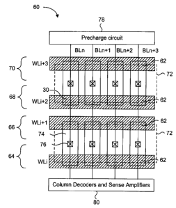
[0010] Figure 5 is a plan view layout of a single transistor anti-fuse memory
cell memory
array according to an embodiment of the present invention. In the present
example, only four
wordlines and four bitlines are shown. Each single transistor anti-fuse cell
30 in memory
array 60 has one polysilicon gate 62, and have the same structure as anti-fuse
cell 30 of
Figures 4B and 4A. In memory array 60, the polysilicon line forming
polysilicon gates 62 of
each anti-fuse memory cell are common to all the anti-fuse memory cells of the
row. Memory
array 60 is shown to include sixteen anti-fuse memory cells, where four are
arranged in each
of first row 64, second row 66, third row 68 and fourth row 70. Wordlines WLi,
WLi+1, WLi+2
and WLi+3 are connected to the polysilicon gates 62 of rows 64, 66, 68 and 70
respectively.
The dashed outlines 72 define the areas in the memory array in which a thick
gate oxide is to
be formed via a thick gate oxide definition mask during the fabrication
process. In the
configuration shown in Figure 5, each pair of memory cells from rows 64 and 66
share a
common diffusion region 74 and a common bitline contact 76. Each bitline
contact is
connected to a different bitline, such as bitlines BLn, BLn+1, BLn+2 and
BLn+3. Connected
to each of the bitlines is a precharge circuit 78, and a column decoder and
sense amplifier
circuit block 80. The precharge circuit 78 is responsible for precharging all
the bitlines to a
predetermined voltage for a read operation, while the column decoder and sense
amplifier
circuit block 80 includes multiplexing devices for sharing one sense amplifier
with one or
more bitlines. The actual layout of a memory array using the architecture of
Figure 5 can
have the precharge circuit 78 located at one end of the bitlines opposite to
the column
decoder and sense amplifier circuit block 80, or adjacent or integrated with
the column
decoder and sense amplifier circuit block 80.
[0011] An overview of the program and read operations is now discussed with
reference to
the anti-fuse cell 30 of Figure 4B and 4A, and memory array 60 of Figure 5.
Generally, the
anti-fuse transistors are programmed by rupturing the gate oxide, preferably
at one of the
thin/thick gate oxide boundary and the thin gate oxide/source diffusion edge.
This is
accomplished by applying a high enough voltage differential between the gate
and the
channel of the cells to be programmed and a substantially lower voltage
differential, if any,
on all other cells. Therefore, once a permanent conductive link is formed, a
current applied
to the polysilicon gate will flow through the link and the channel to the
diffusion region, which
can be sensed by conventional sense amplifier circuits. In the present
example,
- 4-
CA 02682092 2009-10-30
programming of anti-fuse cell 30 is achieved by grounding selected bitlines to
OV, and driving
a selected row to a programming voltage level (VPP) that is typically greater
than the VDD
voltage supply provided to other circuits. Under these conditions, the thin
gate oxide 33 is
intended to breakdown in the presence of the large electrical field formed
between the
channel region 34 and the wordline, thereby creating an electrically
conductive connection
between channel region 34 and polysilicon gate 36. This electrically
conductive connection
can be referred to as a conductive link or anti-fuse. In Figure 5 for example,
if BLn is
grounded and WLi is selected to be driven to VPP, then the anti-fuse cell 30
at the
intersection of BLn and WLi will be programmed once its conductive link is
formed. Hence
any anti-fuse transistor connected to WLi can be programmed if its
corresponding bitline is
grounded. On the other hand, inhibiting programming of any anti-fuse
transistor connected to
WLi is done by biasing the bitlines connected to them to VDD. The reduced
electric field is
insufficient for the conductive link to be formed.
[0012] To read a programmed or unprogrammed anti-fuse transistor with a formed
conductive link, all the bitlines are precharged to VSS followed by driving a
selected wordline
to VDD. Any programmed anti-fuse transistor having a conductive link will
drive its
corresponding bitline to VDD through its VDD driven wordline via the
conductive link. The
increased bitline voltage can then be sensed. Any unprogrammed anti-fuse
transistor having
an absence of a conductive link will have no effect on its corresponding
bitline, which means
that it remains at the VSS precharge level.
[0013] The anti-fuse memory cell memory array of Figure 5 has a relatively
high density
when compared to a memory array consisting of two-transistor per cell anti-
fuse cells, such
as the ones shown in Figures 1, 2 and 3. In otherwords, for the same area, the
anti-fuse
memory cell memory array of Figure 5 has a greater number of memory cells.
While each
anti-fuse cell 30 is shown to have a bitline contact, the arrangement Figure 5
maximizes area
efficiency because pairs of anti-fuse cells 30 share a common diffusion region
connected to a
bitline. Those skilled in the art understand that design rules governing the
spacing of bitline
contacts from other transistors structures, such as wordlines, must be adhered
to.
Accordingly, further density increases are obtained by scaling of the
transistor feature sizes
with successive manufacturing process generations. If such processes cannot be
used, then
the density of the anti-fuse memory cell memory array of Figure 5 cannot be
further
increased. In applications where the memory array occupies a significant area
of the
semiconductor chip relative to other logic, there may be economic factors that
require a
-5-
CA 02682092 2009-10-30
further reduction of the memory array size without resorting to leading edge,
and expensive,
manufacturing processes.
[0014] It is, therefore, desirable to provide an anti-fuse memory cell which
can be used to
form a high density memory array.
SUMMARY OF THE INVENTION
[0015] It is an object of the present invention to obviate or mitigate at
least one disadvantage
of previous anti-fuse memory cells.
[0016] In a first aspect, the present invention provides an anti-fuse memory
cell. The anti-
fuse memory cell includes an access transistor, an anti-fuse device and a
wordline. The
access transistor has a first channel region with a first channel length
dimension, and is
located adjacent to a diffusion region. The anti-fuse device has a second
channel region with
a second channel length dimension perpendicular to the first channel length
dimension, and
is connected to the first channel region. A wordline overlies the first
channel region and the
second channel region. In one embodiment, the diffusion region is connected to
one of a
bitline and another access transistor corresponding to an adjacent anti-fuse
memory cell. In
another embodiment, the access transistor includes a thick gate oxide between
the wordline
and the first channel region. In this embodiment, the anti-fuse device has a
variable
thickness gate oxide, and a thick portion of the variable thickness gate oxide
is adjacent to
the thick gate oxide of the access transistor. The thick portion of the
variable thickness gate
oxide has a thickness substantially identical to the thick gate oxide. In a
further embodiment,
the wordline extends in a first direction, and the first channel length of the
first channel region
extends perpendicular to the wordline. In this embodiment, the second channel
length of the
second channel region extends parallel to the wordline and has a width
extending
perpendicular to the wordline. The width of the second channel region is less
than the length
of the first channel region, and field oxide isolates the second channel
region from another
second channel region corresponding to the adjacent anti-fuse memory cell.
[0017] In a second aspect, there is provided a memory array. The memory array
includes a
plurality of memory chains and wordlines. The plurality of memory chains are
connected in
parallel to a bitline, where each of the memory chains includes at least two
one time
programmable memory cells connected in series with a bitline contact
corresponding to the
bitline. Wordlines are coupled to the at least two one time programmable
memory cells, the
wordlines being drivable during a memory operation. In one embodiment, each of
the at least
-6-
CA 02682092 2009-10-30
two one time programmable memory cells includes an access transistor having a
first
channel region adjacent to a diffusion region and an anti-fuse device having a
second
channel region connected to the first channel region. The first channel region
and the second
channel region are underlying one of the wordlines. In a present embodiment of
the second
aspect, the wordlines extend in a first direction, and the first channel
region has a length
extending perpendicular to the wordlines. The second channel region has a
length extending
parallel to the wordlines and a width extending perpendicular to the
wordlines.
[0018] In a third aspect, there is provided a method for executing a memory
operation on
series connected one time programmable memory cells. The method includes
biasing a
bitline contact connected to the series connected one time programmable (OTP)
memory
cells to a voltage level; coupling the voltage level to a selected OTP memory
cell of the
series connected OTP memory cells; and driving a wordline connected to a
selected OTP
memory cell to a predetermined voltage level. The step of coupling includes
turning on
intermediate OTP memory cells connected between the selected OTP memory cell
and the
bitline contact. The method further includes turning off any tail OTP memory
cells connected
between the selected OTP memory cell and a last OTP memory cell positioned
most distant
from the bitline contact. The step of turning on can include driving wordlines
connected to the
intermediate OTP memory cells to a pass voltage level effective for passing
the voltage level
to the selected OTP memory cell.
[0019] In a present embodiment, the memory operation includes a programming
operation,
wherein the series connected OTP memory cells are programmed sequentially from
the
selected OTP memory cell to a first OTP memory cell adjacent to the bitline
contact. The
selected OTP memory cell is a last OTP memory cell most distant from the
bitline. In this
embodiment, the predetermined voltage level is a programming voltage level,
and the
voltage level of the bitline contact can be an inhibit voltage to prevent
programming of the
selected OTP memory cell or an enable voltage to facilitate programming of the
selected
OTP memory cell. The pass voltage level is equal to or greater than both the
inhibit voltage
and the enable voltage, and less than the programming voltage level.
Alternately, the pass
voltage level is maintained while the enable voltage is applied to the
selected OTP memory
cell. Alternately, the pass voltage level is greater than a threshold voltage
of an access
transistor of the intermediate OTP memory cells and less than the programming
voltage
level.
-7-
CA 02682092 2009-10-30
[0020] According to yet another embodiment, the memory operation includes a
read
operation, wherein the predetermined voltage level is a read voltage level,
and the voltage
level of the bitline contact is precharged to a first voltage level
corresponding to a first logic
state. The pass voltage level is less than the read voltage level and less
than a threshold
voltage of a programmed memory cell.
[0021] Other aspects and features of the present invention will become
apparent to those
ordinarily skilled in the art upon review of the following description of
specific embodiments of
the invention in conjunction with the accompanying figures.
BRIEF DESCRIPTION OF THE DRAWINGS
[0022] Embodiments of the present invention will now be described, by way of
example only,
with reference to the attached Figures, wherein:
Fig. 1 is a circuit diagram of a DRAM-type anti-fuse cell;
Fig. 2 is a planar layout of the DRAM-type anti-fuse cell of Figure 1;
Fig. 3 is a cross-sectional view of the DRAM-type anti-fuse cell of Figure 2
along line A-A;
Fig. 4A is a planar layout of the variable thickness gate oxide anti-fuse
transistor;
Fig. 4B is a cross-sectional view of a variable thickness gate oxide anti-fuse
transistor of Figure 4A;
Fig. 4C is a transistor symbol representing the variable thick gate oxide anti-
fuse transistor of Figures 4A and 4B;
Fig. 5 is a plan view of a single-transistor anti-fuse memory array using the
variable thickness gate oxide memory cell of Fig. 4A;
Fig. 6A is a planar layout of an AND type anti-fuse memory cell, according to
a
present embodiment;
Fig. 6B is an equivalent circuit schematic representing the AND type anti-fuse
memory cell of Figure 6A;
Fig. 7 is a planar layout of a memory chain including serially connected AND
type anti-fuse memory cells, according to a present embodiment;
Fig. 8 is a planar layout of an alternate memory chain including serially
connected AND type anti-fuse memory cells, according to a present embodiment;
-8-
CA 02682092 2009-10-30
Fig. 9A is a planar layout of the memory chain of Figure 7 rotated clockwise
by
90 degrees;
Fig. 9B is a cross-sectional view of the memory chain of Figure 9A taken
along line C-C;
Fig. 9C is a cross-sectional view of the memory chain of Figure 9A taken
along line D-D;
Fig. 10A is a planar layout of the memory chain of Figure 7 showing cross
section line E-E;
Fig. 10B is a cross-sectional view of the memory chain of Figure 10A taken
along line E-E;
Fig. 11A is a planar layout showing a portion of a memory array of memory
chains, according to a present embodiment;
Fig. 11 B is an equivalent circuit schematic of the memory array of Figure
11A;
Fig. 12A is an alternate planar layout showing a portion of a memory array of
memory chains, according to a present embodiment;
Fig. 12B is an equivalent circuit schematic of the memory array of Figure 12A;
Fig. 13 is a flow chart of a method for programming cells of a memory chain,
according to a present embodiment; and,
Fig. 14 is a flow chart of a method for reading one cell of a memory chain,
according to a present embodiment.
DETAILED DESCRIPTION
[0023] Generally, the embodiments of the present invention provides an AND-
type anti-fuse
memory cell, and a memory array consisting of AND-type anti-fuse memory cells.
Chains of
AND type anti-fuse cells are connected in series with each other, and with a
bitline contact, in
order to minimize the area occupied by the memory array. Each AND type anti-
fuse cell
includes an access transistor serially connectable to the bitline or the
access transistors of
other AND type anti-fuse cells, and an anti-fuse device. The channel region of
the access
transistor is connected to the channel region of the anti-fuse device, and
both channel
regions are covered by the same polysilicon wordline. The wordline is driven
to a
programming voltage level for programming the anti-fuse device, or to a read
voltage level
for reading the anti-fuse device. The programming voltage level and the read
voltage level
-9-
CA 02682092 2009-10-30
are sufficiently high to turn on the access transistor for coupling the anti-
fuse device to the
bitline during programming and read operations.
[0024] Because of the unique layout of the AND type anti-fuse memory cell,
each chain of
serially connected AND type memory cells minimizes the area it occupies on the
semiconductor chip. Furthermore, because each chain requires only a single
bitline contact,
the total number of bitline contacts required for a memory array comprising of
such chains is
reduced relative to prior art anti-fuse memory arrays. Therefore, a high
density anti-fuse
memory array is realized with the embodiments of the present invention.
[0025] Figure 6A is a plan view layout showing one AND type anti-fuse memory
cell, while
Figure 6B shows an equivalent circuit schematic of the memory cell shown in
Figure 6A,
according to an embodiment of the present invention. AND type anti-fuse memory
cell 100
has a "T" shaped active area 102 surrounded by insulating field oxide, and
includes an
access transistor 104 and an anti-fuse device 106. Therefore AND type anti-
fuse memory
cell 100 is a two transistor cell. In this embodiment and all following
embodiments, the AND
type anti-fuse memory cell is assumed to be n-type, or n-channel. Those
skilled in the art will
understand that they can be formed as p-type, or p-channel devices. When
fabricated in a
memory array, a polysilicon wordline 108 is formed such that it overlies the
entire active area
102 to form the gates of access transistor 104 and anti-fuse device 106. The
wordline 108
can be formed of other conductive materials, and is therefore not limited to
polysilicon. For
example, metal gates can be used instead. While not shown in Figure 6A, gate
oxide is
formed between the active area 102 and the polysilicon gate 108. Polysilicon
gate 108 is
broken over the active area 102 in order to clearly show the features of AND
type anti-fuse
memory cell 100. The access transistor 104 channel region has a length
dimension 110 that
extends perpendicular to the direction of the polysilicon wordline 108, and a
width dimension
112 that extends parallel to the direction of the polysilicon wordline 108.
The anti-fuse device
106 channel region has a length dimension 114 that extends parallel to the
direction of the
polysilicon wordline 108, and a width dimension 116 that extends perpendicular
to the
direction of the polysilicon wordline 108. In one presently shown embodiment,
anti-fuse
device 106 can have a variable thickness gate oxide, such as anti-fuse cell 30
shown in
Figures 4A and 4B. In otherwords, the channel length dimensions of the access
transistor
104 and the anti-fuse device 106 are perpendicular to each other. Therefore
the transistor
symbol used for the anti-fuse device 106 in Figure 6B is the same as the
symbol used for
representing the variable thickness gate oxide anti-fuse cell 30 of Figure 4C.
-10-
CA 02682092 2009-10-30
[0026] It should be noted that the channel length and width dimensions of the
access
transistor 104 and the anti-fuse device 106 extend in different directions
relative to each
other. Accordingly, along the channel length dimension 114 of anti-fuse device
106, one end
of the channel (right-most end for example) is adjacent to field oxide and the
other end of the
channel (left-most end) is connected to the channel of access transistor 104.
Along the
channel length dimension 110 of access transistor 104, one end of the channel
(bottom end
for example) is adjacent to either field oxide or a diffusion region (not
shown), while the other
end of the channel (top end for example) is adjacent to either a diffusion
region (not shown)
or a diffusion region with a bitline contact (not shown). In the circuit
schematic of Figure 6B,
terminals 118 and 120 represent either diffusion regions or field oxide,
depending on the
position of anti-fuse cell 100 in a chain of series connected AND type anti-
fuse memory cells
100. The gate terminals of access transistor 104 and anti-fuse device 106 are
connected to a
wordline WL, shown as polysilicon wordline 108 in Figure 6A.
[0027] Figure 7 is a plan view layout showing a series connected chain of
three AND type
anti-fuse memory cells 200, 202 and 204 connected in series with each other to
a bitline
contact 206. In the presently shown example, cells 200, 202 and 204 form a
series chain of
AND type anti-fuse memory cells, simply referred to as a chain of cells from
this point
forward. Polysilicon wordlines 208, 210 and 212 are formed over respective
cells 200, 202
and 204. Formed between cells 200, 202 and cells 202, 204 are diffusion
regions 214 and
216 for electrically coupling the cells to each other. An optional diffusion
region 218 is formed
for the last cell 204 of the chain, which can be omitted without any adverse
effect on the
operation of the last cell 204. Accordingly, the cells are ordered from a
first cell in the chain,
that being cell 200 for example, to the last cell 204. For the presently
described
embodiments, the last cell refers to the cell in the chain that is positioned
furthest from the
bitline contact while the first cell refers to the cell in the chain that is
positioned adjacent, or
closest to the bitline contact.
[0028] In the presently shown embodiment of Figure 7, the anti-fuse device has
a variable
thickness gate oxide. Therefore, a gate oxide definition mask 220 is used to
define the areas
within which thick gate oxide is to be grown. In the present example, the gate
oxide definition
mask 220 is shaped as a rectangle, and the area enclosed by the rectangle
designates the
regions where thick gate oxide is to be grown. Accordingly, based on the
positioning of the
mask 220, a portion of the channel length of the anti-fuse device not covered
by mask 220
will have a thin gate oxide grown thereon, while the channel regions covered
by mask 220
- 11 -
CA 02682092 2009-10-30
will have thick gate oxide grown thereon. Further details of the gate oxide
thicknesses for the
access transistor and the anti-fuse device are described later.
[0029] Figure 8 is an alternate embodiment of the series connected chain of
AND type anti-
fuse memory cells shown in Figure 7. This series chain of AND type anti-fuse
memory cells
is the same as those shown in Figure 7, therefore the same structures are
labeled with the
same reference numbers. The main difference between the series chain of memory
cells of
Figure 7 and Figure 8 is that the first AND type anti-fuse memory cell 230 has
its anti-fuse
device connected directly to both the bitline contact and its corresponding
access transistor.
Such a layout provides a more compact structure because the bitline contact
can be placed
closer to the cell, and there is less resistance between the bitline contact
and cell 230. Hence
the width of the diffusion region containing bitline contact 206 is larger
than that of Figure 7. It
is noted that the gate oxide definition mask 232 is shaped differently than
gate oxide
definition mask 220 of Figure 7, in that the upper right portion of mask 232
is expanded
towards the right direction. The width dimension of the anti-fuse device
having the thin gate
oxide is maintained to be the same as AND type anti-fuse memory cells 202 and
204.
Therefore, the fuse link formation of cell 230 is isolated to the same area as
cells 202 and
204.
[0030] Figure 9A shows the series connected chain of three AND type anti-fuse
memory
cells of Figure 7 rotated clockwise by 90 degrees. In order to illustrate the
gate oxide
structure at different areas of each AND type anti-fuse memory cell, cross
sectional drawings
are shown in Figures 9B and 9C. Figure 9B is a cross sectional drawing taken
along line C-C
of Figure 9A while Figure 9C is a cross sectional drawing taken along line D-D
of Figure 9A.
[0031] With reference to Figure 9B, line C-C is within the rectangle of gate
oxide definition
mask 220, and runs through the access transistors of AND type anti-fuse memory
cells 200,
202 and 204. Therefore, the gate oxide overlying the channel region of the
access transistors
of AND type anti-fuse memory cells 200, 202 and 204 is a thick gate oxide,
referred to as
thick gate oxide 300. This thick gate oxide can have a thickness equivalent to
the gate oxides
of input/output transistors, and can therefore be formed at the same time
during the
fabrication process. By example, thick gate oxide 300 can be the same
thickness as the thick
portion of variable thickness gate oxide 32 of Figure 4B. Alternately, thick
gate oxide 300 can
be formed separately using dedicated fabrication steps, having a thickness
designed to resist
formation of a conductive link between the polysilicon gate (ie. 200, 202 and
204) and the
underlying channel under programming conditions designed for forming a
conductive link in
-12-
CA 02682092 2009-10-30
the anti-fuse device portion of the cell. Formed between polysilicon gates
200, 202 and 204
are diffusion regions 302 and corresponding lightly doped drains (LDD) regions
304. In
Figure 9B, only one LDD region is labeled, as those skilled in the art should
recognize the
other LDD regions corresponding to the diffusion regions 302. Other structures
such as
sidewall spacers 306 (of which only one is labeled) and shallow trench
isolation (STI) 308 are
well known to those skilled in the art. From Figure 9B, it is clear that the
access transistors of
AND type anti-fuse memory cells 200, 202 and 204 are connected in series with
each other.
[0032] With reference to Figure 9C, line D-D is outside the rectangle of gate
oxide definition
mask 220, and runs through the anti-fuse devices of AND type anti-fuse memory
cells 200,
202 and 204. Therefore, the gate oxide overlying the channel region of the
anti-fuse devices
of AND type anti-fuse memory cells 200, 202 and 204 is a thin gate oxide,
referred to as thin
gate oxide 310. This thin gate oxide can have a thickness equivalent to the
gate oxides of
core area transistors, such as high speed logic circuits, and can therefore be
formed at the
same time during the fabrication process. By example, thin gate oxide 310 can
be the same
thickness as the thin portion of variable thickness gate oxide 32 of Figure
4B. In the present
embodiment, anti-fuse device has a variable thickness gate oxide similar to
variable
thickness gate oxide 32 of Figure 4B. This will be seen in further detail in
Figure 10B.
Alternately, thin gate oxide 310 can be formed separately using dedicated
fabrication steps,
having a thickness designed to enable formation of a conductive link between
the polysilicon
gate (ie. 200, 202 and 204) and the underlying channel under programming
conditions. The
active area, or channel region of the anti-fuse device of each AND type anti-
fuse memory cell
200, 202 and 204 bordered on its three sides by STI 308. Figure 9C shows two
of the sides
bordered by STI 308. The third side is spaced from the access transistor of
the cell.
[0033] Any programmed AND type anti-fuse memory cell will have a conductive
link formed
in the thin gate oxide 310 of its anti-fuse device, thereby allowing current
applied on the
polysilicon wordline to flow towards the bitline 206. It is noted that this
current flows in two
different directions. The first direction flows from the thin gate oxide area
of the anti-fuse
device towards the channel region of the corresponding access transistor. The
second
direction is substantially perpendicular to the first direction, and flows
from diffusion regions
to the bitline contact 206. The following example illustrates the current
flow, with reference to
Figures 9A, 9B and 9C. Presuming that AND type anti-fuse memory cell 202 is
programmed,
it will have a conductive link 320. When polysilicon gates 208 and 210 are
biased to a read
voltage while a bitline connected to bitline contact 206 is grounded, current
from polysilicon
-13-
CA 02682092 2009-10-30
wordline 210 flows through the conductive link 320 towards the channel of the
access
transistor of AND type anti-fuse memory cell 202. In Figure 9C, this current
flow in the first
direction is into the page as denoted by direction marker 322 shown as an "X".
Because the
polysilicon wordline 210 is biased to the read voltage, it is turned on and
the current from the
programmed anti-fuse device flows in the second direction towards the bitline
contact 206, as
denoted by arrow 324 in Figure 9B. The plan view of Figure 9A clearly shows
the first current
flow direction 322 followed by the second current flow direction 324.
[0034] Figure 1 OA shows the series connected chain of three AND type anti-
fuse memory
cells of Figure 7. Figure 10B is a cross sectional drawing taken along line E-
E of Figure 10A,
which illustrates the variable thickness gate oxide of the anti-fuse device of
one AND type
anti-fuse memory cell. Figure 1 OB shows polysilicon wordline 210 covering STI
308, thick
gate oxide 300 and a thin gate oxide 310. Reference is made to Figure 6A,
which defines the
various features of one AND type anti-fuse memory cell that are now discussed
for Figure
1 OB. The thick gate oxide 300 extends across the width dimension (112) of the
channel of
the access transistor 104 and a portion of the length dimension (114) of the
anti-fuse device
106. Positioned between an end of thick gate oxide 300 and STI 308 is the thin
gate oxide
310. The junction between the thick gate oxide 300 and the thin gate oxide 310
is aligned
with an edge of gate oxide definition mask 220 of Figure 1 OA. It is noted
that anti-fuse device
106 has a variable gate oxide similar in structure to variable gate oxide 32
of the anti-fuse
transistor cell 30 of Figure 4B. Figure 1 OB shows the current flow in the AND
type anti-fuse
memory cell using reference numbers 322 and 324 shown in Figure 9C and 9B
respectively.
Assuming that a conductive link is formed in thin gate oxide 310, current
provided via
polysilicon wordline 210 driven to a read voltage flows in the first direction
denoted by arrow
322. Then the current flows in the second direction into the page, as denoted
by direction
marker 324 shown by an "X". Therefore, the first direction is substantially
transverse to the
second direction, meaning that the channel of anti-fuse device 106 is
connected to the
channel region of access transistor 104, and the channel lengths of anti-fuse
device 106 and
access transistor 104 are perpendicular to each other.
[0035] Figures 7 to 106 show how a number of AND type anti-fuse memory cells
can be
connected serially with each other and to one bitline contact. Each group of
AND type anti-
fuse memory cells connected serially with each other and to one bitline is
referred to as a
memory cell chain. Since bitline contacts must be spaced from other
structures, such as
polysilicon gates and isolation oxide such as STI, by a minimum distance, the
high ratio of
-14-
CA 02682092 2009-10-30
memory cells per bitline contact results in a more densely packed memory array
than the
memory array of Figure 5, which has at most two memory cells per bitline
contact.
[0036] Figure 11A shows a portion of a memory array using the memory cell
chains shown in
Figures 7 to 1 OB, according to a present embodiment. The memory array portion
of Figure
11A includes 16 AND type anti-fuse memory cells labeled with reference numbers
400 to
430, two bitlines BL1 and BL2, and eight wordlines WL1 to WL8. A gate oxide
definition
mask 350 is now shown in Figure 1 1A as a rectangle within which thin gate
oxide is formed.
Therefore, the area outside of the rectangle 350 is where thick gate oxide is
formed. In the
present embodiment, each memory cell chain includes a pair of AND type anti-
fuse memory
cells connected in series with each other and to a bitline. Bitline BL1 is
connected to a first
memory cell chain including cells 400, 402, a second memory cell chain
including cells 404,
406, a third memory cell chain including cells 408, 410, and a fourth memory
cell chain
including cells 412, 414. Bitline BL2 is connected to a fifth memory cell
chain including cells
416, 418, a sixth memory cell chain including cells 420, 422, a seventh memory
cell chain
including cells 424, 426, and an eighth memory cell chain including cells 428,
430. Thus it
can be seen that each bitline contact is connected to a pair of memory cell
chains, for a total
of four AND type anti-fuse memory cells. It is noted that cells 406 and 408
share a common
diffusion area, as do cells 422 and 424. Accordingly, the second and third
memory chains
are coupled to each other, as are the sixth and seventh memory chains. This
physical
arrangement is referred to as a global bitline diffusion configuration. In the
global bitline
diffusion configuration, the active areas for all the memory chains connected
to the
corresponding bitline are connected to each other. More specifically, the
active areas for the
access transistors of each AND type anti-fuse memory cell corresponding to a
bitline are
globally connected to each other in series. As shown in Figure 11A, cells 400
to 414 (first to
fourth memory chains) are formed in a single active area that begins at the
bottom horizontal
edge of cell 400 and ends at the top horizontal edge of cell 414. Hence they
have the
appearance of all being serially connected with each other.
[0037] Figure 11 B is an equivalent circuit schematic of the memory array
shown in Figure
1 1A. Each of AND type anti-fuse memory cells 400 to 430 of Figure 1 1A are
represented by
the equivalent transistor circuit first shown in Figure 6B. Since each memory
chain is
connected in parallel to its corresponding bitline (BL1 or BL2), only one AND
type anti-fuse
memory cell of one memory chain per bitline is accessed during any read or
program
-15-
CA 02682092 2009-10-30
operation. Details of how to read and program the serially connected AND type
anti-fuse
memory cells is discussed later.
[0038] Figure 12A shows an alternate memory array configuration to the memory
array
configuration shown in Figure 11A. While Figure 11A is formed with a global
bitline diffusion
configuration, the alternate memory array of Figure 12A is formed with a local
bitline diffusion
configuration. The memory array portion of Figure 12A includes 16 AND type
anti-fuse
memory cells labeled with reference numbers 500 to 530, two bitlines BL1 and
BL2, and
eight wordlines WL1 to WL8. The AND type anti-fuse memory cells are organized
as memory
chains each having two serially connected AND type anti-fuse memory cells.
Bitline BL1 is
connected to a first memory cell chain including cells 500, 502, a second
memory cell chain
including cells 505, 506, a third memory cell chain including cells 508, 510,
and a fourth
memory cell chain including cells 512, 514. Bitline BL2 is connected to a
fifth memory cell
chain including cells 516, 518, a sixth memory cell chain including cells 520,
522, a seventh
memory cell chain including cells 524, 526, and an eighth memory cell chain
including cells
528, 530.
[0039] As mentioned earlier, the memory array of Figure 12A is formed with a
local bitline
diffusion configuration, as opposed to the global bitline diffusion
configuration used in Figure
1 1A. In the local bitline diffusion configuration, a specific number of
memory chains are
formed in their own local active areas. With reference to the embodiment of
Figure 12A for
example, cells 506 and 508 are physically separated from each other, as are
cells 522 and
524. This separation can take the form of STI or field oxide. As shown in
Figure 12A, there
are multiple active areas connected to each bitline. For example, the first
and second
memory chains including cells 500 to 506 are formed in their own local active
area. In an
alternative embodiment, one memory chain can be formed in its own local active
area. It is
noted that the gate oxide definition mask 350 is discontinuous between WL4 and
WL5 in this
particular embodiment.
[0040] Figure 12B is an equivalent circuit schematic of the memory array shown
in Figure
12A. Each of AND type anti-fuse memory cells 500 to 530 of Figure 12A are
represented by
the equivalent transistor circuit first shown in Figure 6B. As clearly shown
in Figure 12B, cells
506 and 508 are electrically and physically separated from each other, as are
cells 522 and
524.
[0041] One advantage of the embodiment of Figure 11A is that the memory array
will have a
smaller footprint than the memory array of Figure 12A, because STI isolation
is formed
-16-
CA 02682092 2009-10-30
between cells 506 and 508 and cells 522 and 524. Another advantage of the
embodiment of
Figure 11A is that it allows for testability of the memory array. For example,
if there is
something wrong with the bitline contact, a cell in the chain can be read
through an alternate
BL contact. One advantage of the memory array of Figure 12A is the potential
reduction of
current leakage through the adjacent cells of different memory chains.
[0042] Now that the AND type anti-fuse memory cell has been described by
itself and in a
memory chain, as shown in Figures 6 to 12B, a discussion of program and read
operations
follows. First is a discussion of how the AND type anti-fuse memory cell is
programmed when
configured in a memory chain, such as the ones shown in Figures 11A to 12B for
example.
[0043] The following general principle is applicable for program and read
operations
executed on the series connected AND type anti-fuse memory cells of a memory
chain
connected to a bitline. From this point forward, and AND type anti-fuse memory
cell is simply
referred to as a "cell". A selected cell has its wordline biased to a first
voltage level, and the
memory cells connected between the bitline and the selected cell have their
wordlines biased
to a second voltage level to electrically couple the selected cell to the
bitline. The bitline can
be biased to different voltages depending on the operation being executed. The
second
voltage level is referred to as a pass voltage. Following are details of this
principle applied to
a program operation and to a read operation.
[0044] In order to program a cell of the memory chain, the bitline is biased
to a program
enable voltage, such as OV for example, and the gate of a selected memory cell
is driven to a
programming voltage, referred to as VPP. If the program enable voltage is OV,
then VPP is a
positive voltage high enough to cause breakdown of the thin gate oxide and
formation of the
conductive link between the polysilicon wordline and the underlying channel.
The program
enable voltage is coupled to the anti-fuse device of the selected cell by
driving the wordlines
of the cells connected between the selected cell and the bitline to a program
pass voltage
level. These cells are referred to as intermediate cells, and the program pass
voltage is
selected to be high enough to turn on the access transistors of each
intermediate cell for
passing the programming current from the selected cell to the bitline, but
lower than VPP to
prevent programming of the anti-fuse devices of the intermediate cells.
[0045] In order to read a cell of the memory chain, the bitline is precharged
to a precharge
voltage, such as OV for example. The gate of a selected memory cell is driven
to a read
voltage, referred to as VRR. When the bitline is precharged to OV, VRR is some
positive
voltage sufficiently high to turn on the anti-fuse device. If a conductive
link is present in the
-17-
CA 02682092 2009-10-30
selected cell, then current will flow through the cell via the VRR biased
wordline. Hence, the
intermediate cells are biased to a read pass voltage sufficiently high to turn
on the access
transistors of the intermediate cells, but below the programmed Vt of any
intermediate
programmed cell.
[0046] It has been observed though in experiments that the anti-fuse device of
Figure 4B
has its current-voltage (I-V) characteristics change in a programming
operation due to the
thin gate oxide breakdown. In a programming operation, the threshold voltage
(Vt) of the
programmed anti-fuse device is higher after the programming than before the
programming
operation, as well as its channel resistance. One hypothesized reason for this
phenomenon
is that a very high temperature is created locally during the oxide breakdown,
which causes
accumulation of boron ions from the epitaxial layer in the breakdown location,
thereby
increasing the Vt of the programmed cell and its channel resistance. Another
possible
explanation for the increase of Vt and channel resistance after anti-fuse
programming is an
increase of the fixed gate oxide positive charge at the interface of silicon
and silicon dioxide
of the damaged gate oxide. After programming, there are more generation and
recombination centers for free electrons due to broken silicon-oxide bonds in
silicon dioxide
molecules. Thus, when the gate of the anti-fuse device is biased to a voltage
of at least this
Vt, then current will flow through the conductive link and into the channel.
[0047] The supply voltage VDD for some high performance, low voltage
manufacturing
processes is about 1 V. The programmed Vt for the anti-fuse device of the cell
according to
the embodiments can be in the range of 1V. Therefore the read voltage VRR
should be set to
a voltage greater than VDD, such as 2V for example. Accordingly, the read pass
voltage
should not exceed the 1V Vt of a programmed anti-fuse device. However, the
access
transistor of each cell may have a Vt close to 1V. While the read pass voltage
may be
sufficient to turn on the access transistors of the intermediate cells,
additional margin can be
provided by lowering the Vt of the access transistors for the cells. This can
be done through
an ion implantation step to adjust the Vt of only the cell access transistors.
Any other process
steps achieving a lowered Vt for the cell access transistors can be used. The
lowered Vt
improves the current drive strength of the access transistors for the same
read pass voltage,
thereby improving read and program speed.
[0048] Therefore, for a programming operation, the following parameters can be
set for the
voltages to be used.
-18-
CA 02682092 2009-10-30
[0049] 1) VPP > Vpass_pgm > Vt_access; where VPP is the program voltage
applied to a
selected cell, Vpass_pgm is the pass voltage applied to intermediate cells
during
programming, and Vt_access is the threshold voltage of an access transistor of
the cell. It
should be understood to persons skilled in the art that Vt_access is the
threshold voltage
required for forming an inversion layer in the channel of the access
transistor such that
current flows either from one diffusion region to another, or from the anti-
fuse device to a
diffusion region.
[0050] 2) VRR > Vpass_rd < Vt_anti-fuse; where VRR is the read voltage applied
to a
selected cell, Vpass_rd is the pass voltage applied to intermediate cells
during reading, and
Vt_anti-fuse is the threshold voltage of a programmed anti-fuse device of the
cell. It should
be understood to persons skilled in the art that Vt anti-fuse is the threshold
voltage required
for forming an inversion layer in the channel of the anti-fuse device such
that current flows
between the wordline and access transistor.
[0051] Figure 13 is a flow chart showing a method for programming cells of
memory chains,
according to a present embodiment. It is assumed that there are N cells
connected serially in
the memory chain to the bitline, where N is an integer value greater than 1.
In the present
method, the last cell in the memory chain is programmed first, where the last
cell is the one
furthest from the bitline contact. The method starts at step 600 where a
bitline is biased to
VSS, or OV, to effect programming of a cell. Alternately, the bitline can be
biased to VDD to
inhibit programming since the biasing of the bitlines is data dependent. Thus
different bitlines
having cells connected to the same selected wordline may be biased to
different voltages.
Following at step 602, the intervening wordlines between the selected wordline
and the
bitline are driven to the read pass voltage Vpass_rd. These intervening
wordlines are
connected to intermediate cells. In the present programming iteration, this
would be cells 1 to
N-1. At step 604 the tail cells are turned off, where tail cells are those
which are positioned
between the selected cell and up to and including the last cell in the memory
chain. Since
this is the first programming iteration and the last cell N is being
programmed, there are no
tail cells to turn off. VSS on the bitline is now coupled to the selected cell
N connected to the
selected wordline. The selected wordline N is driven to VPP at step 606 while
the
intermediate cells remain turned on with the read pass voltage, and the anti-
fuse device of
the selected cell N is programmed. The intermediate cells remain on to ensure
that current
can flow from the selected wordline to the bitline to form the conductive link
in the anti-fuse
device.
-19-
CA 02682092 2010-06-18
[0052] At this point in the method, a word of data corresponding to the
selected wordline N
has been programmed, and a program verify step can be executed to ensure that
the
programming operation was successful. Commonly owned PCT Patent Publication
No.
W02008/077237 titled "A program Verify Method for OTP Memories", discusses a
program
verify method applicable to anti-fuse based memory cells similar to those
described in the
present application. Assuming that programming was successful, the method
proceeds to
decision step 608. If no further data is to be programmed, then the method
ends. Otherwise,
the method loops back to step 600 via step 610 where N is decremented.
Therefore, in the
next program iteration that follows steps 602, 604 and 606, cell N-1 is
programmed next. In
this following iteration, the previously programmed cell N becomes the tail
cell. In step 604,
the tail cell(s) are turned off by setting the corresponding wordline to VSS.
[0053] Table 1 below summarizes example biasing of the wordlines and the
bitlines during a
program operations for the cells connected to WL1 and WL2 in Figure 12B. It is
assumed
that cells 500 and 502 are to be programmed, while cells 516 and 518 are not
to be
programmed.
[0054] Table 1
Operation WLI WL2 WL3 BLI BL2
Program cell 500 VPP (5V) VRR (2V) VSS (OV) VSS (OV) VRR (2V)
Program cell 502 VSS (OV) VPP (5V) VSS (OV) VSS (OV) VRR (2V)
[0055] In Table 1, an inhibit voltage, such as read voltage VRR of 2V for
example, is applied
to bitline BL2 to inhibit programming of cell 516 when a programming voltage
level VPP is
applied to WL1 and cell 518 when VPP is applied to WL2. VRR is also applied to
WL2 of the
intermediate cell 502 as the program pass voltage (Vpass_pgm). Therefore VRR
from BL2
minus a threshold voltage is coupled to cell 516 via the access transistor of
cell 518, thereby
inhibiting programming of its anti-fuse device. When WL2 is driven to VPP, the
full VRR level
is coupled to cell 518 to inhibit programming of its anti-fuse device. When
WL2 is driven to
VPP, the tail cells 500 and 516 are turned off by setting WL1 to VSS. This
helps prevent
current leakage through cells 500 and 516. It is noted that WL3 is biased to
VSS for this
same reason during programming of any cells of the first memory chain and the
fifth memory
chain. To program cells 500 and 502, bitline BL1 is biased to an enable
voltage, such as OV,
- 20-
CA 02682092 2010-06-18
to allow cells 500 and 502 to be programmed when WL1 and WL2 are driven to the
programming voltage level VPP.
[0056] Figure 14 is a flow chart showing a method for reading cells of one
memory chain,
according to a present embodiment. While programming of the cells of a chain
are
programmed in sequence from the furthest cell to the most proximate cell to
the bitline
contact, reading can be done at random. Once again, it is assumed that there
are N cells
connected serially in the memory chain to the bitline, where N is an integer
value greater
than 1. The method starts at step 700 by precharging all the bitlines to a
first voltage, such as
VSS for example. Then any wordlines connected to intermediate cells are driven
to a read
pass voltage (Vpass_rd) at step 702, followed by the turning off of any tail
cells by driving
their wordlines to VSS at step 704. Alternately, only the tail cell
immediately adjacent the
selected cell needs to be turned off. The turning off of one or more tail
cells at step 704 is
optional in order to minimize current from leaking to other cells of the
memory chain. At step
706, the selected wordline is driven to the read voltage VRR. Because the
intermediate
wordlines are driven to the read pass voltage, any current flowing through the
programmed
anti-fuse device of the selected cell is coupled to the bitline. Therefore,
the bitline is charged
from the precharge voltage of VSS towards VRR driven by the selected wordline.
After a
predetermined period of time, the bitline is sensed at step 708. It is noted
that the sequence
of steps 702 and 704 can be reversed, meaning that the tail cells can be
turned off before the
wordlines connected to the intermediate cells are driven to the read pass
voltage (Vpass_rd).
[0057] Those skilled in the art should understand that the programmed cell
will charge its
corresponding bitline towards the read voltage VRR. An unprogrammed cell on
the other
hand will not alter the precharged voltage level of the bitline. Therefore a
suitably selected
reference voltage between VSS and VRR can be used by sense circuitry for
determining the
logic '0' or'1' state of the bitline. Examples of sensing methods which can be
used in the
presently described memory array having memory cell chains are disclosed in
commonly
owned U.S. Patent Publication No. 2007/0165441 titled "High Speed OTP Sensing
Scheme.
[0058] Table 2 below summarizes example biasing of the wordlines during a read
operation
for the cells connected to WL1 and WL2 in Figure 12B. It is assumed that cells
500 and 502
are to be read in different cycles at random. It is noted that WL3 is
maintained at VSS to
keep its corresponding cell turned off. The wordlines connected to the other
memory chains
are also kept at VSS. This is to minimize current leakage into the other
memory chains
- 21-
CA 02682092 2009-10-30
connected to the same bitline. It should be noted that the intermediate cell,
such as wordline
WL2 connected to cell 502 when reading cell 500, is set to a read pass voltage
that is less
than VRR during the entire read cycle.
[0059] Table 2
Operation WL1 WL2 WL3 BLI BL2
Read cell 500 VRR (2V) VDD (IV) VSS (OV) VSS (OV) VDD (1V)
Read cell 502 VSS (OV) VRR (2V) VSS (OV) VSS (OV) VDD (IV)
[0060] It is noted in the present embodiment that BL2 is set to VDD to
compensate for
coupling capacitance of the bitlines, which can show a non-programmed cell as
a
programmed cell if it is adjacent to a programmed cell. The voltages shown in
Tables 1 and 2
are example voltages only for achieving the desired read, program and current
blocking
functions. Persons skilled in the art will understand that variations in
manufacturing
technologies for fabricating the memory cells may result in the selection of
different voltages.
[0061] Looking at the program and read flow charts of Figures 13 and 14, there
are many
steps which are substantially common to both. Both methods start with biasing
of the bitlines,
followed by turning on any access transistors and then driving the selected
wordline either to
a programming voltage level or a read voltage level. Both also have the
optional step of
turning off any tail cells while the selected wordline is driven.
[0062] As shown by the embodiments of the AND type anti-fuse cells and memory
chains
made up of serially connected AND type anti-fuse cells, a high density OTP
memory array
can be fabricated since bitline contacts in the memory array are minimized.
While each AND
type anti-fuse cell is a two-transistor memory cell, the unique two-
dimensional layout
facilitates serial connection of each cell to another without significant area
overhead penalty.
[0063] In the preceding description, for purposes of explanation, numerous
details are set
forth in order to provide a thorough understanding of the embodiments of the
invention.
However, it will be apparent to one skilled in the art that these specific
details are not
required in order to practice the invention. In other instances, well-known
electrical structures
and circuits are shown in block diagram form in order not to obscure the
invention. For
example, specific details are not provided as to whether the embodiments of
the invention
described herein are implemented as a software routine, hardware circuit,
firmware, or a
combination thereof.
-22-
CA 02682092 2009-10-30
[0064] The above-described embodiments of the invention are intended to be
examples
only. Alterations, modifications and variations can be effected to the
particular embodiments
by those of skill in the art without departing from the scope of the
invention, which is defined
solely by the claims appended hereto.
-23-