Note: Descriptions are shown in the official language in which they were submitted.
CA 02682459 2009-09-28
WO 2008/119971 PCT/GB2008/001115
1
DETECTION DEVICE
This invention relates to detection devices, especially to detection devices
operating in
the region of the electromagnetic spectrum extending from 3 x 10⁹ Hz to 1013
Hz.
Electromagnetic radiation within the THz (Terahertz) band of frequencies
(1010Hz to
1013Hz) is useful for detecting concealed objects, since the radiation passes
through
materials opaque to visible radiation such as clothing. Like infrared
radiation, people
naturally emit such radiation, and the naturally-emitted radiation can be used
to form
an image of a person revealing concealed objects carried by the person. Since
the
radiation is relatively close in frequency to that of visible radiation,
lenses can be used
to focus the radiation. Images can be further improved by actively
illuminating the
subject with the radiation, rather than relying on the passively generated
rays.
In one proposal (R.C. Hofer, H. Jacobs and J Schumacher, Visible Displays of
Submillimetre and Millimetre Wave Images, Electronic Components Lab., US Army
Electronics Command, Fort Monmouth, NJ, presented at the Symposium on
Submillimetre Waves, Polytechnic Institute of Brooklyn, March 31, April 1 and
2,
1970), an object 1 is illuminated with radiation from a klystron 2 operating
at 70 GHz,
as shown in Figure 1 which shows the overall arrangement of the proposed
system.
Radiation reflected back from the object is focused by a lens 3 of dielectric
material
onto a semiconductor panel 4. In order to view the image, use is made of the
semiconducting properties of the panel: when illuminated by light it is opaque
to
radiation from the klystron, but when unilluminated, it is transparent to that
radiation.
Accordingly, a scanning mechanism 5 scans a small area of shadow over the
CA 02682459 2009-09-28
WO 2008/119971 PCT/GB2008/001115
2
otherwise illuminated panel. A detector 6 receives the radiation corresponding
to the
scanned shadow, thereby producing a sequential signal from which an image of
the
object 1 can be reconstructed. Figure 2 shows the image dissection process of
the
arrangement of Figure 1 in more detail. The scanning mechanism 5 operates by
running in front of a projector 7 a continuous tape with regularly spaced
opaque spots
8 which are incrementally displaced from each other in a vertical direction.
The
resulting shadow 9 is focussed by a lens 10 onto the semiconductor panel 4,
which it
scans in raster-fashion.
In another proposal (Proposal for fog penetrating imaging device, by H.
Jacobs, R.C.
Hofer, G. Morris, Proc. IEEE, Vol. 54, Issue 6, p 907, June 1966), shown in
Figure 3,
a semiconductor panel 4, backed by a wire mesh, is scanned by a flying spot of
light 5
on one face to increase the local conductivity and hence reflectivity to
millimetre
wave radiation impinging on its other face, and an image of an object from
which
such radiation is reflected is scanned in this way. The object 2a to be imaged
is
illuminated with millimetre waves from an illuminator 2, and the reflected
radiation is
focussed by lens 3 onto the panel 4, the reflected ray from which is received
by a horn
6 and fed to a detector 6a. The image is viewed on display 6d, which receives
the
detected signal from detector 6a via an amplifier 6c, and has an input 6b
providing
information on the scanning of the flying spot. It is noted that the authors
believed,
based on their work with a transmissive Germanium system, that a fairly thick
layer
of semiconductor was necessaryto provide the required reflectivity. Within the
scope
of the present invention, this view has been shown to be false.
CA 02682459 2009-09-28
WO 2008/119971 PCT/GB2008/001115
3
The property of high-resistivity semiconductor material to reflect terahertz
radiation,
believed to be due to optically-created photocarriers has been separately
noted (Active
optical control of the terahertz reflectivity of high-resistivity
semiconductors, by L
Fekete, J.Y. Hlinka, F Kadlec and P Kuzel, and P Mounaix, Optics Letters, Vol.
30,
No. 15, August 1 St 2005).
The invention provides a detection device comprising a source of
electromagnetic
radiation whose frequency lies between 3 x10⁹ Hz and 1013 Hz for illuminating
a
scene, reflective means comprising semiconductor material on which the
radiation
reflected from the scene is arranged to be incident, a scanner for scanning
over a
surface of the reflective means an area in which charge carriers are
selectively
generated to render that area reflective, and a detector positioned to receive
the
radiation reflected from the reflective means, wherein the source is arranged
to
illuminate the scene through the reflective means.
This permits the detection device to be compact, as well as permitting minimal
optical
aberration.
Advantageously, the detection device includes polarisers to reduce reflections
from
the reflective means over areas in which charge carriers are not generated.
The use of
polarisers in this way enables the sign-to-noise ratio to be improved.
Advantageously, the reflective means comprises a pair of substrates, and the
scanner
includes means for selectively illuminating respective strips on the surface
of each
substrate. This enables the scanning to be simplified.
CA 02682459 2009-09-28
WO 2008/119971 PCT/GB2008/001115
4
Advantageously, the reflective means is a semiconductor material, for example,
silicon. The silicon may have a resistivity in excess of 500 ohm-cm,
advantageously
in excess of 5 kohm-cm, preferably in excess of 50 kohm-cm, because such
material
would be expected to have a high carrier lifetime and therefore be an
efficient
photoconductor. The reflective means may be a volume of semiconductor or a
surface layer.
The reflective means is made operative by the generation of the charge
carriers,
thereby changing the direction of the radiation reflected from the scene. It
is possible
for the charge carriers to be generated thermally, electrically or optically,
or a
combination of these. For example, the substrate may be provided with an
injector, or
an array of injectors, together with an applied bias, in order to generate the
carriers
electrically. However, in a preferred form, the charge carriers are generated
by
selectively illuminating the substrate with electromagnetic radiation whose
wavelength lies between 5 m and 100nm (optical radiation), dependent on the
semiconductor material used.
The scanner may be a mechanical scanner, or it may comprise an array of
optical
sources each arranged to illuminate an element of the substrate. The scanning
may be
in a raster pattern, or a pattern, which depends on the image from the scene
being
received.
For frequencies from 3 x 10⁹ Hz to 1011Hz, the detection device may be used
for
guidance purposes, for example, on an airborne platform, and for frequencies
from
CA 02682459 2009-09-28
WO 2008/119971 PCT/GB2008/001115
1010Hz to 1013Hz, the detection device may be used for screening purposes, for
example, for screening -persons for the presence of weapons or explosives. An
imaging device is desirable for the first aim, but would not be necessary for
the
second, where the absorption characteristics or other chemical signature of
the subject
would be determined.
The source of electromagnetic radiation may be continuous wave although, in
for
some applications, it might be desirable for the radiation to be pulsed.
Ways of carrying out the invention will now be described in detail, by way of
example, with reference to the accompanying drawings, in which:
Figure 1 shows the overall arrangement of a prior art, detecting device;
Figure. 2 shows the scanning arrangement of the detecting device of Figure 1
in more
detail;
Figure 3 shows the overall arrangement of a second prior art detecting device;
Figure 4 is a ray diagram showing in section a reflective means suitable for
use in the
detecting devices of the invention;
Figure 5 is a schematic diagram of a first detecting device according to the
invention;
CA 02682459 2009-09-28
WO 2008/119971 PCT/GB2008/001115
6
Figure 6 is a schematic diagram of a second detecting device according to the
invention;
Figure 7 is a diagram explaining the operation of the phase shifter of Figure
6;
Figure 8 is a schematic diagram of a third detecting device according to the
invention;
Figure 9a is a front elevation of one of the reflective means shown in Figure
8;
Figure 9b is a plan view of the reflective means shown in Figure 9a;
Figure 9c is a sectional view of the reflective means shown in Figure 9b; and
Figure 10 is a perspective view of the reflective means shown in Figure 8 on
an
enlarged scale.
Throughout the drawings, like reference numerals have been given to like
parts.
The detection devices of the invention have various applications. In the case
of radar
frequencies (from 3 x 10⁹ Hz to 1011Hz), the detection devices can be used as
part of a
guidance system, or for other radar applications. In the case of millimetric
frequencies
(from 1010Hz to 1013Hz), the detection devices can be used for security
screening. For
chemical signature detection, it is not necessary for the detection device to
form an
image of the scene illuminated. In many security-screening applications, it is
desired
CA 02682459 2009-09-28
WO 2008/119971 PCT/GB2008/001115
7
to obtain an image, and the embodiments of the invention described hereinafter
with
reference to the drawings are imaging devices.
Referring to Figure 4, a reflective means suitable for use in the detecting
devices of
the invention comprises a planar substrate of high resistivity (that is,
greater than 5 k
ohm-cm) silicon semiconducting material 11. The thickness of the substrate
will vary
depending on the frequency of the incoming radiation. The thickness is liable
to be
more than 100 m thick, but thicknesses of 500 m, 1000 m and 5000 m have
been
employed. The thickness may also arranged to be an integral number of half-
wavelengths thick at the frequency of the incoming millimetric radiation, so
as to
minimise Fabry-Perot reflections at the surface of the silicon. Any planar
thickness of
dielectric material, differing in dielectric constant from the surrounding
medium, is
capable of operating as an etalon due to multiple beam interference at a
critical
wavelength. It is noted in what follows, that a layer of induced charge
displacement,
by optical or other means, not only produces inherent reflectivity, but is
also capable
of tuning the etalon to enhance or degrade the total reflectivity, by altering
the
effective dielectric constant and therefore the total effective thickness
Radiation 12 whose frequency lies between 1010Hz and 1013Hz is incident on the
substrate, and is transmitted through in the same direction 13 when the
substrate is not
illuminated with optical radiation. When the substrate is illuminated with
optical
radiation 14, the incoming radiation 12 is reflected by the substrate along
direction 15.
Hence, by switching the optical radiation on and off, the reflective means is
switched
between a reflective and a transmissive mode.
CA 02682459 2009-09-28
WO 2008/119971 PCT/GB2008/001115
8
Figure 4 shows a small element of the substrate. The full area of the
substrate is not
shown. The substrate-illuminating beam is scanned over the full area of the
substrate
in some desired scanning pattern, e.g. a raster scan. Thus, an image of
incoming
radiation focussed onto the substrate is dissected and converted into a
sequential beam
corresponding to each element of the image in turn, allowing a simple detector
to be
used which can drive a visual display.
The face of the substrate on which the optical radiation falls is provided
with a quarter
wavelength anti-reflective layer 16 at the wavelength of the illuminating
radiation, the
refractive index of the coating being the square root of that of silicon, that
is,
approximately 1.85.
It is believed that the mechanism underlying the reflective effect is that the
optical
excitation creates a dense cloud or "plasma"of electrons, and the resulting
periodic
array of positively ionised atoms in the semiconductor lattice. It is this
division of
charge into the electron plasma and the periodic array of ions which is
responsible for
the Radio Frequency wave reflection, forming in effect a periodic array of
charge
displacement that allows lateral as well as longitudinal coherence to be
established
with the incoming electrical wavefront. The energy equivalent to the optical
wavelength needs to be greater than the band gap of the semiconductor
material. The
conditions in the silicon need to be such that when the carriers are generated
a large
fraction does not recombine. Hence it is necessary to use a relatively pure
silicon
crystal free from impurities that would put energy levels in the centre of the
forbidden
gap.
CA 02682459 2009-09-28
WO 2008/119971 PCT/GB2008/001115
9
Intrinsic silicon is suitable. For example, silicon with a resistivity
exceeding 100 K
ohm-cm can be considered intrinsic (carrier density in N-type would be about 1
x 1010
per cubic centimetre.). This material would be expected to have a high carrier
lifetime
because the lack of impurities results in a lack of scattering centres.
Examples of suitable optical radiation sources are a tungsten filament lamp, a
red or
near IR, LED, or a solid state laser. This gives a range of frequencies from
the near
infrared at 1 m to just beyond visible at 0.7 m: the preferred operational
range of
optical radiation with silicon is 850 to 950 nm. This operational range
depends on the
position of the absorption edge of the particular semiconductor being used.
Above the
adsorption edge, the semiconductor is transparent, and interaction with the
optical
radiation is very weak.
The surface of the substrate on which the illuminating radiation is incident
is treated
in a way that reduces its reflectivity by the provision of anti reflective
coating 16 but
instead, or in addition, the surface may be covered with inverted pyramid
shaped
dimples produced by preferential etching. Such dimples enable more light to
enter the
substrate.
One example of a suitable substrate material is N-type 60 k ohm-cm silicon.
This is
produced by starting with P-type silicon and back doping with phosphorous. It
is
slightly over compensated in favour of the phosphorous. The high resistivity
silicon of
the substrate is predominantly N-type with a shallow donor level at 40 milli-
electron
volts below the bottom of the conduction band. This means that electrons in
the donor
level are readily excited into the conduction band by a wavelength of
1.24/0.04 = 31
CA 02682459 2009-09-28
WO 2008/119971 PCT/GB2008/001115
microns. This is much longer than the infrared radiation which is the
efficient
producer of charge but the donor level will be ionised at room temperature and
compared to the number of silicon atoms there are many less donors. Therefore
the
main mechanism for adding more charge will be by excitation across the
bandgap.
An alternative material is lithium compensated silicon, that is, silicon which
is treated
so that lithium ions bond with residual boron impurities and any defects or
dislocations. A typical resistivity would be greater than 100 kohm-cm. Again,
the
primary mechanism will be the excitation of electrons from the valence band
across
the band gap.
Other high resistivity silicon materials may be used, and other semiconducting
materials, for example, GaAs may also be used. If desired, the substrate may
be
coated on the back face with a quarter-wavelength (at the frequency of the
incoming
radiation) anti-reflection layer designed to prevent internal reflection of
the incoming
radiation. Such a coating would be composed of a dielectric, or a stack of
dielectric
layers whose mean refractive index is the square root of that of the
semiconductor. As
another alternative, the back face of the substrate may be wedged, that is,
inclined
rather than parallel to the front face, in order to separate the internally
reflected
radiation from the beam 15.
While the charge carriers are generated in the bulk of the substrate by the
optical
radiation, the charge carriers may be generated instead by electrical means
such as
electrodes, and these may be arranged in an array in order to scan the
reflective are
across the surface of the silicon substrate.
CA 02682459 2009-09-28
WO 2008/119971 PCT/GB2008/001115
11
Referring to Figure 5, a first imaging device uses a silicon substrate 11 as
described
with reference to Figure 4: this can be either an array of discrete elements
or a
continuous sheet. A target 17 to be imaged is illuminated by electromagnetic
radiation within the range of from 1010Hz to 1013Hz (millimetric) generated by
a
Gunn diode oscillator 18 and radiated by a waveguide horn antenna 19. A
compound
wide-angle lens system 31 focuses the radiation reflected back from the target
onto
the focal plane of a receiving horn 24 via reflection in the substrate 11.
A flying spot of optical electromagnetic radiation is produced by an array 32
of LEDs,
producing, in this case, radiation of wavelength 800 to 950 nm (although other
wavelengths in the near infrared could be used) which is focussed on the
opposite side
of the silicon substrate 11 to that on which the millimetric radiation is
incident. The
LEDs of each row are sequentially illuminated in turn, so that the flying spot
of
optical radiation raster scans the substrate. A corresponding sequential
stream of
millimetric radiation, reflected by the instantaneous spot, is received by
receiving
horn 24, and an image is produced on a display 29.
In the manner explained with reference to Figure 4, each area in turn of the
silicon
substrate changes from being transmissive to millimetric radiation to being
reflective
to that radiation as the spot is incident. The receiving horn 24 receives the
resulting
serial stream of millimetric radiation 15, and feeds it to a sampling detector
25, the
output of which is filtered by filter 26 and amplified by amplifier 27. Via a
digital
interface 28, a video image is shown on a display 29 using a scan controller
30.
CA 02682459 2009-09-28
WO 2008/119971 PCT/GB2008/001115
12
Advantage is taken of the fact that the silicon substrate 11 remains
transparent to
millimetric radiation over all of its area except for the flying spot of
light, by
illuminating the target 17 coaxially through the substrate. This millimetric
radiation
illuminates the target 17 via the lens system 31, and the reflected radiation
from the
target is focussed by the same lens system 31 into the focal plane of the horn
24, via
reflection by the silicon substrate 11. The silicon substrate may be either a
continuous
sheet or an array of discrete elements.
The face of the silicon substrate which is illuminated optically can be
provided with
an anti-reflection coating like the coating 16 shown in Figure 4, which does
not affect
the millimetric radiation which impinges on the reverse surface. Also, bias
may be
applied by means of bias supply 11 a to enhance the sensitivity of the
semiconductor
array to near infra-red radiation, for example, in conjunction with an array
of
electrodes.
The frequency of the source 18 may be 250 GHz, being derived from a 125 GHz
Gunn diode oscillator and a X2 multiplier 18a. If desired, the multiplier may
be
omitted. Lower operating frequencies such as 94 GHz.may be used.
Instead of electronic scanning of the flying spot, it could be done
mechanically if
desired, for example using a Nipkow disc scanner or a Mihaly-Truab mirror
drum, or
a system of synchronised oscillating mirrors to give the horizontal and
vertical
scanning.
CA 02682459 2009-09-28
WO 2008/119971 PCT/GB2008/001115
13
An important point is that the transmitted radiation partakes of nearly the
complete
aperture of the lens. This is vital to maintain the numerical aperture of the
illuminating system. The receiving system is scanned by the selective
excitation of a
small area of the beam splitter surface. This uses the principal of image
dissection, in
order to give Rayleigh resolution of the received aperture. The minimum size
of the
selective area is V2 at the operating wavelength, in line with the Rayleigh
theory.
In order to provide the image dissection of the receive channel, a portion of
the
semiconductor beam splitter's surface is excited so as to produce an excess of
carriers
in that area. This may be carried out optically or, electrically, or a
combination of the
two. Numerous attempts have been made in the past to produce semiconductor
shutters based on either switched transmissivity, or reflectivity of a
semiconductor.
Most have attempted to explain the results of experimental observation using
classical
Drude/Debye modeling in the bulk of the material. In the case of this
invention, the
experimental evidence confirms that as far as reflectivity is concerned, the
Drude/Debye model is incorrect. Reflectivity is the result of carrier
excitation very
close to the excited surface - a layer only a few microns thick. Attenuation
in the bulk
of the material is due to phonon scattering. Local reflectivity due to carrier
excitation
alone does not exceed much more than 53%, and this is independent of the
semiconductor thickness. This allows the design of a beam splitter, which
gives good
reflectivity (-3dB conversion loss), but whose attenuation loss in
transmission is
always low, outside the excited area. If the beam splitter thickness when
unexcited, is
made close to naJ4, where n = 1, 3, 5, etc, then the total reflectivity at the
front surface
is enhanced, as there is a phase change of V2 on reflection at the back
surface, and a
total change in path length of 2 xV4 for the reflected ray. The reflected
phase at the
CA 02682459 2009-09-28
WO 2008/119971 PCT/GB2008/001115
14
front surface is therefore X, and the reflected ray adds to that of the
incident ray,
enhancing total reflectivity.
If however the thickness is made an even number of nal4, where n= 2, 4, 6,
etc, the
opposite occurs, the phase change of the reflected ray is V2 at the front
surface,
opposing the incident ray, and reflectivity is diminished.
The understanding of the nature of the excited reflecting layer, and its
confinement
close to the illuminated surface, allows the use of a thin semiconductor
beamsplitter,
thereby minimising the optical aberrations introduced into the system by
refraction
through the beamsplitter thickness.
Referring to Figure 6, the second imaging device differs from the first in
that the
output of the receiving horn antenna 24 is split into in-phase and quadrature
channels,
taking advantage of the coherent nature of the radiation from the Gunn diode,
to
enable any amplitude and phase difference from radiation reflected by
different parts
of the target to be measured. Thus, the Gunn diode oscillator 18, which in
this
embodiment is tuned to 190 GHz, feeds the transmitting horn 19 via a hybrid
coupler
34. The hybrid coupler feeds part of the millimetric signal to a mixer 35 as a
local
oscillator signal, to enable in-phase and quadrature channels to be recovered
from the
reflected and scanned millimetric radiation collected by receiving horn 24.
Each
channel is provided with anti-aliasing low-pass filter 26a, 26b and an
amplifier 27a,
27b. A signal processor and scan control 36 outputs a signal to digital
interface 37 that
drives a display 38.
CA 02682459 2009-09-28
WO 2008/119971 PCT/GB2008/001115
If the target includes within its structure a composite surface having
adjacent areas
17a, 17b, with different dielectric constants, millimetric radiation reflected
will have
passed through the layer 17a, 17b twice, once in the outward direction, and
once in
the return direction. Each traversal of the layer will result in a phase
difference
between the radiation passing through area 17a compared to that through area
17b.
For example, if the dielectric constant of region 17a was such that one
complete
wavelength was exactly accommodated in its thickness, there would be more or
less
than one complete wavelength accommodated within region 17b.
If, now, any change in amplitude at the output of the mixer at the transition
for one
setting of phase shifter 39 is compared with the change in amplitude at
another setting
of the phase shifter, this can be used to obtain information about the
variation in
dielectric constants at the transition, in the same way as a phase contrast
microscope
uses amplitude variations for different phase shifts to yield information
about the
change in refractive index across a viewed sample. For example, two different
settings
of the phase shifter could correspond to the difference between a peak and a
trough of
the millimetric wavetrain through region 17a, but between different points on
the
wavetrain through region 17b, resulting in different relative amplitudes.
The signal processing and scan control unit 36 enables the amplitude and phase
of the
millimetric radiation from each incremental part of the target to be compared,
enabling the phase difference between two adjacent areas to be detected. This
information will yield information about the target in the same way as a phase
contrast microscope does, by selective operation of phase shifter 39 in the
local
oscillator feed to the mixer.
CA 02682459 2009-09-28
WO 2008/119971 PCT/GB2008/001115
16
The phase shifter 39 allows continuous alteration of the local oscillator
phase by at
least 90 at any point in the frequency domain. Therefore the image contrast
due to
pathlength change at any frequency may be altered by fX/4, or a total change
of
approximately 2mm across the aperture of the image at, say, 94GHz, with a pro
rata
change at higher frequencies as the wavelength decreases. The total
programmable
change in path length will be given by the relative shift in wavelength with
total
frequency excursion.
The operation of the phase shifter may be understood by reference to Figure 7.
This is
a simplified vector diagram, where the length of a vector, such as OA
represents the
amplitude of the returned signal, and points falling around the circumference
of circle
with OA as radius represent the relative phase of the vector, with respect to
OA. If
OA represents the zero order radiation, reflected along a path with zero
absorption,
and no relative phase shift, other than that due to change in range, then a
vector falling
at the point P1, relative to OA, is shifted in phase by the angle ~, and in
amplitude by
the difference between OA and 0 P1. This difference is reflected in the
outputs in the
two channels from the quadrature detector. To transform the relative
amplitudes of the
signal components into a measurable contrast, a phase shift is introduced
between the
transmitted phase and the reference phase in the homodyne mixer. If this phase
difference is exactly 90 , then taking the average vector OC as the background
magnitude at zero phase, then this shifts the origin from 0 to Oi or 02,
dependent on
whether the reference vector leads or lags the transmitted vector. The
vectoral sum
of OC and O1C or 02C is now transformed into a difference in amplitude
proportional
to the difference in path length, brightening or darkening parts of the image.
The
CA 02682459 2009-09-28
WO 2008/119971 PCT/GB2008/001115
17
effective contrast between the image and the background will obviously reverse
for
the two vectors O1C or 02C. If however, the ratio between light and dark
changes at a
different rate for different parts of the image, this change is directly
proportional to
the difference in relative path length, and therefore difference in refractive
index
between those areas. A very important aspect of the invention is that by the
use of
scanned reflective means, it is possible to ensure that both the zero order
radiation
illuminating the target, and the reflected retuned signal are both subject to
exactly the
same optical aberrations, without the imposition of a large leakage signal in
the
receiver, such as that seen in a simple FMCW radar. Leakage signals are
reduced in
the ratio of the scanned spot size to the total area scanned and the inherent
directivity
of the beamsplitter, which greatly improves the overall dynamic range.
The system may also use frequency modulation of the Gunn diode oscillator 18
along
line 18a to provide sufficient dispersion to allow variations of dielectric
constant of
the material in the field of view to be imaged, and differentially measured.
With
sufficient frequency excursion, 500MHz to 2GHz, compensation for target glint
can
also be used, allowing surfaces with pronounced curvature or rapid change in
dielectric constant to be consistently imaged.
It would be possible to program the scanner to identify particular changes in
dielectric
constants or values of dielectric constant.
For this embodiment, it would be possible to omit the reflective scanning
means and
employ a detector which selectively detects the radiation across a small area
of the
total image.
CA 02682459 2009-09-28
WO 2008/119971 PCT/GB2008/001115
18
A disadvantage of the imaging devices described is that the signal received in
the
receiving horn 24 from the reflective flying-spot-illuminated region of the
semiconductor substrate is accompanied by noise in the form of reflections
from the
non-illuminated regions of the substrate, since although the non-illuminated
regions
are not rendered reflective by an electron gas layer, nevertheless there is a
change of
refractive index at the substrate, and this change of index produces
reflection, which
can only be partially compensated for by means of an anti-reflection layer.
Referring
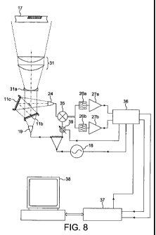
to Figures 8 to 10, the third imaging device differs from the second by using
two
reflecting semiconducting substrates in place of one, which permits an
improved
method of scanning the substrate to be used, as well as other advantages.
The scanning method will first be described. The scene 17 is illuminated with
radiation from Gunn diode oscillator 18. The path for millimetric radiation
returned
from the target 17 is folded because the single high-resistivity silicon
semiconductor
substrate 11 of Figures 5 and 6.is replaced by a pair of high-resistivity
silicon
semiconductor substrates 11 b and 11 c. This has several advantages.
The first advantage is in a simplified method of scanning the reflective spot
over the
image of the scene received back from the lens system 31, 31a. Each of the
semiconductor substrates 11b, l lc is provided with a series of equally spaced
grooves
40. At one end of each substrate, a series of LEDs 41 are provided (Figure
9a), one for
each surface strip 421ying on each side of the grooves 40, the output of which
is
aimed at the surface strip 42. From there it is reflected to the mirror formed
by the
very thin chrome layer 43 at the bottom of the substrate. The result is that
each LED
CA 02682459 2009-09-28
WO 2008/119971 PCT/GB2008/001115
19
41 illuminates, from the underside, the surface of its associated strip 42,
along its
whole length, by virtue of the repeated reflections undergone by the light
from the
LED. Each LED, however, only illuminates the surface of its adjacent strip,
and not
the surface of the others. In fact, an LED is arranged at each end of each
strip, but
only the LED at the left hand end of the strip is shown in Figure 9a. It will
be further
noted that the strips 42 are arranged orthogonally (Figure 10). For example,
the strips
42 might run vertically for the substrate 11 b in Figure 8, and horizontally
for the
substrate 11 c. As shown in Figure 10, the third vertical strip from the near
edge of the
substrate 11 b is illuminated, and the third strip down for the horizontal
strips of the
substrate 11 c is illuminated.
It will be appreciated that the transmitting horn 19 illuminates the scene 17
through
the entire area of the substrate 11b, and that the reflected radiation
impinges on the
entire areas of the substrates 11 b and 11 c. However, the only regions of the
scene that
is received by the horn 24 due illumination of the strips is that area whose
horizontal
extent is determined by the illumination of the third vertical strip on the
substrate 11 b,
and whose vertical extent is determined by the illumination of the third strip
42 on
substrate 1 lc. It will be apparent that the whole area of the scene can be
scanned by
illuminating one horizontal strip and one vertical strip at a time. Thus, for
example,
the scene could be scanned by first illuminating the uppermost horizontal
strip,
together with each of the vertical strips in turn. Then the next uppermost
horizontal
strip could be illuminated, together with each of the vertical strips in turn,
etc.
The scanning is thus simplified compared to using an array of LEDs.
CA 02682459 2009-09-28
WO 2008/119971 PCT/GB2008/001115
The provision of two reflecting substrates, rather than the one of the imaging
devices
of Figures 6 and 8, provides other advantages as well.
In addition to the signal received at the receiving horn 24 due the
illuminated area, the
horn also receives reflections from the whole area of each substrate that
arises from
the change of refractive index at the air/semiconductor interface at the
surface of each
substrate. It has to be borne in mind that the transmitted radiation from the
horn 19 is
plane polarised, and that the radiation reflected from the scene will also be
generally
plane polarised as well. That being the case, it might be thought that this
undesired
reflection could be removed from the received radiation by placing a crossed
polariser
in front of the receiving horn 24, or incorporating a polariser into the horn
itself.
Unfortunately, the reflections at the substrate surfaces introduce some
ellipticity into
the reflections, with the result that the orthogonal component thus introduced
will
pass any such crossed polariser at the horn 24.
The amount of ellipticity introduced depends on the angle of incidence of the
millimetric radiation on the substrate. It is found, following a discovery by
F H Smith,
that the smaller the angle of incidence, the less the amount of ellipticity
introduced.
(Mineralogical Magazine, Vol. 33, March 1964, No. 264, pp725-729). In Figure
8, the
included angle between the substrates l lb, 11 c is 45 , and the angle of
incidence of
the radiation to each substrate is 22.5 . Thus one of the advantages of having
two
reflecting substrates is that it is then possible to introduce less
ellipticity than for the
first two imaging devices, where the angle of incidence is 45 .
CA 02682459 2009-09-28
WO 2008/119971 PCT/GB2008/001115
21
In addition, the grooves 40 result in the substrates 1 lb, l lc forming a pair
of crossed
reflective waveplates, so that the substrates themselves provide the crossed
polarising
action referred to. Radiation falling on substrate 11b in Figure 10 is
reflected as
vertically polarised, and the radiation falling on substrate 11 c is reflected
as being
horizontally polarised. (The radiation reflected from the intersection of the
illuminated strips is not polarised by the substrates). The width of the
strips in a
surface direction at right angles to the direction in which they extend is an
integral
number of half wavelengths of the millimetric radiation, preferably one half
of one
wavelength, and the depth of the grooves 40 is an odd multiple of quarter
wavelengths
of the millimetric radiation, preferably one quarter wavelength in depth. This
depth,
together with the multiple of half-wavelengths strip width, causes the layer
of the
substrate from the face down to the bottom of the grooves to act as a quarter-
wavelength anti-reflection layer. This serves to reduce the strength of the
undesired
elliptical components introduced at the reflections. The quarter-wavelength
depth
results in cancellation of radiation reflected from the surface of the strip
and the
bottom of the groove, and the total volume of the semiconductor material left
in this
layer on each plate is sufficient to reduce the effective refractive index in
the layer to
that of the square root of the refractive index of the base semiconductor
beneath the
grooves, so that the layer acts as a matching layer. The width of the strips
should not
be less than half a wavelength of the millimetric radiation; otherwise the
insertion loss
of the complete device increases rapidly.
The lens system 31, 31a includes a negative element 31a in order to flatten
the field.
to reduce oblique reflections from the non-illuminated regions of the
substrates 11b,
CA 02682459 2009-09-28
WO 2008/119971 PCT/GB2008/001115
22
11 c and therefore differences in polarisation across the complete aperture.
Such an
element could also be provided in the imaging devices of Figures 5 and 6.
The imaging devices of Figures 5, 6 and 8 all have the advantage that coaxial
illumination provides inherent isolation between the illuminating source and
the
receive path, exploiting the known directive capability of an optical beam-
splitter.
This also applies to the double plate design of Figure 8, as well as to the
single plate
designs of Figures 5 and 6. Isolation greater than -50dB is readily achieved;
this is
considerably better than that available from more conventional millimetre-wave
diplexers in microstrip or waveguide. Illumination of the target through the
reflective
means loses about 50% of the incident radiation; this is absorbed in an
orthogonal,
terminated port, and a further loss occurs due to the screening off of the
areas of the
two active scanning strips in the Figure 8 embodiment. For this embodiment, a
typical width for each strip for 250GHz millimetric radiation will be 1.2mm
wide.
Assuming a 40 x 40 array, this gives a total plate size of 60 x 60mm. The
blocking
caused by the two illuminated strips is therefore about 4% of the tota1250GHz
illuminated area, or about 0.2dB extra insertion loss across the whole
aperture of the
imager.
Modifications may, if desired, be made to the imaging devices without
departing from
the scope of the invention. Thus, '/4 wave plates could be used with the
embodiments
of Figures 5 and 6, so as to transmit RH circular polarisation, and to receive
LH
circular. This would reduce the effect of reflections from the non-illuminated
regions
of the substrate 11. These could be placed in front of the transmitting and
receiving
CA 02682459 2009-09-28
WO 2008/119971 PCT/GB2008/001115
23
horns 19, 24, or, indeed, incorporated into those horns, these being aligned
so as to
reduce the elliptical component from the non-illuminated areas of the
substrate.
Less ellipticity would be introduced with the substrates l lb, l lc of the
third imaging
device of Figure 8, and the crossed polarisers could also be placed in front
of, or
incorporated into, the horns 19, 24, and in this case, the substrates could be
plane
without grooves in them. It would be necessary for the scanning of the
illuminated
optical beam to be carried out by some other means, however, such as by the
array of
LEDs 32. Since the unwanted reflections from the non-illuminated areas of the
substrates 11 b, 11 c arise from the rear as well as the front surfaces of the
substrates (a
change in index being present in each case), this could be mitigated by
arranging the
substrate 11 c to be wedge-shaped, so that the reflection from the rear face
due to the
non-illuminated regions is thrown out of the field of view of receiving horn
24.
While the substrates 11b, 11 c may be of similar volume composition of high
resistivity semiconductor to the substrate 11 used in the imaging devices of
Figures 5
and 6, and as described in Figure 4, the substrate may instead comprise a very
thin
layer only of the high-resistivity semiconductor, confined to the strips 42,
(for
example, between 25 m and 5 m, preferably 10 m thick), epitaxially
deposited on
another layer, since the optically excited electron gas creating the
conditions for
reflection, is a close to surface phenomenon. The other layer may be a
transparent
layer with no semiconducting properties. The same arrangement may be used in
Figures 5 and 6, wherein the substrate comprises a thin epitaxially deposited
high
resistivity semiconductor layer as the active layer, and another layer as the
support.
CA 02682459 2009-09-28
WO 2008/119971 PCT/GB2008/001115
24
The imaging devices described may be used for security screening purposes.
However, detection devices are also within the scope of the invention wherein
images
are not formed, but rather the absorption characteristics of a subject are
investigated.
Such devices would tend to operate at higher frequencies, (1011 to 1013 Hz),
and be
narrower beam in order that they could be used at longer ranges. Such could be
modified versions of the imagers of Figures 5 to 8, but where the scanning is
of a
coarse quantisation, for example, eight pixels square. The absorption
characteristics
could be determined by the phase detection described with reference to Figure
7, or
by using as the illuminating source a pair of quantum cascade lasers operating
at
different frequencies. The radiation from the lasers is pulsed. The ratio of
the returned
power at the different frequencies would allow the absorption of the
illuminated
subject to be determined, allowing the detection of items such as explosives.
The
scanning at the substrates is used, not for imaging, but to enable the target
to be
illuminated through the reflective means, as only one pixel will be reflecting
and
therefore blocked to transmission through the reflective means at any one
time. This
allows the use of the same image dissection principles shown in the first
imager,
thereby giving the same improvement to Rayleigh resolution in this device.
Thus, one
set of optics may be used for both transmission of the laser beams and their
return,
thereby providing a cost saving.
Such a narrow beam chemical signature detection could be used in conjunction
with
the imagers described.
At lower, microwave, frequencies, the imagers described could be used in a
guidance
system carried by airborne platform.