Note: Descriptions are shown in the official language in which they were submitted.
CA 02682600 2009-10-01
WO 2008/124424 PCT/US2008/059107
NON-PLANAR CIRCUIT BOARD AND A METHOD FOR FABRICATING
THE SAME
The inventive arrangements relate to methods, systems, and apparatus
for fabricating a non-planar circuit board. More particularly, the present
invention
relates to a method for fabricating a non-planar circuit board comprised of a
liquid
crystal polymer circuit board material or other thermoplastic polymer
material.
Within the government communication market, there is an increasing
push to further miniaturize systems with the use of chip-scale packages, flip-
chip
bonding, and other advances over traditional packaging techniques. Beyond
simple
miniaturization, there is also the desire to integrate circuitry with
structure and
cosmetic packaging to achieve the ability to incorporate electrical functions
within
articles having very different form factors from those that traditionally have
been
used. This goal serves to combine interest in achieving both miniaturization
and full
integration.
There is also a need for a versatile board substrate technology that
provides a reduced dielectric constant over that of conventional board
materials, and
thereby provides means for improving the density of high radio frequency (RF)
circuits. Additionally, for airborne and space applications, there is a need
for a light
board material that can also play a role in providing mechanical structure.
Liquid crystal polymer (LCP) materials are relatively light, ultra-thin
materials that can permanently mold to any shape. LCP materials also have
relatively
low moisture and oxygen permeability characteristics as compared to
conventional
circuit board materials. As such, LCP materials are suitable for making thin,
multi-
layer circuit boards as well as highly detailed, high performance planar
circuit boards.
LCP materials are also suitable for making three-dimensional (3D) micro-
electro-
mechanical circuits. LCP materials are further suitable for making circuit
boards
intended for extreme temperature applications and/or intense radiation
applications.
The invention concerns a method for forming a circuit board. The
method includes forming a circuit board substrate from a circuit board
material. The
method also includes positioning the circuit board substrate on a rigid
structure having
-1-
CA 02682600 2009-10-01
WO 2008/124424 PCT/US2008/059107
a three dimensional contoured surface. The method further includes applying
heat
and applying pressure to the circuit board substrate to at least partially
conform the
circuit board substrate to the three dimensional contoured surface.
According to an aspect of the invention, the method includes disposing
a circuit pattern on the circuit board substrate prior to the steps of
applying heat and
applying pressure to the circuit board substrate. Alternatively, the method
includes
disposing a circuit pattern on the circuit board substrate after the steps of
applying
heat and applying pressure to the circuit board substrate.
According to another aspect of the invention, the method includes
selecting the circuit board substrate to have a planar configuration. The
method also
includes selecting the circuit board material to be a thermoplastic polymer
material,
such as a liquid crystal polymer material. The thermoplastic polymer material
includes a single sheet of circuit board material or two or more layers of
circuit board
material.
According to another aspect of the invention, the method includes
removing the circuit board substrate from the three dimensional contoured
surface
after applying heat and applying pressure to the circuit board substrate. In
this regard,
it should be appreciated that a release agent may be optionally disposed
between the
circuit board substrate and the three dimensional contoured surface prior to
positioning the circuit board substrate on a rigid structure. The release
agent is
selected from the group consisting of a film, a liner, a lubricant, and a wax.
According to another embodiment of the invention, the method
includes permanently adhering the circuit board substrate to the three
dimensional
contoured surface in the steps of applying heat and applying pressure to the
circuit
board substrate. In this regard, it should be appreciated that an adhesive
agent can be
disposed between the circuit board substrate and the three dimensional
contoured
surface prior to positioning the circuit board substrate on a rigid structure.
Alternatively, at least one of the circuit board material and a material
forming the
three dimensional contoured surface is selected to produce an adhesive bond
between
-2-
CA 02682600 2009-10-01
WO 2008/124424 PCT/US2008/059107
the circuit board material and the three dimensional contoured surface in the
steps of
applying heat and applying pressure to the circuit board substrate.
The method includes positioning the circuit board substrate and the
rigid structure in an interior volume at least partially defined by a vacuum
bag. The
method also includes creating a pressure differential comprising a reduced
pressure
within the interior volume relative to an environment external to the interior
volume.
This pressure differential can be created by evacuating at least a portion of
a gas
contained in the interior volume. This pressure differential can also be
created or
enhanced by positioning the circuit board substrate and the rigid structure in
a
pressure chamber, and increasing a pressure in the pressure chamber. The
method
further includes increasing the pressure differential after applying heat to
the circuit
board substrate. According to another aspect of the invention, the step of
applying
heat to the circuit board substrate further includes equilibrating the circuit
board
substrate at a temperature prior to increasing the pressure. The temperature
is selected
to be less than a temperature of a melting point of the circuit board
material.
According to yet another aspect of the invention, the method includes
selecting the rigid structure to include a tool and a part releasably disposed
on the
tool. The method also includes permanently bonding the part to the circuit
board
substrate. The method further includes removing from the tool the circuit
board
substrate with the part permanently bonded thereto after applying heat and
applying
pressure to the circuit board substrate.
Embodiments will be described with reference to the following
drawing figures, in which like numerals represent like items throughout the
figures,
and in which:
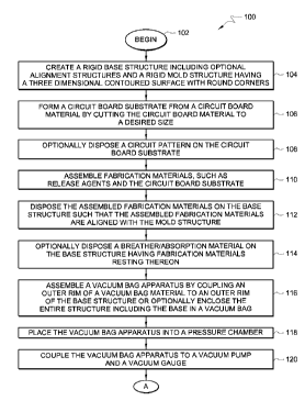
FIG. lA-1C are collectively a flow diagram of a method for fabricating
a circuit board that is useful for understanding the invention.
FIG. 2 is a perspective view of a rigid base structure that is useful for
understanding the present invention.
FIG. 3 is a cross-sectional view of a projecting relief taken along line
3-3 of FIG. 2.
-3-
CA 02682600 2009-10-01
WO 2008/124424 PCT/US2008/059107
FIG. 4 is a perspective view of a circuit board substrate that is useful
for understanding the present invention.
FIG. 5 is a schematic illustration of fabrication materials being
disposed on the rigid base structure of FIG. 2 that is useful for
understanding the
present invention.
FIG. 6 is a side view of fabrication materials disposed on the rigid base
structure shown in FIG. 2 that is useful for understanding the present
invention.
FIG. 7 is a side view of a breather/absorption material disposed on the
base structure having fabrication materials disposed thereon that is useful
for
understanding the present invention.
FIG. 8 is a side view of an assembled vacuum bag material apparatus
that is useful for understanding the invention.
FIG. 9 is a side view of the vacuum bag apparatus disposed in a
pressure chamber that is useful for understanding the invention.
FIG. 10 is a side view of the vacuum bag apparatus coupled to a
vacuum pump and a vacuum gauge that is useful for understanding the invention.
FIG. 11 is a side view of an at least partially evacuated vacuum bag
apparatus that is useful for understanding the invention.
FIG. 12 is a side view of at least partially evacuated vacuum bag
apparatus having an increased temperature applied thereto that is useful for
understanding the invention.
FIG. 13 is a side view of the vacuum bag apparatus having an
increased pressure applied thereto that is useful for understanding the
invention.
FIG. 14 is a side view of the vacuum bag apparatus removed from the
pressure chamber that is useful for understanding the invention.
FIG. 15 is a side view of a partially disassembled vacuum bag
apparatus that is useful for understanding the present invention.
FIG. 16 is a side view of the fabrication materials including a non-
planar circuit board substrate removed from the vacuum bag apparatus that is
useful
for understanding the present invention.
-4-
CA 02682600 2009-10-01
WO 2008/124424 PCT/US2008/059107
FIG. 17 is a side view of a projecting relief permanently bonded to a
circuit board substrate that is useful for understanding the present
invention.
An embodiment of the present invention will now be described with
respect to FIG. 1 through FIG. 17. Some embodiments of the present invention
provide methods, systems, and apparatus relating to the fabrication of a non-
planar
circuit board. Such methods, systems, and apparatus also relate to the
fabrication of a
non-planar circuit pattern disposed on a circuit board substrate. The present
invention
further relates to methods, systems, and apparatus relating to the fabrication
of a
multi-layer, non-planar circuit board having defect-free interconnects.
Referring now to FIG. lA, there is provided a flow diagram of a
method 100 for fabricating a circuit board that is useful for understanding
the
invention. As shown in FIG. 1, the method 100 begins with step 102 and
continues
with step 104. In step 104, a rigid base structure is created. The rigid base
structure
is formed of a rigid material suitable to withstand relatively high
temperature and
pressures. Such rigid materials include, but are not limited to, copper,
aluminum, and
steel. The rigid base structure can also be formed of a non-stick material,
such as
Teflon available from E. I. Du Pont De Nemours and Company, of Wilmington,
Delaware. A perspective view of a rigid base structure 200 is provided in FIG.
2.
As shown in FIG. 2, the rigid base structure 200 can be comprised of
alignment structures 2021-2024. The alignment structures 2021-2024 can
advantageously be provided when a registration is required between fabrication
materials and a rigid mold structure 204. The rigid mold structure 204 may be
optionally fixed to the rigid base structure 200 or engaged by two or more of
the
alignment structures 2021-2024. The rigid mold structure 204 has a three
dimensional
(3D) contoured surface 206 to which fabrication materials conform when heat
and
pressure are applied thereto. The 3D contoured surface 206 can include a
projecting
relief 208 and/or a hollow relief 210.
A cross sectional view of the projecting relief 208 is provided in FIG.
3. As shown in FIG. 3, the projecting relief 208 is advantageously designed to
include corners 302i, 3 022 and walls 304i, 3 042. The corners 302i, 3 022
have a radius
-5-
CA 02682600 2009-10-01
WO 2008/124424 PCT/US2008/059107
selected in accordance with a particular rigid mold structure 304 application.
For
example, the corners 3021, 3022 have a radius suitable for offsetting severe
elongation
of a circuit pattern at the corners 302i, 3022 when heat and pressure are
applied to a
circuit board substrate. As will be appreciated by a person skilled in the
art, severe
elongation of a cladding material disposed on a circuit board substrate can
cause an
undesirable circuit pattern failure (i.e., damage and cracking of a cladding
material).
As such, each corner 302i, 3022 preferably has at least one (1) millimeter
(mm) to
three (3) millimeter (mm) radius for preventing damage to a circuit pattern
when heat
and pressure are applied thereto. Still, the invention is not limited in this
regard.
As shown in FIG. 3, the walls 304i, 3042 are non-vertical walls
designed for providing a uniform elongation of a circuit pattern along the
walls 304i,
3042 when heat and pressure are applied to a circuit board substrate. In this
regard, it
should be appreciated that the projecting relief 208 is designed with wall
angles 3 101,
3102 substantially less than ninety degrees (90 ). Still, the invention is not
limited in
this regard.
As will be understood by a person skilled in the art, the wall angles
310i, 3102 can be defined by a mathematical Equation (1), under the assumption
that
the elongation of the substrate and cladding occurs predominantly along the
length of
the walls 304i, 3042.
OmaX = cos 1 (100% / (EL + 100%)) (1)
where Bm,,x is the maximum angle value for the wall angles 310i, 3102. EL is
the
elongation to break limit in percent for a cladding material disposed on a
circuit board
substrate (described below in relation to FIG. 3).
For example, elongation to break limits (ELs) for a copper cladding
material are listed in Table 1.
-6-
CA 02682600 2009-10-01
WO 2008/124424 PCT/US2008/059107
TABLE 1
ELECTRODEPOSITED (ED) COPPER ROLLED COPPER
WEIGHT THICKNESS ELONGATION WEIGHT THICKNESS ELONGATION
(ounce) (micrometers) LIMIT (percent) (ounce) (micrometers) LIMIT (percent)
0.5 oz 17.0 um 20.0% 0.5 oz 17.0 um 8.0%
1.0 oz 34.0 um 28.0% 1.0 oz 34.0 um 13.0%
2.0 oz 68.0 um 42.0% 2.0 oz 68.0 um 27.0%
By substituting the above listed EL values into Equation (1), the maximum
angle
values BmaX for the wall angles 310i, 3102 of a projecting relief 208 to be
used in
fabricating a non-planar circuit board with the above listed copper cladding
materials
can be calculated. These calculated maximum angle values BmaX are listed in
Table 2.
It should be understood that it is preferred to restrain the wall angle by
design to an
angle much less than the limit value, BmaX, so that the elongation is
preferably held to
less than one half (1/2) the elongation to break limit and more preferably to
less than
one fourth (1/4) the elongation to break limit as determined by the
mathematical
Equation (1).
TABLE 2
COPPER EL OF Oõ1a~, FOR EL OF Oõ1a~, FOR
WEIGHT ED COPPER ED COPPER ROLLED COPPER ROLLED COPPER
(ounce) (percent) (degrees) (percent) (degrees)
0.5 oz 20.0% 33.6 8.0% 22.2
1.0 oz 28.0% 38.6 13.0% 27.8
2.0 oz 42.0% 45.2 27.0% 38.1
Referring again to FIG. lA, the method 100 continues with step 106
where a circuit board substrate is formed from a circuit board material. This
step can
involve cutting a circuit board material to a desired shape and size. This
step can also
-7-
CA 02682600 2009-10-01
WO 2008/124424 PCT/US2008/059107
involve forming alignment apertures in the circuit board material. A
perspective view
of a circuit board substrate 400 is provided in FIG. 4.
As shown in FIG. 4, the circuit board substrate 400 is comprised of
optional alignment apertures 4021-4024. The alignment apertures 4021-4024 are
formed in the circuit board substrate using any means known in the art, such
as a
drilling means or a hole punching means. The alignment apertures 4021-4024 are
sized and shaped for receiving the optional alignment structures 202i-2024
described
above in relation to FIG. 2.
According to an aspect of the invention, the circuit board substrate 400
is comprised of a liquid crystal polymer (LCP) or other thermoplastic polymer
circuit
board material. For example, the circuit board material can be an R/flex 3000
circuit board material available from Rogers Corporation, of Rogers,
Connecticut.
According to another aspect of the invention, the circuit board substrate 400
is
comprised of a single layer clad circuit board material, a single layer unclad
circuit
board material, a multi-layer (or laminate) clad circuit board material, or a
multi-layer
(or laminate) unclad circuit board material. Still, the invention is not
limited in this
regard.
Referring again to FIG. lA, the method 100 continues with step 110
where a circuit pattern is optionally disposed on the circuit board substrate
400 using
any technique known in the art. Such techniques include, but are not limited
to,
etching techniques, inkjet printing technique, and silk screening techniques.
After
step 110, step 112 is performed where fabrication materials are assembled. A
side
view of assembled fabrication materials 502 is provided in FIG. 5.
As shown in FIG. 5, the fabrication materials include the circuit board
substrate 400 and/or one or more release agents 504i, 5042. The release agent
5042 is
advantageously provided to prevent adhesion of the circuit board substrate 400
to the
base structure 200 when heat and pressure are applied thereto. Similarly, the
release
agent 504, is provided to prevent adhesion of a breather/absorption material
(described below in relation to FIG. 7) to the fabrication materials 502 when
heat and
pressure are applied thereto. The release agents 504i, 5042 include, but are
not
-8-
CA 02682600 2009-10-01
WO 2008/124424 PCT/US2008/059107
limited to, films, wax sheets and release liners. For example, the release
agent may
consist of a Teflon liner. Alternatively, a low surface energy release film
may be
applied to the circuit board substrate 400 or a surface of the mold structure
204.
Referring again to FIG. lA, the method continues with step 112. In
step 112, the assembled fabrication materials 502 are disposed on the base
structure
200 such that the fabrication materials 502 are aligned with the mold
structure 204. A
schematic illustration of assembled fabrication materials 502 being disposed
on the
rigid base structure 200 is provided in FIG. 5. A schematic illustration of
the
assembled fabrication materials 502 disposed on the rigid base structure 200
is
provided in FIG. 6.
After step 112, step 114 is performed where a breather/absorption
material is optionally disposed on the rigid base structure 200 having the
fabrication
materials 502 resting thereon. A side view of a breather/absorption
materia1702
disposed on the fabrication materials 502 and the base structure 200 is
provided in
FIG. 7. As will be appreciated by a person skilled in the art, the
breather/absorption
materia1702 is provided for ensuring uniform vacuum pressure across the
fabrication
materials 502 when heat and pressure are applied thereto. The
breather/absorption
materia1702 is also provided for absorbing excess resin from a multi-layer (or
laminate) circuit board substrate 400. Breather/absorption materials are well
known
to persons skilled in the art. Thus, the breather/absorption materia1702 will
not be
described in detail herein. However, it should be appreciated that any
breather/absorption material known in the art can be used without limitation.
As shown in FIG. lA, the method 100 continues with step 116. In step
116, a vacuum bag apparatus is assembled. A side view of an assembled vacuum
bag
apparatus 800 is provided in FIG. 8. As shown in FIG. 8, the vacuum bag
apparatus
800 is comprised of a vacuum bag materia1802 disposed on the
breather/absorption
materia1702. The vacuum bag materia1802 is a flexible dimensionally stable
film,
such as Kapton available from E. I. Du Pont De Nemours and Company, of
Wilmington, Delaware. The vacuum bag material 802 forms a seal with the base
structure 200. For example, an outer rim 808 of the vacuum bag materia1802 is
-9-
CA 02682600 2009-10-01
WO 2008/124424 PCT/US2008/059107
coupled to an outer rim 812 of the base structure 200 with a sealant means
810. The
sealant means includes, but is not limited to, a mechanical connector means,
sealant
tape, epoxy, adhesive, and/or glue.
Referring again to FIG. lA, the method 100 continues with a step 118.
In step 118, the vacuum bag apparatus 800 is placed in a pressure chamber. A
schematic illustration of the vacuum bag apparatus 800 disposed in a pressure
chamber 900 is provided in FIG. 9. In this regard, it should be appreciated
that the
pressure chamber 900 is a container in which heat and pressure are applied to
materials disposed therein.
According to an embodiment of the invention, the pressure chamber
900 is an autoclave. The autoclave can be selected as an autoclave in which
temperature and pressure sequences can be software defined and pre-programmed
into
a memory of the autoclave. For example, the autoclave is an Econoclave
available
from ASC Process Systems, of Sylmar, California. Still, the invention is not
limited
in this regard.
Referring again to FIG. lA, the method 100 continues with step 120
where the vacuum bag apparatus 800 is coupled to a vacuum pump and a vacuum
gauge. As will be understood by a person skilled in the art, a leak free
connection
between the vacuum bag apparatus 800 and each of the listed devices is
necessary for
forming a non-planar circuit board substrate by applying a defined amount of
pressure
thereto. A schematic illustration of the vacuum bag apparatus 800 coupled to a
vacuum pump 1002 and a vacuum gauge 1004 is provided in FIG. 10.
As shown in FIG. 10, a coupling means 1006 is provided for coupling
the vacuum bag materia1802 to a vacuum pump 1002. As will be understood by a
person skilled in the art, the vacuum pump 1002 is provided for selectively
reducing a
pressure in an interior volume of the vacuum bag material 802 by evacuating at
least a
portion of a gas contained therein. The coupling means 1006 is comprised of a
tubular conduit 1008 and a connector means 1010. The tubular conduit 1008 is
selected in accordance with a particular vacuum bag apparatus 800 application.
For
example, the tubular conduit 1008 is selected as a flexible tube-like
structure formed
-10-
CA 02682600 2009-10-01
WO 2008/124424 PCT/US2008/059107
of a material suitable to withstand high temperatures and pressures. The
connector
means 1010 is configured to maintain a leak-free seal between the vacuum bag
materia1802 and the tubular conduit 1008 at high temperatures and pressures.
For
example, the connector means 1010 is comprised of a top bolt, a seal ring, and
a
threaded valve base having a vacuum feed through aperture. Still, the
invention is not
limited in this regard.
A coupling means 1012 is also provided for coupling the vacuum bag
materia1802 to a vacuum gauge 1004. As will be understood by a person skilled
in
the art, a vacuum gauge is provided for tracking pressures inside the vacuum
bag
apparatus 800. The coupling means 1012 is comprised of a tubular conduit 1014
and
a connector means 1016. The tubular conduit 1014 is selected in accordance
with a
particular vacuum bag apparatus 800 application. For example, the tubular
conduit
1014 is selected as a flexible tube-like structure formed of a material
suitable to
withstand high temperatures and pressures. The connector means 1016 is
configured
to maintain a leak free seal between the tubular conduit 1014 and the vacuum
bag
materia1802 at the high temperatures and pressures. For example, the connector
means 1016 is comprised of a top bolt, a seal ring, and a threaded valve base
having a
vacuum feed through aperture. Still, the invention is not limited in this
regard.
Referring again to FIG. 1B, the method 100 continues with step 122 of
FIG. lB. In step 122, a pressure differential is created by reducing pressure
within the
vacuum bag apparatus 800 relative to an environment external to the vacuum bag
apparatus 800. This step can involve evacuating at least a portion of a gas
contained
in the interior volume of the vacuum bag apparatus 800. According to an
embodiment of the invention, a gas contained in the interior volume of the
vacuum
bag apparatus 800 is evacuated to a vacuum gauge 106 pressure of less than
negative
seven hundred forty millimeters of mercury (-740 mm Hg). Still, the invention
is not
limited in this regard.
A schematic illustration of an at least partially evacuated vacuum bag
apparatus 800 is provided in FIG. 11. As shown in FIG. 11, at least a portion
of a gas
contained in the interior volume 1102 of the vacuum bag apparatus 800 has been
-11-
CA 02682600 2009-10-01
WO 2008/124424 PCT/US2008/059107
evacuated through use of the vacuum pump 1002. As such, a pressure within the
interior volume 1102 is reduced. In effect, a pressure differential is created
between a
pressure in the interior volume 1102 and a pressure in an environment external
1104
to the vacuum bag apparatus 800.
Referring again to FIG. 1B, the method 100 continues with step 124.
In step 124, a test is optionally performed to determine whether there are
leaks in the
vacuum bag apparatus 800. Such tests are well known to persons skilled in the
art.
Thus, the test to determine whether there are leaks in the vacuum bag
apparatus 800
will not be described in great detail herein. However, it should be
appreciated that
any test known in the art that is suitable for determining whether there are
leaks in the
vacuum bag apparatus 800 can be used without limitation.
After step 124, the method 100 continues with a decision step 126. If
there are leaks in the vacuum bag apparatus 800, then step 128 is performed
where the
method 100 ends. However, if the vacuum bag apparatus 800 is absent of leaks,
then
step 130 is performed. In step 130, heat is applied to the vacuum bag
apparatus 800
for at least partially conforming a circuit board substrate 400 to a three
dimensional
(3D) contoured surface 206 of a mold structure 204. This step involves
equilibrating
the circuit board substrate 400 at a temperature which is substantially less
than a
temperature of a melting point of a circuit board material forming the circuit
board
substrate 400. In this regard, it should be appreciated that the temperature
applied to a
circuit board material comprising the single sheet or multilayer laminate is
preferably
fifty to eighty percent (50-80 %), more preferably fifty to seventy percent
(50-70%),
or most preferably fifty to sixty-five percent (50-65%) of a melting point
temperature
of the lowest melting component of the circuit board materials. A side view of
the
vacuum bag apparatus 800 having an increased temperature applied thereto is
provided in FIG. 12.
According to an embodiment of the invention, a circuit board substrate
116 is selected as R/flex 3000 circuit board material available from Rogers
Corporation, of Rogers, Connecticut. A temperature of a melting point for a
bondply
material (e.g., R/flex 3908) disposed in the R/flex 3000 circuit board
material
-12-
CA 02682600 2009-10-01
WO 2008/124424 PCT/US2008/059107
system is approximately two hundred ninety degrees Celsius (290 C). A
temperature
of a melting point for a core material (R/flex 3850) disposed in the R/flex
3000
circuit board material is three-hundred fifteen degrees Celsius (315 C). As
such, a
temperature of an environment external to a vacuum bag apparatus 800 is
selectively
increased from room temperature to two hundred eighteen degrees Celsius (218
C) at
a relatively high ramp rate. Subsequently, the temperature external of an
environment
external to a vacuum bag apparatus 800 is selectively increased from two
hundred
eighteen degrees Celsius (218 C) to two hundred twenty-seven degrees Celsius
(227
C) at a relatively low ramp rate thereby equilibrating the circuit board
substrate 400 at
a temperature which is substantially less than a temperature of a melting
point of a
circuit board material, i.e., two hundred ninety degrees Celsius (290 C) and
three-
hundred fifteen degrees Celsius (315 C). With regard to preserving the
integrity of
optionally included patterned copper cladding, it is preferable to employ a
maximum
temperature within the enclosure 900 that is the lowest possible temperature
consistent with obtaining a desired accuracy between a topology of a molded
part and
a surface of the too1206. Thus, a temperature (e.g., 190 C) near a bottom of
a
suggested range is preferred when it is necessary to preserve the integrity of
a finely
patterned cladding. Still, the invention is not limited in this regard.
Referring again to FIG. 1B, the method 100 continues with a step 132
where the pressure differential is increased to fully conform the circuit
board substrate
400 to the three dimensional (3D) contoured surface 206 of the mold structure
204.
This step can involve increasing a pressure in the environment external 1104
to the
vacuum bag apparatus 800. According to an embodiment of the invention, a
pressure
in the environment external 1104 to the vacuum bag apparatus 800 is increased
to one
hundred pounds per square inch (100 psi). Still, the invention is not limited
in this
regard.
A side view of the vacuum bag apparatus 800 having an increased
pressure applied thereto is provided in FIG. 13. As shown in FIG. 13, the
circuit
board substrate 400 is fully conformed to the three dimensional (3D) contoured
surface 206 of the mold structure 204.
-13-
CA 02682600 2009-10-01
WO 2008/124424 PCT/US2008/059107
Referring again to FIG. 1B, the method 100 continues with a decision
step 134. If a defined period of time has not expired, then the method 100
continues
tracking the amount of time that has passed since the performance of step 132.
However, if the defined period of time has lapsed, then the method 100
continues with
step 136 of FIG. 1C.
In step 136, the temperature of the environment external 1104 to the
vacuum bag apparatus 800 is decreased. For example, the temperature of the
environment external 1104 is decreased from two hundred twenty-seven degrees
Celsius (227 C) to twenty-one degrees Celsius (21 C). In effect, the circuit
board
substrate 400 is cooled such that it permanently retains it non-planar shape
when
removed from the bag apparatus 800. In this regard, it should be appreciated
that
methods for decreasing a temperature of the environment external 1104 to the
vacuum
bag apparatus 800 are well known to persons skilled in the art. Any such
method can
be used without limitation.
Referring again to FIG. 1C, the method 100 continues with a step 138.
In step 138, the pressure differential is decreased by reducing a pressure
external to
the vacuum bag apparatus 800. This step can involve decreasing the pressure of
the
pressure chamber 900. In this regard, it should be appreciated that methods
for
decreasing the pressure of the pressure chamber 900 are well known to persons
skilled
in the art. Any such method can be used without limitation.
After decreasing the pressure differential, the method continues with
step 140 where the vacuum bag apparatus 800 is removed from the pressure
chamber
900. A schematic illustration of the vacuum bag apparatus 800 removed from the
pressure chamber 900 is provided in FIG. 14. In step 142, the vacuum bag
material
802 and the optional breather/absorption materia1702 are removed from the
vacuum
bag apparatus 800 as shown in FIG. 15. Thereafter, the fabrication materials
502 are
removed from the three dimensional (3D) contoured surface 206 of the mold
structure
204 as shown in FIG. 16. In step 132, a circuit pattern is optionally disposed
on the
non-planar circuit board substrate 400. After step 132, step 134 is performed
where
the method 100 ends.
-14-
CA 02682600 2009-10-01
WO 2008/124424 PCT/US2008/059107
A person skilled in the art will appreciate that the method 100 is one
embodiment of a method for forming a non-planar circuit board. However, the
invention is not limited in this regard and any other method for forming a non-
planar
circuit board can be used without limitation. For example, the method 100 can
also
include disposing a thermocouple monitor in the vacuum bag apparatus 800 or
the
pressure chamber 900 for reading and logging temperatures in close proximity
to the
circuit board substrate 400 when heat and pressure are applied thereto. The
method
100 can further include securing a part, such as a heat spreader or a heat
sink, in a
well or cavity formed in the circuit board substrate 400.
According to one alternative embodiment of the invention, a circuit
board substrate is permanently adhered to a portion of a three dimensional
contoured
surface. In this regard, it should be appreciated that this adhesion can be
formed by
applying heat and pressure to the circuit board substrate disposed on the
three
dimensional contoured surface. In such a scenario, a circuit board material
and/or a
material forming the three dimensional contoured surface can be selected to
produce
an adhesive bond between the same when heat and pressure are applied thereto.
For
example, such circuit board materials include, but are not limited to, a
liquid crystal
polymer (LCP) or other thermoplastic polymer circuit board material. Such
materials
forming the three dimensional contoured surface include, but are not limited
to,
copper, aluminum, and steel. Alternatively, this adhesion can be formed with
an
adhesive or glue after heat and pressure are applied to the he circuit board
substrate
and the three dimensional contoured surface. An illustration of the projecting
relief
208 permanently coupled to the circuit board substrate 400 is shown in FIG.
17. Still,
the invention is not limited in this regard.
According to yet another alternative embodiment of the invention, the
method 100 includes selecting the rigid base structure 200 to be a tool. The
method
100 also includes selecting the projecting relief 208 to be a part, such as a
heat
spreader or a heat sink. The method 100 further includes releasably disposing
the part
on the tool and permanently coupling the part to the circuit board substrate
400 by
applying heat and pressure thereto. Subsequently, the circuit board substrate
400 is
-15-
CA 02682600 2009-10-01
WO 2008/124424 PCT/US2008/059107
removed from the too1200 with the part 208 permanently bonded thereto. An
illustration of the circuit board substrate 400 removed from the too1200 with
the part
208 permanently bonded thereto is provided in FIG. 17. Still, the invention is
not
limited in this regard.
The following Examples are provided in order to further illustrate the
present invention. The scope of the invention, however, is not to be
considered
limited in any way thereby.
EXAMPLE 1
A liquid crystal polymer (LCP) is selected as an R/flex 3850 LCP
core circuit board material available from Rogers Corporation, of Rogers,
Connecticut. The LCP core circuit board material is subjected to an etching
process
to remove both sides of its two-side electrodeposited copper cladding
therefrom. A
rigid mold structure (i.e., an embossing tool) having a raised plateau region
is
machined from aluminum. The raised plateau region is raised above a
surrounding
region by seventy five hundredths of a millimeter (0.75 mm).
A stack-up is formed by disposing the rigid mold structure on a rigid
base structure, the LCP core circuit board material on the rigid mold
structure, a
release agent on the LCP core circuit board material, and a
breather/absorption
material on the release agent. Thereafter, the stack-up is placed in a vacuum
bag
consisting of polyimide film. The vacuum bag is sealed to the rigid base
structure
with a vacuum sealing tape thereby forming a vacuum bag apparatus. The vacuum
sealing tape is selected as AVBS750 available from Airtech International Inc.,
of
Huntington Beach, California.
The vacuum bag apparatus is placed within an autoclave and a heat and
pressure cycle is initiated. The heat and pressure cycle consists of ramping a
temperature of the autoclave to two hundred thirty-two degrees Celsius (232
C).
Once the temperature of the autoclave reaches two hundred thirty-two degrees
Celsius
(232 C), a pressure of the autoclave is ramped to seven tenths of a mega
Pascal (0.70
MPa). A soak time of one hour (1 hr) at two hundred thirty-two degrees Celsius
(232
-16-
CA 02682600 2009-10-01
WO 2008/124424 PCT/US2008/059107
C) and seven tenths of a mega Pascal (0.70 MPa) is performed. After one hour
(1 hr),
the temperature and pressure of the autoclave are reduced. Thereafter, the
vacuum
bag apparatus is removed from the autoclave. Also, the LCP core circuit board
material is removed from the vacuum bag apparatus.
It should be appreciated that the LCP core circuit board material has no
deterioration, such as light penetrating through thinned/punctured regions of
the LCP
core circuit board material. Additionally, the molded LCP core circuit board
material
is stable in a standard reflow oven environment up to two hundred ten degrees
Celsius
(210 C), i.e., an embossed region of the LCP core circuit board does not
experience
dimensional changes toward an original planar geometry.
EXAMPLE 2
A liquid crystal polymer (LCP) core circuit board material is selected
as an R/flex 3850 LCP core circuit board material available from Rogers
Corporation, of Rogers, Connecticut. The LCP core circuit board material is
comprised of an electrodeposited copper cladding having a half an ounce (0.50
oz)
weight and a seventeen micrometer (17 m) thickness. The LCP core circuit
board
material is subjected to an etching process to remove one (1) side of its two-
side
copper cladding therefrom. The other side of its two-side copper cladding is
subjected to an etching process to form a circuit pattern having an array of
interconnects suitable for mounting a chip. The array is comprised of bond
pads
connected by a series of traces. The traces are selected to have widths of
fifty
micrometers (50 m), sixty-two and a half micrometers (62.50 m), and one
hundred
twenty five micrometers (125 m).
A rigid mold structure having a raised plateau region is machined from
aluminum. The raised plateau region is raised above a surrounding region by
approximately sixty three hundredths of a millimeter (0.63 mm). A stack-up is
formed by disposing the rigid mold structure on a rigid base structure, the
LCP core
circuit board material on the rigid mold structure, a release agent on the LCP
core
circuit board material, and a breather/absorption material on the release
agent.
-17-
CA 02682600 2009-10-01
WO 2008/124424 PCT/US2008/059107
Thereafter, the stack-up is placed in a nylon vacuum bag. The nylon vacuum bag
is
selected as Wrightlon TM Folien WL8400 available from Airtech International
Inc., of
Huntington Beach, California. The vacuum bag is sealed to the rigid base
structure
with a vacuum sealing tape thereby forming a vacuum bag apparatus. The vacuum
sealing tape is selected as GS213-3 available from Airtech International Inc.,
of
Huntington Beach, California.
The vacuum bag apparatus is placed within an autoclave and a heat and
pressure cycle is initiated. The heat and pressure cycle consists of ramping a
temperature of the autoclave to two hundred thirty-two degrees Celsius (232
C).
Once the temperature of the autoclave reaches two hundred thirty-two degrees
Celsius
(232 C), a pressure of the autoclave is ramped to seven tenths of a mega
Pascal (0.70
MPa). A soak time of one hour (1 hr) at two hundred thirty-two degrees Celsius
(232
C) and seven tenths of a mega Pascal (0.70 MPa) is performed. After one hour
(1 hr),
the temperature and pressure of the autoclave are reduced. Thereafter, the
vacuum
bag apparatus is removed from the autoclave. Also, the LCP core circuit board
material is removed from the vacuum bag apparatus.
It should be appreciated that the LCP core circuit board material has no
evidence of deterioration, such as light penetrating through thinned/punctured
regions
of the LCP core circuit board material. However, it should also be appreciated
that
the required elongation to break limit (EL) of the copper traces is near the
limit for
half an ounce (0.50 oz) electrodeposited copper, i.e., approximately a twenty
percent
(20 %) EL. As a result, a few traces experienced breaks.
EXAMPLE 3
A liquid crystal polymer (LCP) core circuit board material is selected
as an R/flex 3850 LCP core circuit board material available from Rogers
Corporation of Rogers, Connecticut. The LCP core circuit board material is
comprised of an electrodeposited copper cladding having a half an ounce (0.50
oz)
weight and a seventeen micrometer (17 m) thickness. The LCP core circuit
board
material is subjected to an etching process to remove one (1) side of its two-
side
-18-
CA 02682600 2009-10-01
WO 2008/124424 PCT/US2008/059107
copper cladding therefrom. The other side of its two-side copper cladding is
subjected to an etching process to form a circuit pattern having an array of
interconnects suitable for mounting a chip. The array is comprised of bond
pads
connected by a series of traces. The traces are selected to have widths of
fifty
micrometers (50 m), sixty-two and a half micrometers (62.50 m), and one
hundred
twenty five micrometers (125 m).
A rigid mold structure having a raised plateau region is machined from
aluminum. The raised plateau region is raised above a surrounding region by
approximately sixty three hundredths of a millimeter (0.63 mm). A stack-up is
formed by disposing the rigid mold structure on a rigid base structure, the
LCP core
circuit board material on the rigid mold structure, a release agent on the LCP
core
circuit board material, and a breather/absorption material on the release
agent.
Thereafter, the stack-up is placed in a nylon vacuum bag. The nylon vacuum bag
is
selected as Wrightlon TM Folien WL8400 available from Airtech International
Inc., of
Huntington Beach, California. The vacuum bag is sealed to the rigid base
structure
with a vacuum sealing tape thereby forming a vacuum bag apparatus. The vacuum
sealing tape is selected as GS213-3 available from Airtech International Inc.,
of
Huntington Beach, California.
The vacuum bag apparatus is placed within an autoclave and a heat and
pressure cycle is initiated. The heat and pressure cycle consists of ramping
the
temperature of the autoclave to one hundred ninety degrees Celsius (190 C)
under a
pressure equal to atmospheric pressure that is created by vacuum evacuation of
the
bag. A soak time of one hour (1 hr) at one hundred ninety degrees Celsius (190
C) is
performed. After one hour (1 hr), the temperature and pressure of the
autoclave are
reduced. Thereafter, the vacuum bag apparatus is removed from the autoclave.
Also,
the LCP core circuit board material is removed from the vacuum bag apparatus.
It should be appreciated that the LCP core circuit board material has no
evidence of deterioration, such as light penetrating through thinned/punctured
regions
of the LCP core circuit board material. The temperature and vacuum are
sufficient
enough to form the LCP material to the shape of the mold without breaking any
of the
-19-
CA 02682600 2009-10-01
WO 2008/124424 PCT/US2008/059107
fine circuit line traces, which suggests that the elongation limit of the
copper traces
has not been exceeded.
EXAMPLE 4
A multi-step approach is implemented to arrive at an embossed
multilayer laminate circuit board material. First, two (2) fifty micrometer
(50 m)
liquid crystal polymer (LCP) core circuit board materials are selected as
R/flex 3850
available from Rogers Corporation, of Rogers, Connecticut. Each of the LCP
core
circuit board materials are subjected to an etching process to remove both
sides of a
two-side electrodeposited copper cladding therefrom. Subsequently, the LCP
core
circuit board materials are laminated together by disposing a fifty micrometer
(50 m)
bonding film between the LCP core circuit board materials. The bonding film is
selected as R/flex 3908 available from Rogers Corporation, of Rogers,
Connecticut.
The laminated LCP core circuit board material is disposed in a vacuum bag
apparatus.
The vacuum bag apparatus is disposed in an autoclave and a heat and pressure
cycle is
initiated. The heat and pressure cycle consists of immediately applying a
pressure of
one and a fourth mega Pascals (1.40 MPa) to the vacuum bag apparatus. The heat
and
pressure cycle also consists of ramping a temperature of the autoclave to two
hundred
ninety-six degrees Celsius (296 C).
Thereafter, a rigid mold structure having a raised plateau region is
machined from Teflon . The raised plateau region is raised above a surrounding
region by seventy hundredths of a millimeter (0.75 mm). A stack-up is formed
by
disposing the rigid mold structure on a rigid base structure, the pre-
laminated LCP
core circuit board material on the rigid mold structure, a release agent on
the pre-
laminated LCP core circuit board material, and a breather/absorption material
on the
release agent. Thereafter, the stack-up is placed in a nylon vacuum bag. The
nylon
vacuum bag is selected as Wrightlon TM Folien WL8400 available from Airtech
International Inc., of Huntington Beach, California. The vacuum bag is sealed
to the
rigid base structure with a vacuum sealing tape thereby forming a vacuum bag
-20-
CA 02682600 2009-10-01
WO 2008/124424 PCT/US2008/059107
apparatus. The vacuum sealing tape is selected as GS213-3 available from
Airtech
International Inc., of Huntington Beach, California.
The vacuum bag apparatus is placed within an autoclave and a heat and
pressure cycle is initiated. The heat and pressure cycle consists of ramping a
temperature of the autoclave to two hundred thirty-two degrees Celsius (232
C).
Once the temperature of the autoclave reaches two hundred thirty-two degrees
Celsius
(232 C), a pressure of the autoclave is ramped to seven tenths of a mega
Pascal (0.70
MPa). A soak time of one hour (1 hr) at two hundred thirty-two degrees Celsius
(232
C) and seven tenths of a mega Pascal (0.70 MPa) is performed. After one hour
(1 hr),
the temperature and pressure of the autoclave are reduced. Thereafter, the
vacuum
bag apparatus is removed from the autoclave. Also, the pre-laminated LCP core
circuit board material is removed from the vacuum bag apparatus.
It should be appreciated that the pre-laminated LCP core circuit board
material has no evidence of deterioration, such as light penetrating through
thinned
regions of the pre-laminated LCP core circuit board material. Additionally,
the
molded LCP core circuit board material is stable, i.e., an embossed region of
the LCP
core circuit board does not experience dimensional changes toward an original
planar
geometry.
EXAMPLE 5
A liquid crystal polymer (LCP) core circuit board material is selected
as an R/flex 3850 LCP core circuit board material available from Rogers
Corporation, of Rogers, Connecticut. The LCP core circuit board material is
subjected to an etching process to remove one (1) side of a two-side copper
cladding
therefrom. The other side of its two-side copper cladding is subjected to an
etching
process to form a circuit pattern having an array of interconnects suitable
for
mounting a chip. The array is comprised of bond pads connected by a series of
traces.
The traces are selected to have widths of fifty micrometers (50 m), sixty-two
and a
half micrometers (62.50 m), and one hundred twenty five micrometers (125 m).
-21-
CA 02682600 2009-10-01
WO 2008/124424 PCT/US2008/059107
A rigid mold structure having a raised plateau region is machined from
a silicon wafer material. The raised plateau region is raised above a
surrounding
region by approximately sixty three hundredths of a millimeter (0.63 mm). A
stack-
up is formed by disposing the rigid mold structure on a rigid base structure,
the LCP
core circuit board material on the rigid mold structure with its patterned
side facing
up, a release agent on the LCP core circuit board material, and a
breather/absorption
material on the release agent. Thereafter, the stack-up is placed in a vacuum
bag
consisting of a polyimide film. The vacuum bag is sealed to the rigid base
structure
with a vacuum sealing tape thereby forming a vacuum bag apparatus. The vacuum
sealing tape is selected as AVBS750 available from Airtech International Inc.,
of
Huntington Beach, California.
The vacuum bag apparatus is placed within an autoclave and a heat and
pressure cycle is initiated. The heat and pressure cycle consists of
immediately
applying a pressure of one and four-tenths of a mega Pascal (1.40 MPa) to the
vacuum
bag apparatus. The heat and pressure cycle also consists of increasing a
temperature
of the autoclave to two hundred ninety-six degrees Celsius (296 C). A soak
time of
one hour (1.00 hr) at two hundred ninety-six degrees Celsius (296 C) and one
and
four-tenths of a mega Pascal (1.40 MPa) is performed. After one hour (1 hr),
the
temperature and pressure of the autoclave are reduced. Thereafter, the vacuum
bag
apparatus is removed from the autoclave. Also, the LCP core circuit board
material is
removed from the vacuum bag apparatus.
The LCP core circuit board material is viewed in reflected light
thereby revealing areas of the LCP core circuit board material where the rigid
base
structure broke through. Also, the LCP core circuit board material shows signs
of
fibrillation and tearing. Additionally, many of the traces are ruptured.
EXAMPLE 6
A liquid crystal polymer (LCP) is selected as an R/flex 3850 LCP
core circuit board material available from Rogers Corporation, of Rogers,
Connecticut. The LCP core circuit board material is subjected to an etching
process
-22-
CA 02682600 2009-10-01
WO 2008/124424 PCT/US2008/059107
to remove both sides of its two-side electrodeposited copper cladding
therefrom. A
rigid mold structure having a raised plateau region is machined from aluminum.
The
raised plateau region is raised above a surrounding region by approximately
sixty
three hundredths of a millimeter (0.63 mm).
A stack-up is formed by disposing the rigid mold structure on a rigid
base structure, the LCP core circuit board material on the rigid mold
structure, a
release agent on the LCP core circuit board material, and a
breather/absorption
material on the release agent. Thereafter, the stack-up is placed in a vacuum
bag
consisting of a polyimide film. The vacuum bag is sealed to the rigid base
structure
with a vacuum sealing tape thereby forming a vacuum bag apparatus. The vacuum
sealing tape is selected as AVBS750 available from Airtech International Inc.,
of
Huntington Beach, California.
The vacuum bag apparatus is placed within an autoclave and a heat and
pressure cycle is initiated. The heat and pressure cycle consists of ramping a
temperature of the autoclave to two hundred ninety-six degrees Celsius (296
C).
Once the temperature of the autoclave reaches two hundred ninety-six degrees
Celsius
(296 C), a pressure having a value of seven tenths of a mega Pascal (0.70
MPa) is
applied to the vacuum bag apparatus. A soak time of one hour (1 hr) at two
hundred
ninety-six degrees Celsius (296 C) and seven tenths of a mega Pascal (0.70
MPa) is
performed. After one hour (1 hr), the temperature and pressure of the
autoclave are
reduced. Thereafter, the vacuum bag apparatus is removed from the autoclave.
Also,
the LCP core circuit board material is removed from the vacuum bag apparatus.
In this case, no tearing or fibrillation of the LCP core circuit board
material is observed. However, there is excessive thinning of the LCP core
circuit
board material in the regions corresponding to a top edge of the rigid mold
structure.
Also, there are apertures in the LCP core circuit board material from edges of
the rigid
mold structure.
-23-