Note: Descriptions are shown in the official language in which they were submitted.
CA 02682713 2009-09-30
WO 2008/120970 PCT/NL2007/050133
- 1 -
PULSE WIDTH CONTROLLED DC-DC CONVERTER HAVING PULSE WIDTH
PERIOD CONTROL FOR INFLUENCING POWER CONSUMPTION
The present invention relates to a method wherein DC power
is converted into battery charging power by means of an
inductor carrying a current which is controlled by a power
controller during an adjustable part of a pulse width
period.
The present invention also relates to a device for voltage
conversion, comprising a DC-DC converter to be coupled to a
DC source and provided with an inductor, a power controller
coupled to the converter and provided with a pulse width
modulator for controlling inductor current during an
adjustable part of a pulse width period to charge a
battery.
Such a method and device may for example be applied in
rechargeable appliances, such as mobile phones, laptops,
organisers, garden lighting, road studs and other devices
that are fed by one or more solar cells or fuel cells and
are equipped with a rechargeable battery or accumulator for
powering a load for example a light source such as one or
more LED's.
Know devices comprise a DC-DC converter to convert the
power provided by the cells into DC power which is suited
to distribute power to the battery and/or the load.
Generally the device also comprises a power controller
coupled to the converter in order to control the DC power
output of the converter such that the converter efficiency
is as high as possible.
It is an object of the present invention to provide an
method and device showing improved reduced power
CA 02682713 2009-09-30
WO 2008/120970 PCT/NL2007/050133
- 2 -
consumption capabilities.
Thereto the method according to the invention is
characterised in that the pulse width period is adjustable
and influences the power consumption of the controller.
Accordingly the device following the invention is
characterised in that the controller comprises means for
adjusting the pulse width period, which adjusting means are
controllable for influencing power consumption of the
controller.
It is an advantage of the method and device according to
the present invention that in practise it is important not
only to optimise the efficiency of the DC-DC converter, but
instead to consider optimising the power consumption of the
combined converter and controller. The inventor found that
in particular but not exclusively during periods of low
power output, the controller consumes a substantial part of
the total power used to convert and control DC output
power. Control and switching of the inductor current takes
place by means of a pulse width modulator (PWM) and such a
modulator is normally operated within the boundaries of
certain periods during which the PWM control of the
inductor current is effected. It is found that power
consumption of a power controller converter used to convert
DC input power into DC output power can be influenced by
influencing these normally bound and fixed PWM periods.
An embodiment of the method according to the invention is
characterised in that extension of the pulse width period
reduces the power consumption of the controller.
Advantageously a preferred embodiment of the method
according to the invention is characterised in that the
CA 02682713 2009-09-30
WO 2008/120970 PCT/NL2007/050133
- 3 -
pulse width period is derived from a clock frequency of the
micro-processor included in the power controller.
This way the PWM period is advantageously reduced by simply
reducing the clock frequency of the power controller, and
in turn the clock frequency reduction reduces the power
consumption of the microprocessor controlled power
controller as such, which provides advantageous combined
performance effects.
A further preferred embodiment of the method according to
the invention is characterised in that by appropriate
reduction of the battery supply voltage of the power
controller the power consumption of the controller is even
more reduced.
Further advantageous and preferred practical embodiments of
the inventive method and device are set out in the other
dependent claims.
At present the method and device according to the invention
will be elucidated further together with their additional
advantages, while reference is being made to the appended
drawing, wherein similar components are being referred to
by means of the same reference numerals. In the drawing:
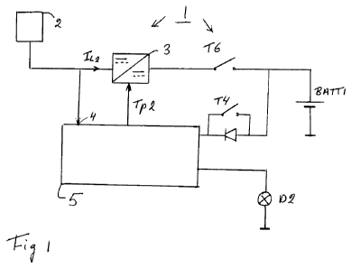
Fig. 1 shows a schematic block diagram of the power
conversion device including features of the present
invention;
Fig. 2 shows time graphs of pulse width and pulse
width period control according to the method of the present
invention; and
Fig. 3 shows a detailed schematic diagram of the
device of Fig. 1.
Fig. 1 shows a schematic block diagram and Fig. 2 shows the
diagram in further detail of a DC power converting device
CA 02682713 2009-09-30
WO 2008/120970 PCT/NL2007/050133
- 4 -
1, in particular a voltage up-converter, also called a
boost converter, comprising a DC source 2, such as a fuel
cell, a so called super capacitor or one or more solar
cells for loading one or more batteries BATT1 such as for
example a Ni-Cd, a Li-ion polymer or a Li polymer battery.
The device 1 further comprises a DC-DC converter, generally
indicated with reference numeral 3, which converter 3 is
coupled to the DC source 2. The converter 3 is provided
with an inductor L2, whose inductor current IL2 is
periodically controlled by a power controller 5 of the
device 1, which controller 5 is coupled to the converter 3
through control terminal TP2. The terminal TP2 is coupled
to the controller 5 through a so called totempole driver
comprising controllable semiconductors T3 and T4 which are
being controlled by a general purpose microprocessor IC1.
The controller 5 comprises a well known pulse width
modulator (not shown) for controlling the inductor current
IL2 during an adjustable block-sized part indicated TP2 in
upper Fig. 3 of consecutive pulse width periods P. In this
case the downward edge of the pulse is varied (indicated by
arrows) within the period P in accordance with a power
point tracking algorithm loaded in the controller 5. Such
an algorithm is equipped and fine tuned to optimise the
maximum power, rather than the maximum converter
efficiency, output by the device 1 as a whole to a load,
which is shown as one or two LED's D2 and D3. The LED's may
be on or off, or blink either or not in an alternating
fashion with some adjustable frequency. Here the LED's are
driven by the battery BATT1 which may at the same time be
loaded by the device 1 if a sufficient amount of solar
energy is provided to the solar cells 2, which together
with the batteries then form the actual DC source 2.
Fig. 3 shows the graphs necessary for understanding
the operation of the control of the PWM period P. During
the indicated block part TP2 in upper Fig. 3 the inductor
CA 02682713 2009-09-30
WO 2008/120970 PCT/NL2007/050133
- 5 -
current IL2 increases and due to the cutting of the current
at the downward edge of TP2 inductor coil L2 will provide
an induction voltage which through semiconductors D5 and T6
will provide a controlled levelled off battery current for
loading the battery. This process will repeat itself during
the subsequent periods P. P is normally of a fixed duration
and by varying in this mode the downward edge within period
P the loading optimally controlled by the mentioned
algorithm will keep track with the amount of light falling
on solar cell 2. The controller 5 comprises means
implemented in the microprocessor controller to adjust
during another mode the duration of the extended pulse
width period P', which is schematically shown in lower Fig.
3, where the duration of the new P' is approximately twice
that of the old P. This lowering of the PWM frequency
(1/P') leads to a reduction of the power consumption of the
controller 5. Adjusting means make the period P'
controllable and consequently influences the power
consumption of the controller, which applied in the device
1 saves power which would otherwise get lost during a
shorter duration of the PWM period P'. As in some countries
like ours sunlight is not as available as one would wish
for the purpose of effectively deriving sufficient solar
energy, the device 1 now makes it possible to apply solar
energy driven appliances on a broader scale, as even with
lower solar levels sufficiently mode controlled energy is
now becoming available for either charging the batteries 2
and/or for driving the loads D2, D3.
Of course switching of the controller 5 between an
active charging mode having shorter P' periods and a
reduced power consumption controller mode having longer P'
periods is possible. During the former mode the inductor
current magnitude IL2 is controlled through normal
adjustment of the part TP2 of the pulse width period and
during the latter mode the pulse width period P' is
CA 02682713 2009-09-30
WO 2008/120970 PCT/NL2007/050133
- 6 -
extended and now the pulse width part TP2' is adjusted.
If a solar cell appliances an important goal is to
withdraw maximum power from the solar cell under all
sunlight conditions. Based on knowledge of the solar cell a
percentage of for example approximately 80% of the open
terminal (no load) voltage of the solar cell is used by the
algorithm where above the controller 5 will be busy with
power point tracking for at least loading the battery
BATT1. If the open terminal voltage falls below said 80%
the solar cell current is low and then the controller 5 is
being switched from its converter mode to the low power
consuming (sleeping) mode during which the pulse width
period is extended, but during which the load (LED) current
is controlled. Advantageously this maximum power control
strategy needs no current measuring means and does not use
measured current for current control, which saves costs,
volume as well as valuable power. In practise the solar
current is however calculated, without being measured, and
used with some hysterese between switching points to
actually switch between the converter mode and the sleeping
mode.
During short moments in time the open terminal
voltage is periodically measured in order to effect a
temperature correction on the control strategy.
It is effective to apply a method and take the
necessary technical measures to derive the corresponding
pulse width frequency from a clock frequency provided by a
clock or local, possibly internal, generator generally
coupled through dividers, as such a generator or oscillator
is normally included in the micro-processor IC1 of the
power controller 5. As also a reduction of the clock
frequency reduces the power consumption of such a
controller that reduction now has a surplus effect as it
provides an extra power reduction, that is one due to the
lowering of the clock frequency and one due to the lowering
CA 02682713 2009-09-30
WO 2008/120970 PCT/NL2007/050133
- 7 -
of the PWM frequency.
Figs 1 and 2 show further features for saving
electric power. Semiconductor T6 which is also controlled
by the controller 5 under circumstances isolates source and
battery completely in order to prevent any leakage of
current through diode D5, which may be a Schottky diode
which is known to have a significant temperature dependent
leakage current, which would otherwise empty the battery.
Similarly semiconductor T4 which is controlled by the
controller 5 practically isolates the battery from the load
D2, D3 or acts as a semiconductor transition which lowers
the supply voltage VDD of the microprocessor controller 5
by one transition voltage (approx. 0.6 Volt) and thus
effectively reduces power consumption of the controller 5.
In that case T4 acts as a switchable controller supply
voltage reducing means for at least the controller 5.
Also the power consumed by the load D2, D3 may be
influenced and optimised by a controllable parallel
arrangement of resistors R6, and R11-R27, which are at the
one hand as a voltage divider coupled to the path between
the battery and the load and are at the other hand
connected to the power controller 5 for adequate inclusion
or exclusion of the resistors thereby. High ohmic resistors
R9 and R10 prevent IC1 outputs from unwantedly drawing
output currents.
The controller 5 comprises generally known decoding
means (not shown) coupled to the DC source 2 and pin 4 of
the controller 5 for enabling the controller if a
predetermined solar light sequence matches a sequence which
is stored in an internal memory of the controller 5. After
such enabling the controller 5 awakes from its sleep mode
to become active in controlling the inductor current IL2.
Pin 18 of the controller 5 is coupled to IR sensitive
semiconductor T5 for programming the controller 5 by means
of infrared radiation on T5.