Note: Descriptions are shown in the official language in which they were submitted.
CA 02683429 2016-05-25
VOLTAGE SURGE AND OVERVOLTAGE PROTECTION
BACKGROUND
[0001] Voltage surges created by lightning strikes and longer duration over-
voltages experienced on a power distribution grid can result in significant
damage to
electronic equipment. Where a sustained overvoltage is severe, fires have been
started resulting in significant loss of property. Existing surge protection
devices,
such as Transient Voltage Surge Suppressors (TVSS), are typically designed to
handle short duration transients of 8-20 microseconds associated with
lightning
strikes. As a result, TVSS devices typically provide no protection against
longer
duration over-voltage disturbances, and can often be the cause of the fires
and
damage to equipment that have been reported.
SUMMARY OF INVENTION
[0002] The following paragraphs describe various embodiments of the claimed
invention.
[0002a] In a preferred aspect, there is a system comprising: at least one
first
voltage clamping device (109) configured to clamp a voltage of an input AC
power
voltage (V) applied to an electrical load (103); at least one second voltage
clamping
device (113) configured to clamp the voltage of the input AC power applied to
the
electrical load (103); a switching element (R1) employed to selectively
establish a
direct coupling of the input AC power voltage (V) to the electrical load
(103); and a
processor circuit (143) that controls the operation of the switching element
(R1);
wherein the processor circuit (143) is designed and arranged to: store a
plurality of
predefined voltage-time thresholds (166) in a memory (406); monitor the input
AC
power voltage (V) to identify an overvoltage experienced in the input AC power
voltage (V) among the first clamping device (109) and the second clamping
device
(113); and time a duration of the overvoltage on the input AC power voltage by
controlling the switching element (R1) to selectively establish a coupling of
the input
AC power voltage (V) to the electrical load (103) such that, when the input AC
power
voltage (V) experiences an overvoltage that extends beyond one or more of the
voltage-time thresholds (166), the processor circuit (143) manipulates the
switching
element (R1) to at least partially isolate the electrical load (103) and the
second
1
CA 02683429 2016-05-25
[0002b] voltage clamping device (113) from the input AC power voltage (V)
until
the overvoltage has abated.
[0002c] In another aspect, there is a method comprising the steps of: applying
an
input AC power voltage (V) to an electrical load (103); distributing a
dissipation of an
overvoltage experienced in the input AC power voltage (V) among a first
clamping
device (109) and a second clamping device (113), the first and second clamping
devices (109, 113) being arranged in parallel; storing a plurality of
predefined
voltage-time thresholds (166) in a memory (406); monitoring the input AC power
voltage (V) to identify an overvoltage experienced in the input AC power
voltage (V)
among the first clamping device (109) and the second clamping device (113);
and
timing a duration of the overvoltage by controlling a switching element (R1)
to
selectively establish a coupling of the input AC power voltage (V) to the
electrical
load (103) such that, when the input AC power voltage (V) experiences an
overvoltage that extends beyond one or more of the voltage-time thresholds
(166), a
processor circuit (143) manipulates the switching element (R1) to at least
partially
isolate the electrical load (103) and the second voltage clamping device (113)
from
the input AC power voltage (V) until the overvoltage has abated.
[0002d] In yet another aspect, there is a voltage surge and overvoltage
protection
system comprising: at least one first voltage clamping device configured to
clamp a
voltage of an input power voltage applied to an electrical load to a
predetermined first
voltage clamping level; at least one second voltage clamping device configured
to
clamp the voltage applied to the electrical load to a predetermined second
voltage
clamping level; a series inductance coupled between the first and second
voltage
clamping devices; a selectably actuatable switch connected between the series
inductance and the second voltage clamping device for disconnecting power from
the
second voltage clamping device and the electrical load; and a switch control
circuit
that controls actuation of the switch in response to detection that the input
power
voltage has exceeded a predetermined voltage level for a predetermined time.
[0002e] In yet another aspect, there is a method to provide voltage surge and
overvoltage protection to an electrical load, comprising the steps of:
applying an input
power voltage to the electrical load; providing a first parallel clamping
device and a
second parallel clamping device between the input power voltage and the
electrical
load; distributing a dissipation of an overvoltage experienced in the input
power
voltage among the first parallel clamping device and the second parallel
clamping
device by separating the first and second parallel clamping devices with a
series
1a
CA 02683429 2016-05-25
inductance; monitoring the voltage of the input power voltage for an
overvoltage
having a magnitude and duration exceeding a predetermined voltage-time
threshold;
maintaining a direct coupling of the input power voltage to the electrical
load through
the first and second clamping devices so long as the magnitude and a duration
of the
overvoltage are less than said voltage-time threshold; and disconnecting the
direct
coupling of the input power voltage to the electrical load by opening a switch
connected between the series inductance and the second parallel clamping
device in
response to detection that the magnitude and duration of the overvoltage are
greater
than said voltage-time threshold.
[0002f] In yet another aspect, there is a system for conditioning an input
power
voltage applied to an electrical load, comprising: means for distributing a
dissipation
of an overvoltage experienced in the input power voltage among a first
parallel
clamping device and a second parallel clamping device; and means for
maintaining a
direct coupling of the input power voltage to the electrical load unless a
magnitude
and a duration of the overvoltage are less than at least one predefined
voltage-time
threshold; and means for disconnecting the direct coupling of the input power
voltage
by breaking the connection between the first parallel clamping device in
response to
detection that the magnitude and duration of the overvoltage are greater than
said at
least one predefined voltage-time threshold.
[0002g] In yet another aspect, there is an apparatus for protecting an
electrical
load from transient voltage surges and overvoltages when connected to an input
power voltage, comprising: at least one first voltage clamping device
connected to
the input power voltage configured to clamp the voltage of the input power
voltage to
a first predetermined clamping level; at least one second voltage clamping
device
connected to the electrical load configured to clamp the voltage applied to
the
electrical load to a second predetermined clamping level lower than said first
predetermined clamping level, in parallel arrangement with said first clamping
device;
a voltage detector circuit that provides a control signal representing the
input power
voltage; a processor circuit operative to provide a switching signal in
response to a
determination that the control signal from the voltage detector circuit
indicates that
the input power voltage exceeds a predetermined threshold for a predetermined
duration of time; a switch responsive to the switching signal from the
processor circuit
to switch between (i) a first state in which the input power voltage is
directly coupled
to the electrical load and first clamping device and (ii) a second state in
which the
direct coupling is opened and a shunt resistance is connected in parallel with
the load
1b
CA 02683429 2016-05-25
and the second clamping device; and a series inductance connected in between
the
first clamping device and the switch to distribute dissipation of overvoltage
across the
first and second voltage clamping devices when the switch is in the first
state.
[0002h] In yet another aspect, there is a voltage surge and overvoltage
protection
system, comprising: at least one first voltage clamping device configured to
clamp a
voltage of an input power voltage applied to an electrical load to a
predetermined first
voltage clamping level; at least one second voltage clamping device configured
to
clamp the voltage applied to the electrical load to a predetermined second
voltage
clamping level; a series inductance coupled between the first and second
voltage
clamping devices; a selectably actuatable switch connected between the series
inductance and the second voltage clamping device for disconnecting power from
the
second voltage clamping device and the electrical load; an high impedance
component coupled between the series inductance and the second voltage
clamping
device in parallel with the switch for providing isolation between the input
power
voltage to the electrical load when the switch is off; and a switch control
circuit that
controls actuation of the switch in response to detection that the input power
voltage
has exceeded a predetermined voltage level for a predetermined time
[0002i] In yet another aspect, there is a method for providing voltage surge
and
overvoltage protection to an electrical load, comprising the steps of:
applying an input
power voltage to the electrical load; providing a first parallel clamping
device and a
second parallel clamping device between the input power voltage and the
electrical
load; distributing a dissipation of an overvoltage experienced in the input
power
voltage among the first parallel clamping device and the second parallel
clamping
device by separating the first and second parallel clamping devices with a
series
inductance; providing a high impedance component between the series inductance
and the second parallel clamping device; monitoring the voltage of the input
power
voltage for an overvoltage having a magnitude and duration exceeding a
predetermined voltage-time threshold; maintaining a direct coupling of the
input
power voltage to the electrical load through the first and second clamping
devices so
long as the magnitude and a duration of the overvoltage are less than said
voltage-
time threshold; and disconnecting the direct coupling of the input power
voltage to
the electrical load by opening a switch connected between the series
inductance and
the second parallel clamping device in response to detection that the
magnitude and
duration of the overvoltage are greater than said voltage-time threshold and
coupling
1c
CA 02683429 2016-05-25
the high impedance component between the input power voltage and the
electrical
load.
[0002j] In yet another aspect, there is a system for conditioning an input
power
voltage applied to an electrical load, comprising: means for distributing a
dissipation
of an overvoltage experienced in the input power voltage among a first
parallel
clamping device and a second parallel clamping device; means for maintaining a
direct coupling of the input power voltage to the electrical load unless a
magnitude
and a duration of the overvoltage are less than at least one predefined
voltage-time
threshold; means for disconnecting the direct coupling of the input power
voltage by
breaking the connection between the first parallel clamping device in response
to
detection that the magnitude and duration of the overvoltage are greater than
said at
least one predefined voltage-time threshold; and means for providing a high
impedance between the first parallel clamping device and the second parallel
clamping device in response to the disconnecting of the direct coupling of the
input
power voltage to the electrical load by the disconnecting means.
[0002k] In yet another aspect, there is an apparatus for protecting an
electrical
load from transient voltage surges and overvoltages when connected to an input
power voltage, comprising: at least one first voltage clamping device
connected to
the input power voltage configured to clamp the voltage of level; at least one
second
voltage clamping device connected to the electrical load configured to clamp
the
voltage applied to the electrical load to a second predetermined clamping
level lower
than said first predetermined clamping level, in parallel arrangement with
said first
clamping device; a voltage detector circuit that provides a control signal
representing
the input power voltage; a processor circuit operative to provide a switching
signal in
response to a determination that the control signal from the voltage detector
circuit
indicates that the input power voltage exceeds a predetermined threshold for a
predetermined duration of time; a switch responsive to the switching signal
from the
processor circuit to switch between (i) a first state in which the input power
voltage is
directly coupled to the electrical load and first clamping device and (ii) a
second state
in which the direct coupling is opened and a high impedance component is
coupled
between the input power voltage and the electrical load prior to the second
clamping
device; and a series inductance connected in between the first clamping device
and
the switch to distribute dissipation of overvoltage across the first and
second voltage
clamping devices when the switch is in the first state.
id
CA 02683429 2016-05-25
[00021] In yet another aspect, there is a combination voltage surge,
overvoltage,
and inrush current protection system, comprising: at least one first voltage
clamping
device configured to clamp a voltage of an input power voltage applied to an
electrical load to a predetermined first voltage clamping level; at least one
second
voltage clamping device configured to clamp the voltage applied to the
electrical load
to a predetermined second voltage clamping level; a series inductance coupled
between the first and second voltage clamping devices; a current surge
detection
circuit for detecting the occurrence of a voltage sag condition on the input
power
voltage; a voltage detection circuit for detecting the occurrence of an
overvoltage
condition; an impedance component coupled between the inductance and the
electrical load; a selective actuatable switch coupled to the series
inductance for
disconnecting power from the electrical load and for reconnecting power to the
electrical load through the impedance component and via a direct coupling of
the
input power to the electrical load; and a switch control circuit that controls
the
operation of the switch, the switch control circuit responsive to detection of
a voltage
sag condition to connect the impedance between the input power voltage and the
electrical load to limit the inrush current upon termination of the voltage
sag condition
and responsive to an overvoltage condition to disconnect the input power
voltage
from the electrical load.
[0002m] In yet another aspect, there is a method for providing a combination
of
voltage surge, overvoltage, and inrush current protection to an electrical
load,
comprising the steps of: applying an input power voltage to an electrical
load;
distributing a dissipation of an overvoltage experienced in the power voltage
among a
first parallel clamping device and a second parallel clamping device by
separating the
first and second parallel clamping devices with a series inductance;
establishing a
direct coupling of the input power voltage to the electrical load unless a
magnitude
and a duration of the overvoltage are greater than at least one predefined
voltage-
time threshold; disconnecting the direct coupling of the input power voltage
to the
electrical load in response to detection of an overvoltage condition greater
than said
at least one predefined voltage-time threshold; and connecting the input power
voltage to the electrical load through an impedance component to reduce a
current
inrush in response to detection of a voltage sag condition.
[0002n] In yet another aspect, there is a method for providing a combination
of
overvoltage protection and inrush current protection to an electrical load,
comprising
the steps of: providing a disconnectable direct connection from an input power
le
CA 02683429 2016-05-25
voltage to the electrical load; detecting the voltage of an input power
voltage;
detecting the occurrence of a voltage sag condition in the input power voltage
that
can result in a potentially damaging current surge; in response to detecting
of a
voltage sag condition on the input power voltage, connecting an impedance
between
the input power voltage and the electrical load to limit inrush current upon
termination
of the voltage sag condition; and in response to detection of an overvoltage
condition, disconnecting the direct connection of the input power voltage to
the
electrical load.
[00020] In yet another aspect, there is a voltage surge and overvoltage
protection
system, comprising: at least one selectively disconnectable protection circuit
component for providing protection to an electrical load from an overvoltage
occurring on an input power voltage; a switching element employed to
selectively
disconnect the protection component; a memory for storing a plurality of
predefined
voltage-time curves corresponding to a plurality of predetermined voltage-time
thresholds; and a switch control circuit that controls the operation of the
switching
element to disconnect the protection circuit component from the input power
voltage
in response to detection that a duration and magnitude of the input power
voltage
exceeds one of the predetermined voltage-time thresholds represented by one of
the
plurality of voltage-time curves stored in the memory.
[0002p] In yet another aspect, there is a method for providing voltage surge
and
overvoltage protection to an electrical load, comprising the steps of:
applying an input
power voltage to the electrical load; providing at least one selectively
disconnectable
protection circuit component for providing protection to the electrical load
from an
overvoltage occurring on the input power voltage; storing a plurality of
predefined
voltage-time curves corresponding to a plurality of predetermined voltage-time
thresholds in a memory; detecting a magnitude and duration of the input power
voltage; and disconnecting the protection circuit component from the input
power
voltage in response to detection that the magnitude and a duration of an
overvoltage
are greater than at least one predefined voltage-time thresholds stored in the
memory.
[0002q] In yet another aspect, there is a system, comprising: at least one
first
voltage clamping device configured to clamp a voltage of an input power
voltage
applied to an electrical load; at least one second voltage clamping device
configured
to clamp the voltage applied to the electrical load; an inductance arranged
between
the first and second voltage clamping devices; a switching element employed to
if
CA 02683429 2016-05-25
selectively establish a coupling of the input power voltage to the electrical
load; and a
processor circuit that controls the operation of the switching element, the
processor
circuit operative to: store a plurality of predefined voltage-time thresholds
in a
memory; monitor the input power voltage to identify an overvoltage experienced
in
the power voltage among the first clamping device and the second clamping
device;
and time a duration of the overvoltage by controlling the switching element to
selectively establish a coupling of the input power voltage to the electrical
load such
that, when the input power voltage experiences an overvoltage that extends
beyond
one or more of the voltage-time thresholds, the processor circuit manipulates
the
switching element to at least partially isolate the electrical load and the
second
voltage clamping device from the power voltage until the overvoltage has
abated.
[0002r] In yet another aspect, there is a method, comprising the steps of:
applying
an input power voltage to an electrical load; distributing a dissipation of an
overvoltage experienced in the input power voltage among a first clamping
device
and a second clamping device by arranging an inductance between the first and
second clamping devices, the first and second clamping devices being arranged
in
parallel; storing a plurality of predefined voltage-time thresholds in a
memory;
monitoring the input power voltage to identify an overvoltage experienced in
the input
power voltage among the first clamping device and the second clamping device;
and
timing a duration of the overvoltage by controlling a switching element to
selectively
establish a coupling of the input power voltage to the electrical load such
that, when
the input power voltage experiences an overvoltage that extends beyond one or
more of the voltage-time thresholds, a processor circuit manipulates the
switching
element to at least partially isolate the electrical load and the second
voltage
clamping device from the input power voltage until the overvoltage has abated.
[0002s] In yet another aspect, there is a voltage surge and overvoltage
protection
system, comprising: at least one first voltage clamping device configured to
clamp a
voltage of an input power voltage applied to an electrical load to a
predetermined first
voltage clamping level; at least one second voltage clamping device configured
to
clamp the voltage applied to the electrical load to a predetermined second
voltage
clamping level; a selectably actuatable switch connected between the first
voltage
clamping device and the second voltage clamping device for disconnecting power
from the second voltage clamping device and the electrical load; and a switch
control
circuit that controls actuation of the switch in response to detection that
the input
power voltage has exceeded a predetermined voltage level for a predetermined
time.
1g
CA 02683429 2016-05-25
[0002t] In yet another aspect, there is a method for providing voltage surge
and
overvoltage protection to an electrical load, comprising the steps of:
applying an input
power voltage to the electrical load; providing a first parallel clamping
device and a
second parallel clamping device between the input power voltage and the
electrical
load; distributing a dissipation of an overvoltage experienced in the input
power
voltage among the first parallel clamping device and the second parallel
clamping
device; monitoring the voltage of the input power voltage for an overvoltage
having a
magnitude and duration exceeding a predetermined voltage-time threshold;
maintaining a direct coupling of the input power voltage to the electrical
load through
the first and second clamping devices so long as the magnitude and a duration
of the
overvoltage are less than said voltage-time threshold; and disconnecting the
direct
coupling of the input power voltage to the electrical load by opening a switch
connected between the first parallel clamping device and the second parallel
clamping device in response to detection that the magnitude and duration of
the
overvoltage are greater than said voltage-time threshold.
BRIEF DESCRIPTION OF THE DRAWINGS
[0003] Many aspects of the present disclosure can be better understood with
reference to the following drawings. The components in the drawings are not
necessarily to scale, emphasis instead being placed upon clearly illustrating
the
principles of the disclosure. Moreover, in the drawings, like reference
numerals
designate corresponding parts throughout the several views.
[0004] FIG. 1 is a schematic of one example of a voltage surge suppressor
according to various embodiments of the present disclosure;
[0005] FIG. 2 is a graph depicting examples of voltage-time curves employed in
the operation of the voltage surge suppressors of FIG. 1 according to various
embodiments of the present disclosure;
[0006] FIG. 3 is a state diagram that provides one example of the operation of
the voltage surge suppressor of FIG. 1 according to various embodiments of the
present disclosure;
1h
CA 02683429 2009-10-02
WO 2008/124587
PCT/US2008/059406
[0007] FIG. 4 is a flow chart illustrating one example of a power up routine
of
the voltage surge suppressor of FIG. 1 according to various embodiments of the
present disclosure;
[0008] FIGS. 5A and 5B are flow charts illustrating one example of a response
of the voltage surge suppressor of FIG. 1 to a voltage sag according to
various
embodiments of the present disclosure;
[0009] FIG. 6 is a flow chart that illustrates one example of a response of
the
voltage surge suppressor of FIG. 1 to a moderate overvoltage according to
various
embodiments of the present disclosure;
[0010] FIG. 7 is a flow chart that illustrates an example of a response of the
voltage surge suppressor of FIG. 1 to a severe overvoltage according to
various
embodiments of the present disclosure;
[0011] FIG. 8 is a schematic of another example of a second transient voltage
surge suppressor according to various embodiments of the present disclosure;
[0012] FIG. 9 is a state diagram that provides one example of the operation of
the transient voltage surge suppressor of FIG. 8 according to various
embodiments
of the present disclosure;
[0013] FIG. 10 is a flow chart illustrating one example of a power up routine
of
the transient voltage surge suppressor of FIG. 8 according to various
embodiments
of the present disclosure;
[0014] FIG. 11 is a flow chart that illustrates one example of a response of
the
transient voltage surge suppressor of FIG. 8 to an overvoltage or voltage sag
according to various embodiments of the present disclosure;
[0015] FIG. 12 is a flow chart that illustrates one example of a routine that
restores the transient voltage surge suppressor of FIG. 8 to a nominal state
after an
overvoltage or voltage sag in the power voltage has ended according to various
embodiments of the present disclosure;
[0016] FIG. 13 is a schematic block diagram of a processor circuit employed in
the voltage surge suppressors of FIGS. 1 or 8 according to various embodiments
of
the present disclosure;
[0017] FIG. 14 depicts one example of a plot of a line voltage with respect to
time that illustrates the timing relating to the insertion and removal of a
current
2
CA 02683429 2009-10-02
WO 2008/124587
PCT/US2008/059406
limiting impedance in association with the voltage sag according to an
embodiment
of the present disclosure;
[0018] FIG. 15 is a schematic of one example of a current limiting circuit
that
operates to time the removal of a current limiting impedance as illustrated,
for
example, in FIG. 14 according to an embodiment of the present disclosure;
[0019] FIG. 15 is a schematic of another example of a current limiting circuit
that
operates to time the removal of a current limiting impedance as illustrated,
for
example, in FIG. 14 according to an embodiment of the present disclosure;
[0020] FIG. 17 is a schematic of yet another example of a current limiting
circuit
that operates to time the removal of a current limiting impedance as
illustrated, for
example, in FIG. 14 according to an embodiment of the present disclosure;
[0021] FIG. 18 is a graph that plots one example of an inrush surge current
with
respect to a duration of a sag in a power voltage such as the voltage sag
illustrated
in the example depicted in FIG. 14, where the inrush surge current depicted
provides one example basis for determining where the current limiting
impedance
depicted with respect to FIGS. 15, 16, or 17 should be removed according to an
embodiment of the present disclosure;
[0022] FIG. 19 is a schematic diagram of one example of a processor circuit
that executes gate drive logic as employed in the current limiting circuits of
FIGS.
15, 16, or 17 according to an embodiment of the present disclosure; and
[0023] FIG. 20 is a flow chart of one example of the gate drive logic executed
in
the processor of FIG. 18 according to an embodiment of the present disclosure.
DETAILED DESCRIPTION
[0024] With reference to FIG. 1, shown is one example of a voltage protector
100 according to various embodiments of the present disclosure. The voltage
protector 100 includes an input terminal through which an input power voltage
V is
received. The power voltage V comprises a nominal voltage that is a standard
value, specified for various purposes such as power distribution on a power
grid, i.e.
120/240 single phase, 480/277 Wye, 120/208 Wye or other specification. Nominal
voltages may be generated at various frequencies such as 60 Hz., 50 Hz., 400
Hz.,
or any other frequency. Thus, a nominal voltage may be an AC voltages
specified,
for example, in terms of peak to peak voltage, RMS voltage, and/or frequency.
3
CA 02683429 2009-10-02
WO 2008/124587
PCT/US2008/059406
Also, a nominal voltage may be a DC voltage specified in terms of a voltage
magnitude.
[0025] From time to time, the power voltage V may experience an overvoltage
that may last many milliseconds or even longer. Such overvoltages may be
caused
by a variety of incidents, including faults in the power distribution system
or the
switching of capacitors into and out of the power distribution grid for
purposes of
voltage regulation. Also, in split 240 volt single phase systems, for example,
the
loss of the neutral conductor due to a fault, cut conductor, or other problem
can
result in overvoltages. Still further, the power voltage V may experience
voltage
sags from time to time, resulting in potentially harmful inrush current into
sensitive
electronic equipment at the end of the voltage sag event.
[0026] The voltage protector 100 includes phase, neutral, and ground
conductors that are used to route the power voltage V to an electrical load
103 that
is coupled to the transient voltage surge suppressor 100. In this respect, the
voltage protector 100 may be embodied in a power strip, a load center, or
other
location.
[0027] The voltage protector 100 includes a thermal fuse 106 that operates as
a
safety circuit interrupt as can be appreciated. The voltage protector 100 also
includes first voltage clamping device 109 and a second voltage clamping
device
113. As will be discussed further below, the voltage clamping level of the
first
voltage clamping device 109 is substantially higher than the voltage clamping
level
of the second voltage clamping device 113. The first voltage clamping device
109
is coupled from phase cp to neutral N at the power input of the voltage
protector 100.
The second voltage clamping device 113 is coupled from phase cp to neutral N
at
the power output of the voltage protector 100 in parallel with the electrical
load 103
when coupled thereto.
[0028] The voltage protector 100 further comprises a series inductance L, a
first
switching element R1 and a second switching element R2. The series inductance
L
is positioned in the phase conductor between the first and second clamping
devices
109 and 113. The first and second switching elements R1 and R2 are coupled in
parallel to each other as shown. The first switching element R1 includes a
first
state and a second state. In the first state, the first switching element R1
couples
the series inductance L directly to the electrical load 103. In a second
state, the first
4
CA 02683429 2009-10-02
WO 2008/124587
PCT/US2008/059406
switching element R1 couples a shunt resistance Rs across the phase cp and
neutral
N conductors in parallel with the load 103. Where the electrical load 103 is
inductive, the shunt resistance RS allows the inductive load to discharge and
provides a pathway for leakage currents as can be appreciated.
[0029] The second switch element R2 includes a first state and a second state.
In the first state, the second switch element R2 couples an impedance between
the
series inductance L and the electrical load 103. In this sense, the second
switch
element R2 adds an impedance to the electrical load 103. In a second state,
the
second switch element R2 is open. The first and second switching elements R1
and R2 may comprise, for example, relays, solid state switches such as
thyristors,
or other types of switching circuit elements.
[0030] Coupled to the second switching element R2 is an impedance 126 that
comprises, for example, a negative temperature coefficient resistor
(thermistor) or
other impedance. In addition, the voltage protector 100 includes a voltage
clamping
device 133 coupled between phase cp and ground G, and a voltage clamping
device
136 coupled between neutral N and ground G. The voltage clamping devices 109,
113, 133, and 136 may comprise, for example, metal oxide varistors, zener
diodes,
gas tubes, or other voltage clamping circuit elements.
[0031] Still further, the voltage protector 100 includes a processor circuit
143
that controls the operation of the first and second switching elements R1 and
R2.
The voltage protector 100 also includes a current surge detection interface
circuit
146, a voltage detection interface circuit 149, and a power circuit 153. The
current
surge detection interface circuit 146, the voltage detection interface circuit
149, and
the power circuit 153 each receive an input voltage taken across the phase cp
and
neutral N conductors between the inductance L and the first and second
switches
R2.
[0032] The current surge detection interface circuit 146 detects whether a
voltage sag exists that can result in a potentially damaging current surge.
[0033] The voltage detection interface circuit 149 detects the power voltage V
and provides an appropriate signal to the processor circuit 143. By knowing
the
voltage at any given moment, the processor circuit 143 can take such action as
is
deemed necessary to protect components of the voltage protector 100 and the
electrical load 103 from voltage surge and voltage sag activity as will be
described.
CA 02683429 2009-10-02
WO 2008/124587
PCT/US2008/059406
The current surge detection interface circuit 146 and the voltage detection
interface
circuit 149 are designed to provide a fast response to overvoltage and voltage
sag
conditions. The microprocessor is selected so as to provide for fast switching
of the
switching elements R1 and R2.
[0034] The power circuit 153 generates DC power that is applied to the
processor circuit 143 to power its operation as can be appreciated.
[0035] Referring next to FIG. 2, shown is a voltage-time chart 163 that
depicts
several voltage-time curves 166 that act as predefined voltage-time thresholds
that
are used by the processor circuit 143 to control the operation of the first
and second
switching elements R1 and R2 (FIG. 1). The data associated with the voltage-
time
curves 166 is stored in a memory associated with the processor circuit 143.
[0036] Each curve 166 represents a magnitude-duration threshold for an
overvoltage in the power voltage V (FIG. 1) that is used to determine when the
processor circuit 143 is to take action to prevent potential electrical damage
to
circuitry due to an overvoltage. This is to say, if a magnitude of an
overvoltage lasts
long enough, the amount of energy inherent in the overvoltage may cause damage
to circuitry as will be discussed. The voltage-time curves 166 act as
magnitude-
duration thresholds by which it may be determined that there is too much
energy in
an overvoltage to be handled by the first and second voltage clamping devices
109
and 113.
[0037] In this respect, for example, assume that the power voltage V applied
to
the voltage protector 100 (FIG. 1) has a nominal value of 120 volts RMS at 60
Hz.
According to one embodiment, any overvoltage experienced by the power voltage
V
that is less than 15% over the nominal 120 volt RMS value is a "safe" value
such
that the voltage protector 100 continues to supply the power voltage V to the
load
103 through the series inductance L. However, if the power voltage V is equal
to or
greater than the 115% of the nominal voltage for a predefined period of time,
for
example, then the voltage protector 100 may take action to protect the voltage
clamping devices 109 and 113, and the electrical load 103 from the
overvoltage. In
this respect, the voltage clamping devices 109 and 113 may conduct current due
to
the overvoltage, but may become overheated or may experience other damage
causing a fire hazard if the overvoltage moves beyond the specified voltage-
time
curves 166.
6
CA 02683429 2009-10-02
WO 2008/124587
PCT/US2008/059406
[0038] During operation of the voltage protector 100, the first and second
voltage clamping devices 109 and 113 operate to dissipate voltage transients
and
overvoltages to protect the electrical load 103. Specifically, when a high
voltage
transient such as caused by a lightning strike is experienced in the power
voltage V,
it first encounters the first voltage clamping device 109 that begins to
conduct. The
series inductance slows down the propagation of the voltage transient or
overvoltage to allow the first voltage clamping device 109 to clamp the
voltage at its
clamping level. The second voltage clamping device 113 then conducts any
excess
voltage to ground G that passes through the series inductance L. According to
one
embodiment, since the clamping level (i.e. 300 volts) of the second voltage
clamping device 113 is approximately one half the clamping level (i.e. 600
volts) of
the first voltage clamping device 109, then the dissipation of the excess
voltage
experienced from a voltage transient or overvoltage is distributed between the
first
and second voltage clamping devices 109 and 113.
[0039] As mentioned above, the voltage clamping level of the first voltage
clamping device 109 may comprise, for example, 600 volts, and the second
voltage
clamping device 113 may have a clamping level of 300 volts as can be
appreciated.
Alternatively, some other ratio of clamping voltages may exist between the
first and
second voltage clamping devices 109 and 113. The specific voltage clamping
levels of the first and second voltage clamping devices 109 and 113 also
depend
upon the nominal value of the power voltage V. It should be noted that even
though
the clamping voltage of the first clamping device 109 is 600 volts, the
electrical load
103 is never exposed to a voltage that is higher than the clamping voltage of
the
second clamping device 113 (i.e. 300 volts). Also, the first voltage clamping
device
109 affords protection against voltage transients and the like even if the
switching
elements R1 and R2 are in an off state.
[0040] The processor circuit 143 is configured to control the first and second
switching elements R1 and R2 to selectively establish a direct coupling of the
power
voltage V to the electrical load 103. In this respect, when the power voltage
V
experiences an overvoltage that extends beyond one or more of the voltage-time
curves 166, the processor circuit is configured to manipulate the switching
elements
R1 and R2 in order to at least partially isolate the electrical load 103 and
the second
voltage clamping device 113 from the power voltage V until the overvoltage has
7
CA 02683429 2009-10-02
WO 2008/124587
PCT/US2008/059406
abated. In one embodiment, the electrical load 103 is entirely decoupled from
the
power voltage V where the switching elements R1 and R2 are in the off state as
will
be described.
[0041] In this respect, the second voltage clamping device 113 with a lower
conduction voltage dissipates the bulk of the energy in the case of sustained
overvoltage from incoming line to neutral N. Where the dissipation due to the
overvoltage is so great that the first or second voltage clamping device 109
or 113
may overheat or burn up, the thermal fuse 106 will blow, thereby protecting
all of
the circuitry in the voltage protector 100. Other implementations for
protecting the
voltage clamping devices with thermal fuses are well known and will not be
discussed in greater detail herein.
[0042] Thus, the voltage protector 100 advantageously ensures that the
electrical load 103 is protected from voltage transients and overvoltages
without
presenting a fire hazard. Where the voltage clamping devices 109 and 113
comprise metal oxide varistors, they may only last 8 to 10 milliseconds under
typically encountered overvoltage conditions while dissipating significant
energy
before overheating or damage results. To this end, the design of the voltage
protectors as described herein take into account the limited capabilities of
such
voltage clamping devices.
[0043] Typical transient voltage surge suppressors do not take such
limitations
into account. For example, even in the rare case where over-voltage protection
is
claimed, metal oxide varistors used may be subject to over-voltages for as
much as
100-200 milliseconds, which is enough to permanently damage the metal oxide
varistors.
[0044] Note that the voltage-time curves 166 are specified so as to prevent
the
processor circuit from implementing nuisance switching of the switching
elements
109 and 113 to isolate the electrical load 103 during overvoltages that may
not be
high enough to cause damage. In this respect, some degree of overvoltage is
tolerated in order to prevent unwarranted disruption of the operation of the
electrical
load 103. Such overvoltages are those that do not result in the overheating of
the
first and second voltage clamping devices 109 and 113, or cause damage to the
electrical load 103.
8
CA 02683429 2009-10-02
WO 2008/124587
PCT/US2008/059406
[0045] In view of the foregoing, the operation of the voltage protector 100 is
discussed with greater particularity with reference to the figures that
follow.
[0046] With reference to FIG. 3, shown is a state diagram 173 that depicts the
operation of logic executed within the processor circuit 143 according to an
embodiment. Alternatively, the state diagram 173 of FIG. 3 may be viewed as
depicting steps of a method implemented in the processor circuit 143.
[0047] The state diagram 173 includes a "power off" state 176, a "nominal"
state
179, a "voltage sag" state 183, and an "isolation" state 186. The "power off'
state
176 is the state of the processor circuit 143 when there is no power is
applied to the
inputs of the processor circuit 143. Assuming that power is applied to the
voltage
protector 100, then a power up routine 189 is implemented to transition the
state of
the processor circuit 143 from the power off state 176 to the nominal state
179. The
nominal state 179 represents a normal operating state of the processor circuit
143
such that the power voltage V is nominal and no voltage anomalies such as
transients or overvoltages are experienced as described above. If power is
lost
while the processor circuit 143 is in the nominal state 179, the voltage sag
state
183, or the isolation state 186, then the processor circuit 143 reverts to the
power
off state 176.
[0048] If, while in the nominal state 179, a voltage sag occurs in the power
voltage V, then a "voltage sag" routine 193 is implemented so as to transition
the
operation of the processor circuit 143 to the voltage sag state 183. In the
voltage
sag state, the processor circuit 143 waits until a voltage sag has come to an
end in
order to transition back to the nominal state 179. In transitioning back to
the
nominal state, the processor circuit 143 will implement a "voltage sag over"
routine
196.
[0049] In addition, if while in the nominal state 179, the voltage protector
100
experiences an overvoltage, the processor circuit 143 will decide whether it
is
necessary to enter the isolation state 186 depending upon whether the
overvoltage
exceeds a given one of the voltage-time curves 166 as described above. In some
cases, overvoltages may comprise moderate overvoltages that may not provide
immediate harm to the electrical load 103. However, if the duration of such
moderate overvoltages lasts beyond the time specified by a given one of the
voltage-time curves 166, then such moderate overvoltage may become damaging
9
CA 02683429 2009-10-02
WO 2008/124587
PCT/US2008/059406
due to the excess energy involved. In such case, the processor circuit 143
transitions to the isolation state 186 by implementing a "moderate
overvoltage"
routine 199. However, if a severe overvoltage occurs such that imminent damage
to the electrical load 103 and the voltage clamping devices 109 and 113 may
occur,
then the processor circuit 143 will transition from the nominal state 179 to
the
isolation state 186 by implementing a "severe overvoltage" routine 203.
[0050] When in the isolation state 186, a direct coupling between the input
power voltage V and the load 103 is disconnected such that the electrical load
103
is at least partially isolated from the power voltage V during the duration of
the
potentially damaging overvoltage. When the moderate or severe overvoltage is
over and the power voltage V has returned to nominal while in the isolation
state
186, then the processor circuit 143 returns to the nominal state 179 by
implementing a "restore power" routine 206. Examples of the various routines
described above in transitioning between the respective operational states
will be
provided in the discussion that follows. It is understood that each flow chart
depicted may be viewed as depicting the operation of the processor circuit
143, or
such flow charts may be viewed as depicting steps of methods implemented in
the
voltage protector 100. In one embodiment, the flow charts depict functionality
that
may be implemented with any one of a number of programming languages
associated with processor circuits that may be employed.
[0051] Referring next to FIG. 4, shown is one example of the power up routine
189 that occurs upon initial power up of the processor circuit 143 when the
voltage
protector 100 is first placed into an operational state with respect to an
electrical
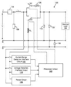
load 103 as can be appreciated. Once the power voltage V is first applied to
the
input terminals of the voltage protector 100, in box 223, the processor
circuit 143 is
initialized as can be appreciated. In this initial state, the relays R1 and R2
are in the
off positions (the first state) such that R1 couples the load through the
resistor Rs to
neutral N and R2 presents an open circuit.
[0052] By virtue of the fact that the switching elements R1 and R2 are off
when
power is first applied, the electrical load 103 is isolated from the power
voltage V.
This is advantageous due to the fact that the power voltage V may be
experiencing
an overvoltage while the processor circuit 143 is first initializing.
Specifically,
because the processor circuit 143 is initializing when first powered up, it is
not in a
CA 02683429 2009-10-02
WO 2008/124587
PCT/US2008/059406
position to operate the switching elements R1 and R2 in order to adequately
protect
the electrical load 103. Accordingly, the switching elements R1 and R2 are
specified to be in an off state upon the startup of the voltage protector 100
so as to
protect the electrical load 103 during the initialization phase.
[0053] Next, in box 226, the initialization process proceeds until it has
completed. Assuming that the processor circuit 143 is initialized, then box
227 the
processor circuit 143 determines whether the power voltage V is currently
experiencing an overvoltage such as a moderate or severe overvoltage. If no
overvoltage is currently being experienced, then the processor circuit 143
proceeds
to box 229. On the other hand, if an overvoltage exists, then the processor
circuit
143 proceeds to box 228 in which the processor circuit 143 waits until the
voltage
has returned to nominal. Thereafter, the processor circuit 143 proceeds to box
229
as shown.
[0054] In box 229 the processor circuit 143 causes the switching element R2 to
turn on in order to place the thermistor 126 into the circuit to limit an
inrush current
into the electrical load 103 during the initial power up of the load 103. In
box 233,
the processor circuit 143 initiates a timer. This timer effectively determines
a period
of time for the electrical load 103 to fully power up with the thermistor 126
in the
circuit, thereby ensuring that there will be no damaging inrush current to the
electrical load 103.
[0055] In box 236, the processor circuit 143 determines whether the timer has
reached a predefined time within which any potential inrush current into the
electrical load 103 will have been abated. Assuming that the timer has reached
the
predefined time in box 236, then in box 239, the processor circuit 143 turns
on
switching element R1, thereby directly coupling the power voltage V to the
electrical
load 103 and bypassing the thermistor 126. In this respect, the thermistor 126
is
bypassed as the direct coupling presented through the switching element R1
provides the path of least resistance to the electrical load 103.
[0056] Then, in box 243, the switching element R2 is turned off, thereby
opening the circuit. Note that due to the fact that the switching element R2
is
closed when switching element R1 was turned on, the voltage seen across
switching element R1 at such time will be the voltage across the thermistor
126.
This voltage is relatively low given that the thermistor 126 is added in
series with the
11
CA 02683429 2009-10-02
WO 2008/124587
PCT/US2008/059406
load 103. Where the switching element R1 is a relay, this fact advantageously
prevents a significant voltage from developing over the contacts of a relay
R1,
thereby preventing significant sparking during the switching of the relay R1.
Such
sparking might otherwise result in damage to the relay over time that will
significantly degrade its performance and lifespan. Thereafter, the processor
circuit
143 enters nominal state 179.
[0057] With reference to FIG. 5A, shown is one example of the voltage sag
routine 193 that is implemented in order to transition from the nominal state
179 to
the voltage sag state 183. The voltage sag routine 193 is implemented when the
processor circuit 143 detects a voltage sag in the power voltage V as
described
above. The actually magnitude and duration of a voltage sag that causes the
implementation of the voltage sag routine 193 can be predetermined. In one
embodiment, the magnitude and duration of such a voltage sag may be specified
such that voltage sags that are more severe than the predetermined threshold
would result in a significant inrush current into the electrical load 103 when
the
power voltage V returns to nominal. However, the threshold voltage sag should
be
defined so as to prevent nuisance switching, etc. In one embodiment, a voltage
sag
of less than 75% nominal voltage for more than 2 to 3 cycles might result in
significant current inrush. In another example, a voltage sage of 85% nominal
voltage or higher for a few cycles would be ignored as a potential nuisance
switching event.
[0058] The voltage sag routine 193 begins with box 253 in which the switching
element R2 is turned on, thereby inserting the thermistor 126 into the
circuit. At
some point after R2 is turned on, in box 256, the switching element R1 is
turned off.
This causes the power voltage to be supplied to the electrical load 123
through the
thermistor 126. Assuming that the switching element R1 is a relay, then by
turning
the switching element R2 on before turning the switching element R1 off, the
voltage across the contacts of the relay R1 is equal to the voltage across the
thermistor 126, thereby minimizing sparking across the contacts of the relay
that
can degrade the performance and lifespan of the relay as described above.
[0059] Thereafter, the voltage sag routine 193 ends and the processor circuit
143 is placed in the voltage sag state 183 in which the processor circuits
waits until
the voltage sag ends and the power voltage V returns to nominal. The level of
12
CA 02683429 2009-10-02
WO 2008/124587
PCT/US2008/059406
voltage of the power voltage that qualifies as the voltage sag that would
cause the
implementation of the voltage sag routine 193 may be predetermined as can be
appreciated.
[0060] With reference then to FIG. 5B, shown is one example of the "voltage
sag over" routine 196 that is employed when transitioning from the voltage sag
state
183 back to the nominal state 179. The voltage sag over routine 196 is
implemented when the processor circuit 143 detects that the power voltage V
has
returned to a nominal state based upon inputs from the voltage detect
interface
circuit 149 (FIG. 1).
[0061] When in the voltage sag state 183, the switching element R2 is in an
off
state, where power is supplied to the electrical load 103 through the
thermistor 126.
Also, the switching element R1 is in an off position such that the electrical
load 103
is in parallel with the shunt resistance Rs.
[0062] To begin, in box 263, the voltage sag over routine 196 turns on R1 at
an
optimal point in the power voltage cycle. The optimal point in the power cycle
is
one that minimizes the creation of an inrush current in the electrical load
103. In
particular, reference is made to the discussion of FIGS. 14-20 that mention
the
timing at which a thyristor or relay is controlled to establish the
application of power
voltage to the electrical load 103 while minimizing an inrush current to the
electrical
load 103. Once the switching element R1 is turned on at the optimal point in
box
263, then the switching element R2 is turned off to allow the steady state
operation
of the load 103.
[0063] Referring next to FIG. 6, shown is a flowchart that provides one
example
of the moderate overvoltage routine 199 that is executed, for example, to
transition
the operation of the processor circuit 143 from the nominal state 179 to the
isolation
state 186 according to various embodiments. To begin, a moderate overvoltage
199 is detected when an overvoltage experienced in the power voltage V is such
that it is greater than the minimum voltage-time curve 166, but is less than a
voltage-time curve 166 that would deem to be immediately damaging to the
electrical load 103 (i.e. a severe overvoltage). As such, moderate
overvoltages
may exist according for a predefined period of time before they are considered
damaging. When the moderate overvoltage reaches the point where it may be
potentially damaging, action may be taken to protect the various components of
the
13
CA 02683429 2009-10-02
WO 2008/124587
PCT/US2008/059406
voltage protector 100 and the electrical load 103 in a manner that minimizes
potential damage to switching elements R1 as will be described.
[0064] Beginning with box 273, the moderate overvoltage routine 199 initiates
a
timer 273. This timer is initiated in order to measure the duration of the
overvoltage
so that it can be compared with a given voltage-time curve 166 stored in the
memory associated with the processor circuit 143. In box 273, it is determined
whether to decouple the electrical load 103 from the power voltage V based
upon
whether the moderate overvoltage is greater than one of the given voltage-time
curves 166 stored in the memory of the processor circuit 143.
[0065] Assuming that the electrical load 103 is to be decoupled from the power
voltage V, then in box 279, the relay R2 is turned on, thereby injecting the
thermistor 126 in series with the electrical load 103. Thereafter, in box 283,
a delay
is imposed upon the operation of the moderate overvoltage routine 199. Then,
in
box 286, the switching element R1 is switched off, thereby coupling the shunt
resistance Rs across faced neutral in parallel with the electrical load 103.
[0066] In this situation, the power voltage V is applied to the electrical
load 103
through the thermistor 126. This is advantageous as the voltage across the
thermistor 126 is a relatively low voltage, which means that the voltage
across the
switching element R1 is equal to such voltage since the switching element R1
is in
parallel with the switching element R2 and the thermistor 126. If the
switching
element R1 comprises a relay, then this lower voltage will minimize any
sparking
experienced at the contacts of the relay when turned off, thereby preventing
major
damage to the relay as described above.
[0067] In box 289, a further delay is imposed upon the implementation of the
moderate overvoltage routine 199. Then in box 291, the switching element R2 is
turned off, thereby completely decoupling the electrical load 103 from the
power
voltage V. Thereafter, the voltage protector 100 enters the isolation state
186 in
which the electrical load 103 is isolated from the power voltage V until the
overvoltage has ended and the power voltage V has returned to nominal. This
action prevents the electrical load 103 from experiencing a potentially
damaging
overvoltage. Also, the first and second voltage clamping devices 109 and 113
are
prevented from overheating and/or causing a fire, etc. At the same time, where
the
switching element R1 is a relay, the lifespan of the relay is extended.
14
CA 02683429 2009-10-02
WO 2008/124587
PCT/US2008/059406
[0068] Referring next to FIG. 7, shown is a flowchart that provides one
example
of the operation of the severe overvoltage routine 203 according to various
embodiments. The severe overvoltage routine 203 transitions the processor
circuit
143 from the nominal state 179 to the isolation state 186 in response to a
severe
overvoltage experienced in the power voltage V. A severe overvoltage is
considered to be an overvoltage that is so high that immediate damage is
threatened to the electrical load 103 and/or the first and second voltage
clamping
devices 109 and 113. In this respect, a severe overvoltage may result in
physical
damage to the second voltage clamping device 113 that may render it
inoperative
and potentially cause a fire or other malfunction.
[0069] A severe overvoltage may be defined by a predefined voltage-time curve
166 stored in a memory associated with the processor circuit 143. Beginning
with
box 293, the severe overvoltage routine 203 starts a timer. Then in box 296,
the
severe overvoltage routine 203 determines whether a severe overvoltage has
occurred for a required predefined period of time, thereby necessitating
isolation of
the electrical load 103 from the power voltage V in an attempt to prevent
destruction
of the second voltage clamping device 113, and to protect the electrical load
103.
Assuming that the duration of the severe overvoltage has reached the
prescribed
time specified in a respective voltage-time curve 166 associated with a severe
overvoltage, then in box 299, the switching element R1 is turned off.
[0070] It may be the case where the switching element R1 comprises a relay
that a significant spark may occur across the contacts of the relay R1 when it
is
turned off in this context since the switching element R2 is turned off at the
same
time. However, due to the potential damaging nature of the severe overvoltage,
the
damage that potentially may occur to the relay in this context is tolerated,
even if
such damage might result in undue degradation of the relay R1 and shorten its
lifespan. However, given that the occurrences of such severe overvoltages are
relatively rare, the potential damage in this context is tolerated rather than
allowing
the first and second voltage clamping devices 109 and 113 to be overheated or
cause a fire, as well as to prevent damage to the electrical load 103.
Thereafter,
the processor circuit 143 enters the isolation state 196 in which the
electrical load
103 is isolated from the power voltage V.
CA 02683429 2009-10-02
WO 2008/124587
PCT/US2008/059406
[0071] The restore power routine 206 is implemented to transition the
processor
circuit 143 from the isolation state 196 back to the nominal state 179 after
the power
voltage V has returned to nominal, having experienced either a severe or
moderate
overvoltage. In the isolation state 186, both the switching elements R1 and R2
are
off. In order to transition the processor circuit 143 back to the nominal
state 179,
the switching element R1 is turned on at an optimal point in the power voltage
in
much as the way described above with respect to box 263 (FIG. 5B) so as to
minimize an inrush current experienced by the electrical load 103.
Consequently,
the description of the restore power routine 206 is not provided herein in
detail.
[0072] Referring next to FIG. 8, shown is a schematic of a voltage protector
300
according to another embodiment of the present disclosure. The voltage
protector
300 is similar to the voltage protector 100 with the exception that the
voltage
protector 300 does not include the current surge detection interface circuit
146 (FIG.
1), the switching element R2 (FIG. 1), and the thermistor 126 (FIG. 1). Also,
the
voltage protector 300 includes a processor circuit 303 that executes logic
that
differs from that executed in the processor circuit 143 (FIG. 1). Rather, the
voltage
protector 300 includes an R-C snubber comprising a resistance R and a
capacitance C in parallel with the switching element R1 as shown. The R-C
snubber comprises a very large impedance that provides a significant degree of
isolation between the power voltage V and the electrical load 103 when the
switching element R1 is off, thereby coupling the shunt resistance Rs from
phase cp
to neutral N.
[0073] The operation of the voltage protector 300 is similar to the operation
of
the voltage protector 100 described above with the exception that the
switching
element R2 is eliminated. In this respect, the power circuit 143 controls the
operation of the switching element R1 in response to overvoltages and voltage
sags
experienced in the power voltage V. In particular, when the switching element
R1 is
on, the power voltage V is applied directly to the electrical load 103, where
the
direct connection through the switching element R1 presents the path of least
resistance bypassing the R-C snubber. Thus, the switching element R1 is
employed to selectively establish a direct coupling of the power voltage V to
the
electrical load 103. An overvoltage is effectively dissipated using the first
and
16
CA 02683429 2009-10-02
WO 2008/124587
PCT/US2008/059406
second voltage clamping devices 109 and 113 as described above with respect to
the voltage protector 100.
[0074] However, when the energy associated with an overvoltage either due to
the high magnitude of the overvoltage or the long duration of the overvoltage
reaches a point where the first and second voltage clamping devices 109 and
113
may be damaged, or where the electrical load 103 may experience damage as
described above, then the processor circuit 143 will turn the switching
element R1
off, thereby injecting the R-C snubber in series between the power voltage V
and
the electrical load 103. Also, the shunt resistance Rs is injected in parallel
with the
electrical load 103 to prevent high stray voltage from being impressed across
the
electrical load 103.
[0075] The processor circuit 143 is configured to turn off the switching
element
R1 upon the occurrence of an overvoltage as described above, or upon the
occurrence of a voltage sag. When the power voltage V returns to nominal at
the
end of an overvoltage, the switching element R1 is turned on to resume normal
operation. When the power voltage has returned to nominal after a voltage sag,
the
switching element R1 is turned on at the optimal time during the cycle of the
power
voltage so as to minimize an inrush current to the electrical load 103 in a
similar
manner as was described with reference to FIG. 5b above.
[0076] In view of the foregoing, the operation of the voltage protector 300 is
discussed with greater particularity with reference to the figures that
follow.
[0077] With reference to FIG. 9, shown is a state diagram that illustrates the
control logic 313 implemented in the processor circuit 303 (FIG. 8) according
to an
embodiment of the present disclosure. Alternatively, the state diagram of FIG.
9
may be viewed as depicting steps of a method implemented in the processor
circuit
303. The control logic 313 includes a power off state 323, a nominal state
326, and
an isolation state 329. The power off state 323 represents the state of the
processor circuit 303 when no power voltage V is applied to the voltage
protector
300 and the voltage protector 300 is in an off condition. When the power
voltage V
is applied to the inputs of the voltage protector 300, then the voltage
protector 300
transitions to the nominal state 326 by implementing the power up routine 333.
Also, when the voltage protector 300 reverts to the power off state 323 upon
experiencing a loss of power 336.
17
CA 02683429 2009-10-02
WO 2008/124587
PCT/US2008/059406
[0078] While in the nominal state 326, the voltage protector 300 applies the
power voltage V directly to the electrical load 103 through the inductance L
as
shown. When voltage transients or overvoltages are experienced in the power
voltage V, the first and second voltage clamping devices 109 and 113 conduct
the
excess voltage from phase cp to neutral N and limit the ability of such
voltage
transients or overvoltages from reaching the electrical load 103. The
dissipation of
the voltage transients and overvoltages are distributed among the first and
second
voltage clamping devices 109 and 113 as was described above with respect to
the
voltage protector 100. The value of the inductance L is chosen to control how
much
current flows through the first voltage clamping device 109, and how the
energy
dissipation is distributed between the first and second voltage clamping
devices 109
and 113.
[0079] In this respect, the inductance L slows down the speed of voltage
transients and overvoltages to provide time for the first voltage clamping
device 109
to dissipate at least part of the excess voltage to neutral N before the
second
voltage clamping device 113 begins to dissipate any remaining excess voltage
to
neutral N. When the isolation state 329, the switching element R1 is in the
off
position and the first voltage clamping device 109 dissipates the excess
voltage
during the duration of the overvoltage or surge. As a result, the second
voltage
clamping device 113 does not see sustained exposure to the high voltage level
across the first voltage clamping device 109.
[0080] The voltage clamping level of the first voltage clamping device 109 may
comprise, for example, 600 volts, and the second voltage clamping device 113
may
have a clamping level of 300 volts as can be appreciated. Alternatively, some
other
ratio of clamping voltages may exist between the first and second voltage
clamping
devices 109 and 113. The specific voltage clamping levels of the first and
second
voltage clamping devices 109 and 113 may depend upon the nominal value of the
power voltage V.
[0081] By virtue of the fact that the second voltage clamping device 103 is
isolated from the power voltage when the switching element R1 is in the off
position,
the second voltage clamping device 113 is not exposed to the high voltage
surge
that is handled by the first voltage clamping device 109. This prevents
overheating
and a potential fire hazard under overvoltage conditions.
18
CA 02683429 2009-10-02
WO 2008/124587
PCT/US2008/059406
[0082] Upon detecting an overvoltage or a voltage sag in the nominal state
326,
then the control logic 313 implements the overvoltage/voltage sag routine 339
in
which the switching element R1 is turned off to transition the operation of
the
processor circuit 303 to the isolation state 329. When the overvoltage or
voltage
sag condition has abated, the control logic 313 implements the restore power
routine 343 to return the operation of the processor circuit 303 to the
nominal state
326.
[0083] With reference to FIG. 10, shown is a flowchart that provides one
example of the power up routine 333 according to one embodiment. When power
voltage V is initially applied to the voltage protector 300, the switching
element R1 is
in the off position, thereby coupling the shunt resistance Rs in parallel with
the
electrical load 103 and injecting the resistance Rand capacitance C in series
with
the inductance L between the power voltage and the electrical load 103. This
protects the electrical load 103 from voltage transients and overvoltages
until the
operation of the processor circuit 303 of the voltage protector 300 is
initialized.
[0084] Starting with box 363, the processor circuit 303 is initialized while
the
switching element R1 remains in an off position. When the processor circuit
303 is
initialized as determined in box 366, the power up routine 333 proceeds to box
369.
In box 369, the switching element R1 is turned on at an optimal point in the
cycle of
the power voltage V that minimizes an inrush current to the electrical load
103 in a
similar manner as was described above with reference to box 363 (FIG. 5B).
Thereafter, the power up routine 333 ends and the control logic 313 enters the
nominal state 326.
[0085] Referring next to FIG. 11, shown is one example of a flowchart that
provides one illustration of the "overvoltage/power sag" routine 339 that
transitions
the control logic 313 from the nominal state 326 to the isolation state 329
according
to various embodiments. At the time the overvoltage/voltage sag routine 339 is
implemented, the switching element R1 is in the on state and the power voltage
V is
directly applied to the electrical load 103, thereby bypassing the R-C snubber
as
described above.
[0086] To begin, once an overvoltage or a power sag is detected, then in box
373 a timer is initiated to determine the duration of the overvoltage or power
sag to
determine whether to turn the switching element R1 off. The duration and
19
CA 02683429 2009-10-02
WO 2008/124587
PCT/US2008/059406
magnitude of the overvoltage may be compared with the voltage-time curves 166
maintained in a memory of the processor circuit 303 to determine whether the
switching element R1 should be turned off to protect the electrical load 103
and the
second voltage clamping device 113. Alternatively, if a power sag is detected,
then
the duration and magnitude of the sag voltage may be compared against
thresholds
stored in the memory to determine whether intervention is necessary to
minimize or
reduce harmful in-rush current when the power voltage V returns to nominal.
[0087] If the overvoltage is greater than a respective voltage-time curve 166
threshold, or if a voltage sag is deemed severe enough as to result in a
potentially
harmful in-rush current to the electrical load 103, then in box 379 the
switching
element R1 is turned off, thereby placing the impedance of the RC snubber in
series with the electrical load 103. Also, the shunt resistance Rs is placed
in
parallel with the electrical load 103. In this circumstance, the voltage
protector 300
is in the isolation state 329 where the electrical load 103 is protected and
the
second voltage clamping device 113 will not overheat.
[0088] Referring next to FIG. 12 shown is one example of a flowchart that
provides one illustration of the "restore power" routine 346 that transitions
the
control logic 313 from the isolation state 329 to the nominal state 326
according to
various embodiments. In box 383, it is determined whether the power voltage V
(FIG. 8) has returned to nominal. If so, then in box 386, the switching
element R1 is
turned on at an optimal point in the cycle of the power voltage V that
minimizes a
potential inrush current to the electrical load 103 in a similar manner as was
described above with reference to box 363 (FIG. 5B). Note that in the case of
an
overvoltage, step 386 may be unnecessary unless the voltage to the electrical
load
103 drops significantly due to the voltage lost across the RC snubber.
Thereafter,
the restore power routine 343 ends and the control logic 313 is placed in the
nominal state 326.
[0089] Referring next to FIG. 13, shown is one example of the processor
circuit
143 or 303 according to embodiments of the present disclosure. The processor
circuit 143/303 comprises, for example, a processor 403 and a memory 406, both
of
which are coupled to a local interface 409. To this end, the local interface
409 may
comprise, for example, a data bus with an accompanying address/control bus as
can be appreciated.
CA 02683429 2009-10-02
WO 2008/124587
PCT/US2008/059406
[0090] Stored on the memory 406 and executable by the processor 403 are an
operating system 413 and the control logic 173/313. Also, data representing
one or
more voltage-time curves 166 may be stored in the memory 406 or otherwise may
be accessible to the processor circuit 143/303.
[0091] The memory 406 is defined herein as both volatile and nonvolatile
memory and data storage components. Volatile components are those that do not
retain data values upon loss of power. Nonvolatile components are those that
retain data upon a loss of power. Thus, the memory 406 may comprise, for
example, random access memory (RAM), read-only memory (ROM), hard disk
drives, floppy disks accessed via an associated floppy disk drive, compact
discs
accessed via a compact disc drive, magnetic tapes accessed via an appropriate
tape drive, and/or other memory components, or a combination of any two or
more
of these memory components. In addition, the RAM may comprise, for example,
static random access memory (SRAM), dynamic random access memory (DRAM),
or magnetic random access memory (MRAM) and other such devices. The ROM
may comprise, for example, a programmable read-only memory (PROM), an
erasable programmable read-only memory (EPROM), an electrically erasable
programmable read-only memory (EEPROM), or other like memory device.
[0092] In addition, the processor 403 may represent multiple processors and
the
memory 406 may represent multiple memories that operate in parallel. In such a
case, the local interface 409 may be an appropriate network that facilitates
communication between any two of the multiple processors, between any
processor
and any one of the memories, or between any two of the memories etc. The
processor 403 may be of electrical or of some other construction as can be
appreciated by those with ordinary skill in the art.
[0093] The operating system 413 is executed to control the allocation and
usage of hardware resources such as the memory, processing time and peripheral
devices in the processor circuit 143/303. In this manner, the operating system
413
serves as the foundation on which applications depend as is generally known by
those with ordinary skill in the art.
[0094] Although the control logic 173 and/or 313 are each embodied in software
or code executed by general purpose hardware as discussed above, as an
alternative the same may also be embodied in dedicated hardware or a
combination
21
CA 02683429 2009-10-02
WO 2008/124587
PCT/US2008/059406
of software/general purpose hardware and dedicated hardware. If embodied in
dedicated hardware, the control logic 173 or 313 can be implemented as a
circuit or
state machine that employs any one of or a combination of a number of
technologies. These technologies may include, but are not limited to, discrete
logic
circuits having logic gates for implementing various logic functions upon an
application of one or more data signals, application specific integrated
circuits
having appropriate logic gates, programmable gate arrays (PGA), field
programmable gate arrays (FPGA), or other components, etc. Such technologies
are generally well known by those skilled in the art and, consequently, are
not
described in detail herein.
[0095] The state diagrams and/or flow charts of FIGS. 3-7 and 9-12 the
functionality and operation of an implementation of the control logic 173 and
the
control logic 313. If embodied in software, each block may represent a module,
segment, or portion of code that comprises program instructions to implement
the
specified logical function(s). The program instructions may be embodied in the
form
of source code that comprises human-readable statements written in a
programming language or machine code that comprises numerical instructions
recognizable by a suitable execution system such as a processor in a computer
system or other system. The machine code may be converted from the source
code, etc. If embodied in hardware, each block may represent a circuit or a
number
of interconnected circuits to implement the specified logical function(s).
[0096] Although the state diagrams and/or flow charts of FIGS. 3-7 and 9-12
show a specific order of execution, it is understood that the order of
execution may
differ from that which is depicted. For example, the order of execution of two
or
more blocks may be scrambled relative to the order shown. Also, two or more
blocks shown in succession in FIGS. 3-7 and 9-12 may be executed concurrently
or
with partial concurrence. In addition, any number of counters, state
variables,
warning semaphores, or messages might be added to the logical flow described
herein, for purposes of enhanced utility, accounting, performance measurement,
or
providing troubleshooting aids, etc. It is understood that all such variations
are
within the scope of the present invention.
[0097] Also, where the control logic 173 and/or the control logic 313
comprises
software or code, each can be embodied in any computer-readable medium for use
22
CA 02683429 2009-10-02
WO 2008/124587
PCT/US2008/059406
by or in connection with an instruction execution system such as, for example,
a
processor in a computer system or other system. In this sense, the logic may
comprise, for example, statements including instructions and declarations that
can
be fetched from the computer-readable medium and executed by the instruction
execution system. In the context of the present invention, a "computer-
readable
medium" can be any medium that can contain, store, or maintain the control
logic
173 and/or the control logic 313 for use by or in connection with the
instruction
execution system. The computer readable medium can comprise any one of many
physical media such as, for example, electronic, magnetic, optical,
electromagnetic,
infrared, or semiconductor media. More specific examples of a suitable
computer-
readable medium would include, but are not limited to, magnetic tapes,
magnetic
floppy diskettes, magnetic hard drives, or compact discs. Also, the computer-
readable medium may be a random access memory (RAM) including, for example,
static random access memory (SRAM) and dynamic random access memory
(DRAM), or magnetic random access memory (MRAM). In addition, the computer-
readable medium may be a read-only memory (ROM), a programmable read-only
memory (PROM), an erasable programmable read-only memory (EPROM), an
electrically erasable programmable read-only memory (EEPROM), or other type of
memory device.
[0098] The following discussion of FIGS. 14-20 relate to determining the
optimal
point in the power cycle at which to establish the direct coupling of the
power
voltage V to the electrical load 103 so as to minimize an inrush current to
the
electrical load 103. In particular, the discussion of FIGS. 14-20 describe the
control
of a thyristor or relay in order to establish the application of power voltage
to the
electrical load 103 while minimizing an inrush current to the electrical load
103.
Generally, the timing at which the thyristor or relay are manipulated to
establish the
direct coupling applies to the control of the switching element R1 as
described
above with reference to FIGS. 1 and 8.
[0099] With reference to FIG. 14, shown is a chart that plots a power voltage
500 with respect to time to illustrate the various embodiments of the present
disclosure. The power voltage 500 is applied to a load that may comprise, for
example, an inductive load, a rectifier load, a capacitive load, or other type
of
electrical load as can be appreciated. In the case that the power voltage 500
is
23
CA 02683429 2009-10-02
WO 2008/124587
PCT/US2008/059406
applied to a rectifier load, then a voltage is generated across a capacitor
associated
with the rectifier as can be appreciated. In this respect, the capacitor
facilitates the
generation of a DC power source in conjunction with the function of the diodes
of
the rectifier.
[00100] With respect to FIG. 14, the capacitor voltage 503 is depicted as the
DC
voltage that exists across a capacitor associated with the rectifier. From
time to
time during the steady state operation of the load to which the power voltage
500 is
applied, a voltage sag 506 may occur in the power voltage 500. During a
voltage
sag 506, the capacitor voltage 503 may steadily decrease as the capacitor
itself is
drained as it supplies current to the electrical load coupled to the
rectifier. At the
end of a voltage sag 506, it is often the case that the power voltage 500
suddenly
returns to a nominal voltage 509. The nominal voltage 509 is the normal
operating
voltage of the power voltage 500.
[00101] Depending where in the power voltage cycle that the power voltage 500
returns to the nominal voltage 509, there may be a significant voltage
differential VD
between the power voltage 500 and the capacitor voltage 503. This voltage
differential VD may ultimately result in a significant inrush current as the
load
resumes steady state operation. Where the load is a rectifier load, then the
inrush
current occurs due to the fact that the rectifier capacitor needs to be
charged up
and other components that make up the load may pull more current at the end of
the voltage sag 506.
[00102] The magnitude of the inrush current is affected by various load
factors
such as, for example, the type of load, the condition of load, the proximity
of the
load with respect to the power voltage 500, power supply factors, the duration
of the
voltage sag 506, the line impedance, and the location of any transformer
associated
with the stepping the power voltage 500 up or down, and other factors. In
addition,
the magnitude of any inrush current after the occurrence of a voltage sag 506
will
depend upon the magnitude of the voltage differential VD that exists at the
instant
that the power voltage 500 returns to the nominal voltage 509. The nominal
voltage
509 is defined herein as a nominal value assigned to a circuit or system for
the
purpose of conveniently designating its voltage class or type. In this sense,
nominal
voltage may comprise a standardized voltage specified for various purposes
such
as power distribution on a power grid, i.e. 120/240 Delta, 480/277 Wye,
120/208
24
CA 02683429 2009-10-02
WO 2008/124587
PCT/US2008/059406
Wye or other specification. Alternatively, the nominal voltage may comprise a
standardized voltage in a closed system such as, for example, a power system
on a
vehicle such as an airplane, etc. A nominal voltage may be, for example, an AC
voltage specified in terms of peak to peak voltage, RMS voltage, and/or
frequency.
Also, a nominal voltage may be a DC voltage specified in terms of a voltage
magnitude.
[00103] In order to limit the inrush current at the end of a voltage sag 506,
according to various embodiments of the present disclosure, an impedance is
added to the load upon detection of the voltage sag 506 in the power voltage
500
during the steady state operation of the load. In this respect, the power
voltage 500
is monitored to detect a voltage sag 506 during the steady state operation of
the
load. Once an occurrence of a voltage sag 506 is detected, the impedance is
added to the load. Thereafter, the impedance is removed when the power voltage
500 has reached a predefined point 513 in the power voltage cycle after the
power
voltage 500 has returned to the nominal voltage 509.
[00104] The timing of the removal of the impedance from the load after the
power
voltage 500 has returned to the nominal voltage 509 is specified to as to
minimize
an occurrence of an inrush current surge flowing to the load according to
various
embodiments of the present disclosure. In this respect, the removal of the
impedance from the load is timed at the predefined point on the power voltage
cycle
of the power voltage 500.
[00105] In one embodiment, the impedance is removed from the load when the
power voltage 500 is less than a magnitude of the capacitor voltage 503 across
a
capacitor associated with a rectifier, where the load is a rectifier load. In
such a
scenario, given that the line voltage 500 is rectified, then it can be said
that the
impedance is removed from the load when the absolute value of the magnitude of
the power voltage 500 is less than a magnitude of the voltage 503 across the
capacitor associated with the rectifier of the load.
[00106] At such time, the respective diodes in the rectifier are reversed
biased
when the absolute value of the magnitude of the power voltage 500 is less than
the
magnitude of the voltage 503 across the capacitor associated with the
rectifier of
the load. Consequently, there is no inrush current when the absolute value of
the
magnitude of the power voltage 500 is less than the magnitude of the voltage
503
CA 02683429 2009-10-02
WO 2008/124587
PCT/US2008/059406
across a capacitor associated with a rectifier of the load. Ultimately, in
this
scenario, the capacitor associated with the rectifier is charged when the
normal
peaks of the rectified power voltage 500 are applied to the capacitor, rather
than
experiencing an instantaneous change in the voltage as illustrated by the
voltage
differential VD depicted in FIG. 14.
[00107] In an additional alternative, the impedance is removed from the load
at
approximately a zero (0) crossing of the power voltage 500 that occurs after
the
power voltage has returned to the nominal voltage 509 after the end of a
voltage
sag 506. In this respect, to be "approximate" to the zero crossing, for
example, is to
be within an acceptable tolerance associated with the zero crossing such that
the
magnitude of the power voltage 500 is unlikely to be greater than a voltage
503
across a capacitor associated with a rectifier of the load.
[00108] In another embodiment, the impedance may be removed from the load at
approximately a first one of the many zero crossings that occur after the
power
voltage 500 as returned to the nominal voltage 509. This is advantageous as
the
power is returned to the load as soon as possible but in a manner that
minimizes
the possibility that a significant inrush current will occur.
[00109] In yet another embodiment, the impedance may be removed from the
load at a point on the power voltage cycle that substantially minimizes the
differential VD between an absolute value of the magnitude of the power
voltage 500
and a magnitude of the voltage 503 across a capacitor associated with a
rectifier of
the load. In this respect, if the power voltage 500 returns to the nominal
voltage
509 at a location in the power voltage cycle such that the magnitude of the
power
voltage 500 is close to the voltage 503 across the capacitor so that minimal
inrush
current may result, then the impedance may be removed potentially even in a
case
where the power voltage 500 is on an upswing and is greater than the voltage
503
across the capacitor, as long as the voltage differential VD is small enough
so as to
result in an acceptable amount of inrush current to the load.
[00110] In such a case, a maximum voltage differential VD may be specified
that
results in a maximum allowable inrush current that could be applied to the
load,
where the impedance would not be removed if the actual voltage differential VD
is
greater than the maximum voltage differential VD specified. As depicted in the
graph
of FIG. 14, shown is an embodiment in which the impedance is added to the load
26
CA 02683429 2009-10-02
WO 2008/124587
PCT/US2008/059406
during the voltage sag 506 and is removed at the point 513 in the power
voltage
cycle that occurs at a first zero crossing after the power voltage 500 returns
to the
nominal voltage 509 according to one embodiment of the present disclosure.
[00111] With reference next to FIG. 15, shown is a schematic of a current
limiting
circuit according to an embodiment of the present disclosure. The power
voltage
500 (FIG. 14) is applied across input nodes 603 as shown. The power voltage
500
may be received from a typical outlet or other power source as can be
appreciated.
The current limiting circuit 600 includes a transient voltage surge suppressor
606
that is coupled across the input nodes 603. In addition, the current limiting
circuit
600 includes a zero crossing detector 609, a sag detector 613, and a gate
drive
616. The power voltage 500 is received as an input into both the zero crossing
detector 609 and the sag detector 613. The output of the zero crossing
detector
609 comprises a zero crossing signal 619 that is applied to the gate drive
616.
[00112] The output of the sag detector 613 is also applied to the gate drive
616.
The gate drive 616 controls a thyristor 626 and a relay 629. In this respect,
the gate
drive 616 controls whether the thyristor 626 and the relay 629 are turned on
or off.
The relay 629 couples the input nodes 603 to a load 633. The thyristor 626
couples
the input nodes 606 to the load 633 through a resister RT. In the embodiment
depicted in FIG. 15, the input nodes 603 are coupled to the load 633 through
resistor Rs that is in parallel with the relay 629 and the thyristor
626/resistor RT as
shown.
[00113] The load 633 as depicted in FIG. 15 comprises a rectifier load having
a
rectifier 636. The rectifier 636 includes the diodes 639 and the rectifier
capacitor
643. In addition, the load 633 may include other components 646 that receive
DC
power as can be appreciated. Alternatively, the load 633 may be an inductive
load
or other type of load. The zero crossing detector 609, the sag detector 613,
and/or
the gate drive 616 may be implemented with one or more micro processor
circuits,
digital logic circuitry, or analog circuitry as can be appreciated.
[00114] Next, a general discussion of the operation of the current limiting
circuit
600 is provided according to one embodiment of the present disclosure. To
begin,
assume the power voltage 500 comprises a nominal voltage 509 is applied to the
load and suddenly experiences a voltage sag 506 (FIG. 14). Assuming that the
voltage sag 506 lasts a predefined threshold of time where the capacitor
voltage
27
CA 02683429 2009-10-02
WO 2008/124587
PCT/US2008/059406
503 (FIG. 14) across the capacitor 643 drains appreciably, a risk is created
of a
significant inrush current when the power voltage 500 resumes the nominal
voltage
509.
[00115] During steady state operation of the load, the relay 629 is in a
closed
position and the power voltage 500 is applied directly to the load 633 through
the
relay 629. Given that the relay 629 is a direct electrical connection, it
presents the
path of least resistance for the current flowing to the load 633.
Consequently, the
current bypasses the resistor Rs. During the steady state operation of the
load, the
thyristor 626 is also in an off state, thereby preventing current from flowing
through
the resistance RT. Once the sag detector 613 detects the voltage sag 506, then
the
sag detector output 623 directs the gate drive 616 to open the relay 629. As a
result, the voltage at the input nodes 623 is applied to the load 633 through
the
resistor Rs.
[00116] The resistance Rs is obviously higher than the near zero resistance
presented by the closed relay 629. By opening the relay 629, the resistor Rs
is
added to the load 633. The resistance Rs is specified so as to limit the
current that
can flow to the load 633. This resistance thus limits any current surge that
might
occur when the voltage returns to nominal and the voltage sag 506 has ended,
thereby minimizing or eliminating the possibility of damage to electrical
components
of the load 633 such as diodes 639 in the rectifier 636 or other components.
[00117] It should be noted that the resistance Rs may also reduce the voltage
that
is seen by the load 633 during the voltage sag 506 until either the thyristor
626 is
closed (turned on) or the relay 629 is closed. In this respect, the resistance
Rs can
exacerbate the reduced voltage experienced by the load 633 during the voltage
sag
506. However, the reduced voltage due to the resistor Rs will not be much
worse
than what can typically be experienced by the load 633 without the resistance
Rs.
This is especially true if the voltage sag 506 lasts for a short time. If the
voltage sag
506 lasts for relatively long time such that the operation of the load is
disrupted,
chances are any reduction in voltage due to the resistance Rs would not be of
any
consequence.
[00118] For maximum protection, the current flow through the resistor Rs
should
be low, but as stated above, this might increase the possibility of momentary
interference with the load operation. Thus, the value of the resistance Rs is
28
CA 02683429 2009-10-02
WO 2008/124587
PCT/US2008/059406
determined based upon a trade off between protection in a multi-load
environment
and the possibility of nuisance interference with the operation of the load
633.
Experiments show that the resistance Rs generally does not interfere with the
load
operation for voltage sags of short duration lasting less than five (5) cycles
or so.
[00119] Once the relay 629 is opened due to the detection of the voltage sag
506, then the current limiting circuit 600 stays in such state until the sag
detector
613 detects that the voltage sag 506 has ended. Assuming that the voltage sag
506 has ended, then the sag detector output 623 is appropriately altered. In
response, the gate drive 616 does not close the relay 629 right away. Rather,
the
relay 629 is maintained in an open state. The gate drive 616 waits until a
signal is
received from the zero crossing detector 609 indicating that a zero crossing
has
been reached in the power voltage cycle. The zero crossing output 619 applied
to
the gate drive 616 indicates the occurrence of all zero crossings.
[00120] Upon receiving an indication of a zero crossing after receiving an
indication that the voltage sag 506 has ended, the gate drive 616 turns on the
thyristor 626 to allow current to flow to the load 623 through the thyristor
626 and
the resistance RT. The resistance RT is specified to protect the thyristor
626. In
particular, the resistance RT limits the worst case current that flows to the
load 633
through the thyristor 626 to within the maximum current rating of the
thyristor 626.
Thus, the resistance RT is less than the resistance Rs and effectively allows
the
nominal power voltage 500 to be applied to the load 633. The thyristor 626 is
advantageously employed to cause the power voltage 500 to be reapplied to the
load 633 after the end of the voltage sag 506 as the thyristor 626 is much
faster in
operation than the relay 629. In this respect, the thyristor 626 can be turned
on, for
example, within approximately 10 microseconds as opposed to the relay 629 that
might take approximately five to ten milliseconds. Because of the speed at
which
the thyristor 626 can operate, the thyristor 626 allows the current limiting
circuit 600
to control exactly where on the power voltage cycle that the power voltage 500
is
reapplied to the load 633.
[00121] Alternatively, if the reaction time of the relay 629 in response to a
change
in the state of the output signal from the gate drive 616 is sufficiently fast
or can be
estimated with sufficient accuracy, then it may be the case that the relay 629
could
be used without the thyristor 629. Specifically, the relay 629 could be
triggered to
29
CA 02683429 2009-10-02
WO 2008/124587
PCT/US2008/059406
close (or turned off in the case of a normally closed relay) at a predefined
period of
time before a zero crossing is to occur with the anticipation that the relay
629 will
actually close on or near the zero crossing itself. This embodiment would thus
eliminate the need for the thyristor 626 and the resistance RT.
[00122] Once the thyristor 626 has been on for a necessary amount of time to
ensure that the capacitor 643 associated with the rectifier 636 is charged
enough to
avoid significant inrush current, or that the load 633 is operational to the
extent that
it will not cause an undesirable inrush current, the gate drive 616 closes the
relay
629 to reestablish the conductive pathway between the input nodes 603 and the
load 633. Thereafter, the gate drive 616 turns the thyristor 626 off.
[00123] Thus, to recap, the thyristor 626 provides the function of supplying
the
power voltage 500 to the load 633 after the end of the voltage sag 506. Given
that
the resistance Rs is the impedance that is added to the load 633 during the
voltage
sag 506, the thyristor 626 acts to remove the impedance Rs to resupply the
power
voltage 500 to the load 633, where the resistance RT is much less than the
resistance Rs. Thereafter, the relay 629 is closed so that a direct conductive
pathway is established to the load 633 without any loss to either of the
resistances
Rs or RT
[00124] The current limiting circuit 600 illustrates the operation of an
embodiment
in which the inrush current that flows to the load 633 is minimized after the
end of
the voltage sag 506, where the impedance represented by the resistance Rs that
was added to the load 633 is removed from the load 633 at approximately the
zero
crossing of the power voltage 500 after the power voltage 500 has returned to
the
nominal voltage 509.
[00125] The precise zero crossing detected by the zero crossing detector 609
at
which the thyristor 626 is turned on may be the first zero crossing that
occurs after
the power voltage 500 has returned to the nominal voltage 509. Alternatively,
the
zero crossing at which the thyristor 626 is turned on may be any zero crossing
that
occurs after the power voltage 500 has returned to the nominal voltage 509
with the
understanding that it may be favorable to turn the thyristor 626 on as soon as
possible so as to reestablish the power voltage 500 at the load 633 so that
the load
is not adversely affected.
CA 02683429 2009-10-02
WO 2008/124587
PCT/US2008/059406
[00126] In addition, the resistance RT is specified so that the thyristor 626
does
not experience currents that are too high that may adversely affect its
operation,
taking into account how long the thyristor 626 would have to stay on given the
zero
crossing or other point at which the thyristor 626 would be turned on after
the
voltage sag 506 has ended.
[00127] Referring next to FIG. 15, shown is a current limiting circuit 700
according to another embodiment of the present disclosure. The current
limiting
circuit 700 is similar in function with respect to the current limiting
function 600,
except that the resistance Rs is not employed. In this respect, the impedance
added to the load 633 is the equivalent of an infinite resistance or an open
circuit.
In all other ways, the operation of the current limiting circuit 700 is the
same as
described above with respect to FIG. 15.
[00128] In
addition, the current limiting circuit 700 provides additional capability in
that it can isolate the load 633 from the power voltage 500 such as might be
desirable in a case where sustained undervoltages or overvoltages occur that
may
be dangerous for the load 633. The current limiting circuit 600 (FIG. 15) may
also
be configured isolate the load 633 in the case of an undervoltage or
overvoltage
that might present a danger for the load 633 by including a second relay in
series
with the resistance Rs that would open up to isolate the load 633 from the
power
voltage 500. In case an undervoltage or overvoltage is detected, a relay may
be
opened at the same time that the relay 629 is opened.
[00129] Turning then to FIG. 17, shown is a current limiting circuit 800
according
to yet another embodiment of the present disclosure. The current limiting
circuit
800 is similar to the current limiting circuit 700 (FIG. 15) with the
exception that the
zero crossing detector 609 in the current limiting circuit 700 has been
replaced by
the impedance removal timing circuit 803 that generates an impedance removal
signal 806 that is applied to the gate drive 616. The current limiting circuit
800
operates in much the same way as the current limiting circuit 700 with the
exception
that the impedance removal timing circuit 803 receives the voltage across the
capacitor 643 of the rectifier 636 as an input. This voltage may be compared
with
the power voltage 500 that is received as another input.
[00130] In this respect, the impedance removal timing circuit 803 may send the
signal to the gate drive 616 to energize the thyristor 626 to supply current
to the
31
CA 02683429 2009-10-02
WO 2008/124587
PCT/US2008/059406
load 633 when conditions other than zero crossings occur that will allow the
load
633 to be supplied with the line voltage without causing an undesirable inrush
current surge. In particular, the conditions may comprise, for example, when
the
absolute value of the magnitude of the power voltage 500 is less than the
magnitude of the rectified voltage across the capacitor 643 associated with
the
rectifier of the load. In this respect, the voltage differential VD (FIG. 14)
does not
exist such that a significant inrush current surge is not likely to be
experienced.
[00131] Alternatively, the impedance removal timing circuit 803 may generate
the
impedance removal output signal 806 that causes the gate drive 616 to energize
the thyristor 626 to remove the impedance from the load 633 at any point on
the
power voltage cycle of the power voltage 500 that substantially minimizes a
differential between the absolute value of the magnitude of the power voltage
500
and a magnitude of the rectified voltage across the capacitor 643 that is
associated
with the load.
[00132] Referring next to FIG. 18, shown is a chart that plots an example of
the
magnitude of the peak value of the inrush current surge that flows into a load
as a
function of the duration of a voltage sag 506 (FIG. 14) in terms of line
voltage
cycles. As shown in FIG. 18, the peak value of the measured inrush current
surge
809 is depicted for various values of voltage sag duration for a typical
liquid crystal
monitor load. The inrush current surge 809 has an upper envelope 813,
depicting
the worst case stresses that are possible, and a lower envelope 816 that shows
significantly lower inrush current values that may be achieved when normal
load
operation is resumed coincident with a line zero voltage crossing. The upper
envelope follows the upper peaks of the inrush current surge 809 and the lower
envelope 816 follows the lower peaks of the inrush current surge 809.
[00133] As can be seen, the peak value of the measured inrush current surge
809 potentially increases in time in proportion with the decay, for example,
of the
voltage experienced across a capacitor 803 (FIGS. 15-17) during a voltage sag
506. Even with the increase of the size of the peaks of the inrush current
surge as
the duration of the voltage sag 506 increases, there are still significant
valleys and
lower currents throughout the voltage sag duration. As such, it is desirable
to
ensure that the inrush current surge 809 falls at the bottom of a valley of
the various
32
CA 02683429 2009-10-02
WO 2008/124587
PCT/US2008/059406
peaks shown which generally coincide with the zero crossings of the power
voltage
500 as can be appreciated.
[00134] Turning then to FIG. 19, shown is a processor circuit according to an
embodiment of the present disclosure that provides one example of an
implementation of the gate drive 616 according to an embodiment of the present
disclosure. As depicted, a processor circuit 820 is shown having a processor
823
and a memory 826, both of which are coupled to a local interface 829. The
local
interface 829 may comprise, for example, a data bus with an accompanying
control/address bus as can be appreciated by those with ordinary skill in the
art. In
this respect, the processor circuit 820 may comprise any one of a number of
different commercially available processor circuits. Alternatively, the
processor
circuit 820 may be implemented as part of an application specific integrated
circuit
(ASIC) or may be implemented in some other manner as can be appreciated. It is
also possible that the logic control functions can be implemented without a
microprocessor.
[00135] Stored on the memory 831 and executable by the processor 823 is gate
drive logic 831. The gate drive logic 831 is executed to control the function
of the
gate drive 616 in controlling the opening and closing of the relay 629, and to
turn
the thyristor 626 (FIGS. 15-17) on or off. In addition, an operating system
may also
stored on the memory 826 and executed by the processor 823 as can be
appreciated. Still further, other logic in addition to the gate drive logic
831 may be
stored in the memory 826 and executed by the processor 823. For example, logic
that implements the functions of the zero crossing detector 609 (FIGS. 15 and
16),
sag detector 603 (FIGS. 15, 16, or 17), or the impedance removal timing
circuit 803
(FIG. 17) may be implemented on the processor circuit 820 as can be
appreciated.
Alternatively, separate processor circuits may be employed to implement each
of
the gate drive 616, zero crossing detector 609, sag detector 603, or the
impedance
removal timing circuit 803.
[00136] The gate drive logic 831, zero crossing detector 609, sag detector
603,
and/or the impedance removal timing circuit 803 (FIG. 17) is described as
being
stored in the memory 826 and are executable by the processor 823. The term
"executable" as employed herein means a program file that is in a form that
can
ultimately be run by the processor 823. Examples of executable programs may
be,
33
CA 02683429 2009-10-02
WO 2008/124587
PCT/US2008/059406
for example, a compiled program that can be translated into machine code in a
format that can be loaded into a random access portion of the memory 826 and
run
by the processor 823 or source code that may be expressed in proper format
such
as object code that is capable of being loaded into a of random access portion
of
the memory 826 and executed by the processor 823, etc. An executable program
may be stored in any portion or component of the memory 826 including, for
example, random access memory, read-only memory, a hard drive, compact disk
(CD), floppy disk, or other memory components.
[00137] The memory 826 is defined herein as both volatile and nonvolatile
memory and data storage components. Volatile components are those that do not
retain data values upon loss of power. Nonvolatile components are those that
retain data upon a loss of power. Thus, the memory 826 may comprise, for
example, random access memory (RAM), read-only memory (ROM), hard disk
drives, floppy disks accessed via an associated floppy disk drive, compact
discs
accessed via a compact disc drive, magnetic tapes accessed via an appropriate
tape drive, and/or other memory components, or a combination of any two or
more
of these memory components. In addition, the RAM may comprise, for example,
static random access memory (SRAM), dynamic random access memory (DRAM),
or magnetic random access memory (MRAM) and other such devices. The ROM
may comprise, for example, a programmable read-only memory (PROM), an
erasable programmable read-only memory (EPROM), an electrically erasable
programmable read-only memory (EEPROM), or other like memory device.
[00138] In addition, the processor 823 may represent multiple processors and
the
memory 826 may represent multiple memories that operate in parallel. In such a
case, the local interface 829 may be an appropriate network that facilitates
communication between any two of the multiple processors, between any
processor
and any one of the memories, or between any two of the memories etc. The
processor 823 may be of electrical, optical, or molecular construction, or of
some
other construction as can be appreciated by those with ordinary skill in the
art.
[00139] Referring next to FIG. 20, shown is a flow chart that provides one
example of the operation of the gate drive logic 831 according to an
embodiment of
the present disclosure. Alternatively, the flow chart of FIG. 20 may be viewed
as
depicting steps of an example of a method implemented by the processor circuit
34
CA 02683429 2009-10-02
WO 2008/124587
PCT/US2008/059406
820 to prevent an inrush current surge to the load 633 (FIGS. 15-17) after a
voltage
sag 506 (FIG. 14). The functionality of the gate drive logic 831 as depicted
by the
example flow chart of FIG. 20 may be implemented, for example, in an object
oriented design or in some other programming architecture. Assuming the
functionality is implemented in an object oriented design, then each block
represents functionality that may be implemented in one or more methods that
are
encapsulated in one or more objects. The gate drive logic 831 may be
implemented using any one of a number of programming languages as can be
appreciated.
[00140] Beginning with box 833, the gate drive logic 831 determines whether a
voltage sag 506 has been detected. This may be determined by examining the
output of the sag detector 613 (FIGS. 15-17) as described above. Assuming that
a
voltage sag 506 has been detected, then in box 836 the relay 629 (FIGS. 15-17)
is
opened thereby disrupting the flow of current through the relay 629 to the
load 633
(FIGS. 15-17). As such, any reduced current flowing to the load (due to the
voltage
sag 506) flows to the load 633 through the resistor Rs or does not flow at all
as is
the case, for example, with the current limiting circuit 700 (FIG. 15). Next,
in box
839, the gate drive logic 831 determines whether the power voltage 500 (FIG.
14)
has returned to a nominal value. This may be determined based upon a signal
623
(FIGS. 15-17) received from the sag detector 613 that indicates that the
voltage sag
506 has ended.
[00141] Assuming that such is the case, then the gate drive logic 831 proceeds
to box 843 in which it is determined whether to apply the power voltage 500
(FIG.
14) to the load 633. In this respect, the gate drive logic 831 waits for the
optimal
time to return the power voltage 500 to the load so as to minimize the
potential
inrush current to the load 633. This determination may be made by examining
the
output from either the zero crossing detector 609 or the impedance removal
timing
circuit 803 (FIG. 17) as described above. The zero crossing detector 609 or
the
impedance removal timing circuit 803 provide a signal 619 or 806 that
indicates
when the thyristor 626 should be turned on in order to provide current to the
load
633 as described above.
[00142] Alternatively, the relay 629 may be turned on in box 846 instead of a
thyristor 626 where the actual closing of the relay 629 may be timed so as to
CA 02683429 2009-10-02
WO 2008/124587
PCT/US2008/059406
coincide with a zero crossing or other location on the power voltage cycle,
for
example, where the future zero crossing or other location on the power voltage
cycle can be predicted given a known response time of the relay 629 itself. As
such, the gate drive logic 831 would end if the relay 629 is turned on in box
846.
However, it should be noted that the relay might be inconsistent in its
response
time, thereby resulting in variation in when it will actually close and couple
the
power voltage 500 to the load 633. Thus, the reduction of any inrush current
may
be adversely affected to some degree.
[00143] However, assuming that the thyristor 626 is turned on in box 846, then
the gate drive logic 831 proceeds to box 849 to determine whether the surge
current has been avoided. This may be determined by allowing a certain period
of
time to pass within which it is known that any potential current surge is
likely to be
dissipated.
[00144] Then, in box 853, the relay 629 is closed, thereby providing power to
the
load 633 through the relay 629. Once the relay is closed, then in box 856 the
thyristor 626 is turned off since the load 633 is now being supplied through
the relay
629. Thereafter the gate drive logic 831 ends as shown.
[00145] While the gate drive logic 831, zero crossing detector 609, sag
detector
603, and/or the impedance removal timing circuit 803 (FIG. 17) may be embodied
in
software or code executed by general purpose hardware as discussed above, as
an
alternative the same may also be embodied in dedicated hardware or a
combination
of software/general purpose hardware and dedicated hardware. If embodied in
dedicated hardware, the gate drive logic 831, zero crossing detector 609, sag
detector 603, and/or the impedance removal timing circuit 803 (FIG. 17) can be
implemented as a circuit or state machine that employs any one of or a
combination
of a number of technologies. These technologies may include, but are not
limited
to, discrete logic circuits having logic gates for implementing various logic
functions
upon an application of one or more data signals, application specific
integrated
circuits having appropriate logic gates, programmable gate arrays (PGA), field
programmable gate arrays (FPGA), or other components, etc. Such technologies
are generally well known by those skilled in the art and, consequently, are
not
described in detail herein.
36
CA 02683429 2009-10-02
WO 2008/124587
PCT/US2008/059406
[00146] The flow chart of FIG. 20 shows the architecture, functionality, and
operation of an example implementation of the gate drive logic 831. If
embodied in
software, each block may represent a module, segment, or portion of code that
comprises program instructions to implement the specified logical function(s).
The
program instructions may be embodied in the form of source code that comprises
human-readable statements written in a programming language or machine code
that comprises numerical instructions recognizable by a suitable execution
system
such as a processor in a computer system or other system. The machine code may
be converted from the source code, etc. If embodied in hardware, each block
may
represent a circuit or a number of interconnected circuits to implement the
specified
logical function(s).
[00147] Although flow chart of FIG. 20 shows a specific order of execution, it
is
understood that the order of execution may differ from that which is depicted.
For
example, the order of execution of two or more blocks may be scrambled
relative to
the order shown. Also, two or more blocks shown in succession in FIG. 20 may
be
executed concurrently or with partial concurrence. In addition, any number of
counters, state variables, warning semaphores, or messages might be added to
the
logical flow described herein, for purposes of enhanced utility, accounting,
performance measurement, or providing troubleshooting aids, etc. It is
understood
that all such variations are within the scope of the present disclosure.
[00148] Also, where the gate drive logic 831, zero crossing detector 609, sag
detector 603, and/or the impedance removal timing circuit 803 (FIG. 17)
comprises
software or code, each can be embodied in any computer-readable medium for use
by or in connection with an instruction execution system such as, for example,
a
processor in a computer system or other system. In this sense, the logic may
comprise, for example, statements including instructions and declarations that
can
be fetched from the computer-readable medium and executed by the instruction
execution system. In the context of the present disclosure, a "computer-
readable
medium" can be any medium that can contain, store, or maintain the gate drive
logic 831, zero crossing detector 609, sag detector 603, and/or the impedance
removal timing circuit 803 (FIG. 17) for use by or in connection with the
instruction
execution system. The computer readable medium can comprise any one of many
physical media such as, for example, electronic, magnetic, optical,
electromagnetic,
37
CA 02683429 2015-01-19
infrared, or semiconductor media. More specific examples of a suitable
computer-
readable medium would include, but are not limited to, magnetic tapes,
magnetic
floppy diskettes, magnetic hard drives, or compact discs. Also, the computer-
readable medium may be a random access memory (RAM) including, for example,
static random access memory (SRAM) and dynamic random access memory
(DRAM), or magnetic random access memory (MRAM). In addition, the computer-
readable medium may be a read-only memory (ROM), a programmable read-only
memory (PROM), an erasable programmable read-only memory (EPROM), an
electrically erasable programmable read-only memory (EEPROM), or other type of
memory device.
[00149] It should be emphasized that the above-described embodiments of the
present disclosure are merely possible examples of implementations set forth
for a
clear understanding of the principles of the description. Many variations and
modifications may be made to the above-described embodiment(s) and all such
modifications and variations are intended to be included herein within the
scope of
this description as defined by the following claims.
38