Note: Descriptions are shown in the official language in which they were submitted.
CA 02683721 2015-09-08
-1 -
METHOD AND APPARATUS FOR PROVIDING DYNAMIC MULTI-
STAGE SIGNAL AMPLIFICATION IN A MEDICAL DEVICE
BACKGROUND
Analyte, e.g., glucose monitoring systems including continuous and
discrete monitoring systems generally include a small, lightweight battery
powered and microprocessor controlled system which is configured to detect
signals proportional to the corresponding measured glucose levels using an
electrometer, and RF signals to transmit the collected data. One aspect of
certain
analyte monitoring systems include a transeutaneous or subcutaneous analyte
sensor configuration which is, for example, partially mounted on the skin of a
subject whose analyte level is to be monitored. The sensor cell may use a two
or
three-electrode (work, reference and counter electrodes) configuration driven
by a
controlled potential (potentiostat) analog circuit connected through a contact
system.
The analyte sensor may be configured so that a portion thereof is placed
under the skin of the patient so as to detect the analyte levels of the
patient, and
another portion of segment of the analyte sensor that is in communication with
the
transmitter unit. The transmitter unit is configured to transmit the analyte
levels
detected by the sensor over a wireless communication link such as an RI;
(radio
frequency) communication link to a receiver/monitor unit. The receiver/monitor
unit performs data analysis, among others on the received analyte levels to
generate information pertaining to the monitored analyte levels. To provide
flexibility in analyte sensor manufacturing and/or design, among others,
tolerance
of a larger range of the analyte sensor sensitivities for processing by the
transmitter unit is desirable.
CA 02683721 2009-10-13
WO 2008/130895
PCT/US2008/060273
-2-
In view of the foregoing, it would be desirable to have a method and
apparatus for providing a dynamic multi-stage amplification of signals for use
in
medical telemetry systems such as, for example, analyte monitoring systems.
SUMMARY OF THE INVENTION
In one embodiment, an apparatus including a first amplifier having at least
one input terminal and an output terminal, the at least one input terminal
coupled
to a signal source, the output terminal configured to provide a first output
signal, a
second amplifier having at least one input terminal and an output terminal,
the at
least one input terminal coupled to the output terminal of the first
amplifier, the
output terminal of the second amplifier configured to provide a second output
signal, a processor operatively coupled to receive the first output signal and
the
second output signal, where the first output signal is a predetermined ratio
of the
second output signal, and further, where the first output signal and the
second
output signal are associated with a monitored analyte level of a user is
disclosed.
These and other objects, features and advantages of the present invention
will become more fully apparent from the following detailed description of the
embodiments, the appended claims and the accompanying drawings.
BRIEF DESCRIPTION OF THE DRAWINGS
FIG. 1 illustrates a block diagram of a data monitoring and management
system for practicing one or more embodiments of the present invention;
FIG. 2 is a block diagram of the transmitter unit of the data monitoring and
management system shown in FIG. 1 in accordance with one embodiment of the
present invention;
FIG. 3 is a block diagram of the receiver/monitor unit of the data
monitoring and management system shown in FIG. 1 in accordance with one
embodiment of the present invention; and
FIG. 4 is a schematic of the dynamic multi-stage signal amplification in
the transmitter unit of the data monitoring and management system shown in
FIG.
1 in accordance with one embodiment of the present invention.
CA 02683721 2015-09-08
WO 20081130895
PCT/US2008/060273
-3-
DETAILED DESCRIPTION
As described in further detail below, in accordance with the various
embodiments of the present invention, there is provided a method and apparatus
for providing dynamic multi-stage signal amplification for use in a medical
telemetry system. in particular, within the scope of the present invention,
there
arc provided method and apparatus for a multi-stage signal amplifier
configuration
in the analog interface of the data transmitter unit in the data processing
and
management system.
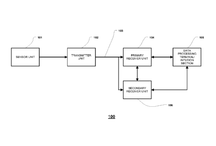
FIG. 1 illustrates a data monitoring and management system such as, for
example, analytc (e.g., glucose) monitoring system 100 in accordance with one
embodiment of the present invention. The subject invention is further
described
primarily with respect to a glucose monitoring system for convenience and such
description is in no way intended to limit the scope of the invention. It is
to be
understood that the analytc monitoring system may be configured to monitor a
variety of analytes, e.g., lactate, and the like.
Analytes that may be monitored include, for example, acetyl cholinc,
amylase, bihrubin, cholesterol, chorionic gonadotropin, creatinc kinasc (e.g.,
CK-
MB), creatine, DNA, fructosaminc, glucose, glutamine, growth hormones,
hormones, ketones, lactate, peroxide, prostate-specific antigen, prothrombin,
RNA, thyroid stimulating hormone, and troponin. The concentration of drugs,
such as, for example, antibiotics (e.g., gentamicin, vancomycin, and the
like),
digitoxin, digoxin, drugs of abuse, theophylline, and warfarin, may also be
monitored.
The analyte monitoring system 100 includes a sensor 101, a transmitter
unit 102 coupled to the sensor 101, and a primary receiver unit 104 which is
configured to communicate with the transmitter unit 102 via a communication
link
103. The primary receiver unit 104 may be further configured to transmit data
to
a data processing terminal 105 for evaluating the data received by the primary
receiver unit 104. Moreover, the data processing terminal in one embodiment
may be configured to receive data directly from the transmitter unit 102 via a
communication link 103 which may optionally be configured for bi-directional
communication.
CA 02683721 2009-10-13
WO 2008/130895
PCT/US2008/060273
-4-
Also shown in FIG. 1 is a secondary receiver unit 106 which is operatively
coupled to the communication liffl( and configured to receive data transmitted
from the transmitter unit 102. Moreover, as shown in the Figure, the secondary
receiver unit 106 is configured to communicate with the primary receiver unit
104
as well as the data processing terminal 105. Indeed, the secondary receiver
unit
106 may be configured for bi-directional wireless communication with each of
the
primary receiver unit 104 and the data processing terminal 105. As discussed
in
further detail below, in one embodiment of the present invention, the
secondary
receiver unit 106 may be configured to include a limited number of functions
and
features as compared with the primary receiver unit 104. As such, the
secondary
receiver unit 106 may be configured substantially in a smaller compact housing
or
embodied in a device such as a wrist watch, for example. Alternatively, the
secondary receiver unit 106 may be configured with the same or substantially
similar functionality as the primary receiver unit 104, and may be configured
to be
used in conjunction with a docking cradle unit for placement by bedside, for
night
time monitoring, and/or bi-directional communication device.
Only one sensor 101, transmitter unit 102, communication link 103, and
data processing terminal 105 are shown in the embodiment of the analyte
monitoring system 100 illustrated in FIG. 1. However, it will be appreciated
by
one of ordinary skill in the art that the analyte monitoring system 100 may
include
one or more sensor 101, transmitter unit 102, communication link 103, and data
processing terminal 105. Moreover, within the scope of the present invention,
the
analyte monitoring system 100 may be a continuous monitoring system, or semi-
continuous, or a discrete monitoring system. In a multi-component environment,
each device is configured to be uniquely identified by each of the other
devices in
the system so that communication conflict is readily resolved between the
various
components within the analyte monitoring system 100.
In one embodiment of the present invention, the sensor 101 is physically
positioned in or on the body of a user whose analyte level is being monitored.
The sensor 101 may be configured to continuously sample the analyte level of
the
user and convert the sampled analyte level into a corresponding data signal
for
transmission by the transmitter unit 102. In one embodiment, the transmitter
unit
102 is coupled to the sensor 101 so that both devices are positioned on the
user's
CA 02683721 2009-10-13
WO 2008/130895
PCT/US2008/060273
-5-
body, with at least a portion of the analyte sensor 101 positioned
transcutaneously
under the skin layer of the user. The transmitter unit 102 performs data
processing such as filtering and encoding on data signals, each of which
corresponds to a sampled analyte level of the user, for transmission to the
primary
receiver unit 104 via the communication link 103.
In one embodiment, the analyte monitoring system 100 is configured as a
one-way RF communication path from the transmitter unit 102 to the primary
receiver unit 104. In such embodiment, the transmitter unit 102 transmits the
sampled data signals received from the sensor 101 without acknowledgement
from the primary receiver unit 104 that the transmitted sampled data signals
have
been received. For example, the transmitter unit 102 may be configured to
transmit the encoded sampled data signals at a fixed rate (e.g., at one minute
intervals) after the completion of the initial power on procedure. Likewise,
the
primary receiver unit 104 may be configured to detect such transmitted encoded
sampled data signals at predetermined time intervals. Alternatively, the
analyte
monitoring system 100 may be configured with a bi-directional RF (or
otherwise)
communication between the transmitter unit 102 and the primary receiver unit
104.
Additionally, in one aspect, the primary receiver unit 104 may include two
sections. The first section is an analog interface section that is configured
to
communicate with the transmitter unit 102 via the communication link 103. In
one embodiment, the analog interface section may include an RF receiver and an
antenna for receiving and amplifying the data signals from the transmitter
unit
102, which are thereafter, demodulated with a local oscillator and filtered
through
a band-pass filter. The second section of the primary receiver unit 104 is a
data
processing section which is configured to process the data signals received
from
the transmitter unit 102 such as by performing data decoding, error detection
and
correction, data clock generation, and data bit recovery.
In operation, upon completing the power-on procedure, the primary
receiver unit 104 is configured to detect the presence of the transmitter unit
102
within its range based on, for example, the strength of the detected data
signals
received from the transmitter unit 102 or a predetermined transmitter
identification information. Upon successful synchronization with the
CA 02683721 2015-09-08
WO 2008/130895
PCT/US2008/060273
-6-
corresponding transmitter unit 102, the primary receiver unit 104 is
configured to
begin receiving from the transmitter unit 102 data signals corresponding to
the
user's detected analyte level. More specifically, the primary receiver unit
104 in
one embodiment is configured to perform synchronized time hopping with the
corresponding synchronized transmitter unit 102 via the communication link 103
to obtain the user's detected analyte level.
Referring again to FIG. 1, the data processing terminal 105 may include a
personal computer, a portable computer such as a laptop or a handheld device
(e.g., personal digital assistants (PDAs)), and the like, each of which may be
configured for data communication with the receiver via a wired or a wireless
connection. Additionally, the data processing terminal 105 may further be
connected to a data network (not shown) for storing, retrieving and updating
data
corresponding to the detected analyte level of the user.
Within the scope of the present invention, the data processing terminal 105
may include an infusion device such as an insulin infusion pump or the like,
which may be configured to administer insulin to patients, and which may be
configured to communicate with the receiver unit 104 for receiving, among
others,
the measured analyte level. Alternatively, the receiver unit 104 may be
configured to integrate an infusion device therein so that the receiver unit
104 is
10 configured to administer insulin therapy to patients, for example, for
administering and modifying basal profiles, as well as for determining
appropriate
boluses for administration based on, among others, the detected analyte levels
received from the transmitter unit 102.
Additionally, the transmitter unit 102, the primary receiver unit 104 and
the data processing terminal 105 may each be configured for bi-directional
wireless communication such that each of the transmitter unit 102, the primary
-
receiver unit 104 and the data processing terminal 105 may be configured to
communicate (that is, transmit data to and receive data from) with each other
via
the wireless communication link 103. More specifically, the data processing
terminal 105 may in one embodiment be configured to receive data directly from
the transmitter unit 102 via the communication link 103, where the
communication link 103, as described above, may be configured for bi-
directional
communication.
CA 02683721 2015-09-08
WO 2008/130895
PCT/US2008/060273
-7-
In this embodiment, the data processing terminal 105 which may include
an insulin pump, may be configured to receive the analyte signals from the
transmitter unit 102, and thus, incorporate the functions of the receiver 104
including data processing for managing the patient's insulin therapy and
analyte
monitoring. In one embodiment, the communication link 103 may include one or
more of an RF communication protocol, an infrared communication protocol, a
Bluctooth enabled communication protocol, an 802.11x wireless communication
protocol, or an equivalent wireless communication protocol which would allow
secure, wireless communication of several units (for example, per HIPPA
requirements) while avoiding potential data collision and interference.
FIG. 2 is a block diagram of the transmitter of the data monitoring and
detection system shown in FIG. 1 in accordance with one embodiment of the
present invention. Referring to the Figure, the transmitter unit 102 in one
embodiment includes an analog interface 201 configured to communicate with the
sensor 101 (FIG. 1), a user input 202, and a temperature detection section
203,
each of which is operatively coupled to a transmitter processor 204 such as a
central processing unit (CPU). As can be seen from FIG. 2, there are provided
four contacts, three of which are electrodes - work electrode (W) 210, guard
contact (G) 211, reference electrode (R) 212, and counter electrode (C) 213,
each
operatively coupled to the analog interface 201 of the transmitter unit 102
for
connection to the sensor unit 201 (FIG. 1). In one embodiment, each of the
work
electrode (W) 210, guard contact (G) 211, reference electrode (R) 212, and
counter electrode (C) 213 may be made using a conductive material that is
either
printed or etched, for example, such as carbon which may be printed, or metal
foil
(e.g., gold) which may be etched. Moreover, in a further aspect, the electrode
layers may be disposed in a stacked configuration where, each of the working
electrode 210, the reference electrode 212 and the counter electrode 213 may
be
disposed on a substrate layer with one or more dielectric layers disposed
therebetween such that at least a portion of each of the electrodes are
positioned
on top of one another in a stacked or layered configuration.
Further shown in FIG. 2 are a transmitter serial communication section
205 and an RF transmitter 206, each of which is also operatively coupled to
the
transmitter processor 204. Moreover, a power supply 207 such as a battery is
also
CA 02683721 2009-10-13
WO 2008/130895
PCT/US2008/060273
-8-
provided in the transmitter unit 102 to provide the necessary power for the
transmitter unit 102. Additionally, as can be seen from the Figure, clock 208
is
provided to, among others, supply real time information to the transmitter
processor 204.
In one embodiment, a unidirectional input path is established from the
sensor 101 (FIG. 1) and/or manufacturing and testing equipment to the analog
interface 201 of the transmitter unit 102, while a unidirectional output is
established from the output of the RF transmitter 206 of the transmitter unit
102
for transmission to the primary receiver unit 104. In this manner, a data path
is
shown in FIG. 2 between the aforementioned unidirectional input and output via
a
dedicated link 209 from the analog interface 201 to serial communication
section
205, thereafter to the processor 204, and then to the RF transmitter 206. As
such,
in one embodiment, via the data path described above, the transmitter unit 102
is
configured to transmit to the primary receiver unit 104 (FIG. 1), via the
communication link 103 (FIG. 1), processed and encoded data signals received
from the sensor 101 (FIG. 1). Additionally, the unidirectional communication
data path between the analog interface 201 and the RF transmitter 206
discussed
above allows for the configuration of the transmitter unit 102 for operation
upon
completion of the manufacturing process as well as for direct communication
for
diagnostic and testing purposes.
As discussed above, the transmitter processor 204 is configured to transmit
control signals to the various sections of the transmitter unit 102 during the
operation of the transmitter unit 102. In one embodiment, the transmitter
processor 204 also includes a memory (not shown) for storing data such as the
identification information for the transmitter unit 102, as well as the data
signals
received from the sensor 101. The stored information may be retrieved and
processed for transmission to the primary receiver unit 104 under the control
of
the transmitter processor 204. Furthermore, the power supply 207 may include a
commercially available battery.
The transmitter unit 102 is also configured such that the power supply
section 207 is capable of providing power to the transmitter for a minimum of
about three months of continuous operation after having been stored for about
eighteen months in a low-power (non-operating) mode. In one embodiment, this
CA 02683721 2009-10-13
WO 2008/130895
PCT/US2008/060273
-9-
may be achieved by the transmitter processor 204 operating in low power modes
in the non-operating state, for example, drawing no more than approximately 1
0_ of current. Indeed, in one embodiment, the final step during the
manufacturing process of the transmitter unit 102 may place the transmitter
unit
102 in the lower power, non-operating state (i.e., post-manufacture sleep
mode).
In this manner, the shelf life of the transmitter unit 102 may be
significantly
improved. Moreover, as shown in FIG. 2, while the power supply unit 207 is
shown as coupled to the processor 204, and as such, the processor 204 is
configured to provide control of the power supply unit 207, it should be noted
that
within the scope of the present invention, the power supply unit 207 is
configured
to provide the necessary power to each of the components of the transmitter
unit
102 shown in FIG. 2.
Referring back to FIG. 2, the power supply section 207 of the transmitter
unit 102 in one embodiment may include a rechargeable battery unit that may be
recharged by a separate power supply recharging unit (for example, provided in
the receiver unit 104) so that the transmitter unit 102 may be powered for a
longer
period of usage time. Moreover, in one embodiment, the transmitter unit 102
may
be configured without a battery in the power supply section 207, in which case
the
transmitter unit 102 may be configured to receive power from an external power
supply source (for example, a battery) as discussed in further detail below.
Referring yet again to FIG. 2, the temperature detection section 203 of the
transmitter unit 102 is configured to monitor the temperature of the skin near
the
sensor insertion site. The temperature reading is used to adjust the analyte
readings obtained from the analog interface 201. The RF transmitter 206 of the
transmitter unit 102 may be configured for operation in the frequency band of
315
MHz to 322 MHz, for example, in the United States. Further, in one embodiment,
the RF transmitter 206 is configured to modulate the carrier frequency by
performing Frequency Shift Keying and Manchester encoding. In one
embodiment, the data transmission rate is 19,200 symbols per second, with a
minimum transmission range for communication with the primary receiver unit
104.
CA 02683721 2015-09-08
WO 2008/130895
PCTPLIS2008/060273
-10-
Referring yet again to FIG. 2, also shown is a leak detection circuit 214
coupled to the guard electrode (G) 211 and the processor 204 in the
transmitter
unit 102 of the data monitoring and management system 100. The leak detection
circuit 214 in accordance with one embodiment of the present invention may be
configured to detect leakage current in the sensor 101 to determine whether
the
measured sensor data arc corrupt or whether the measured data from the sensor
101 is accurate.
Additional detailed description of the continuous analyte monitoring
system, its various components including the functional descriptions of the
transmitter are provided in U.S. Patent No. 6,175,752 issued January 16, 2001
entitled "Analyte Monitoring Device and Methods of Use", and in application
No.
10/745.878 filed December 26, 2003 entitled "Continuous Glucose Monitoring
System and Methods of Use", each assigned to the Assignee of the present
application.
Is
FIG. 3 is a block diagram of the receiver/monitor unit of the data
monitoring and management system shown in FIG. 1 in accordance with one
embodiment of the present invention. Referring to FIG. 3, the primary receiver
unit 104 includes a blood glucose test strip interface 301, an RI' receiver
302, an
20 input 303, a temperature detection section 304. and a clock 305. each of
which is
operatively coupled to a receiver processor 307. As can be further seen from
the
Figure, the primary receiver unit 104 also includes a power supply 306
operatively
coupled to a power conversion and monitoring section 308. Further, the power
conversion and monitoring section 308 is also coupled to the receiver
processor
25 307. Moreover, also shown are a receiver serial communication section
309, and
an output 310, each operatively coupled to the receiver processor 307.
In one embodiment, the test strip interface 301 includes a glucose level
testing portion to receive a manual insertion of a glucose test strip, and
thereby
determine and display the glucose level of the test strip on the output 310 of
the
30 primary receiver unit 104. This manual testing of glucose can be used to
calibrate
sensor 101. The RF receiver 302 is configured to communicate, via the
communication link 103 (FIG. 1) with the .11F transmitter 206 of the
transmitter
unit 102. to receive encoded data signals from the transmitter unit 102 fbr,
among
CA 02683721 2009-10-13
WO 2008/130895
PCT/US2008/060273
-11-
others, signal mixing, demodulation, and other data processing. The input 303
of
the primary receiver unit 104 is configured to allow the user to enter
information
into the primary receiver unit 104 as needed. In one aspect, the input 303 may
include one or more keys of a keypad, a touch-sensitive screen, or a voice-
activated input command unit. The temperature detection section 304 is
configured to provide temperature information of the primary receiver unit 104
to
the receiver processor 307, while the clock 305 provides, among others, real
time
information to the receiver processor 307.
Each of the various components of the primary receiver unit 104 shown in
FIG. 3 is powered by the power supply 306 which, in one embodiment, includes a
battery. Furthermore, the power conversion and monitoring section 308 is
configured to monitor the power usage by the various components in the primary
receiver unit 104 for effective power management and to alert the user, for
example, in the event of power usage which renders the primary receiver unit
104
in sub-optimal operating conditions. An example of such sub-optimal operating
condition may include, for example, operating the vibration output mode (as
discussed below) for a period of time thus substantially draining the power
supply
306 while the processor 307 (thus, the primary receiver unit 104) is turned
on.
Moreover, the power conversion and monitoring section 308 may additionally be
configured to include a reverse polarity protection circuit such as a field
effect
transistor (FET) configured as a battery activated switch.
The serial communication section 309 in the primary receiver unit 104 is
configured to provide a bi-directional communication path from the testing
and/or
manufacturing equipment for, among others, initialization, testing, and
configuration of the primary receiver unit 104. Serial communication section
104
can also be used to upload data to a computer, such as time-stamped blood
glucose data. The communication liffl( with an external device (not shown) can
be
made, for example, by cable, infrared (IR) or RF link. The output 310 of the
primary receiver unit 104 is configured to provide, among others, a graphical
user
interface (GUI) such as a liquid crystal display (LCD) for displaying
information.
Additionally, the output 310 may also include an integrated speaker for
outputting
audible signals as well as to provide vibration output as commonly found in
handheld electronic devices, such as mobile telephones presently available. In
a
CA 02683721 2009-10-13
WO 2008/130895
PCT/US2008/060273
-12-
further embodiment, the primary receiver unit 104 also includes an electro-
luminescent lamp configured to provide backlighting to the output 310 for
output
visual display in dark ambient surroundings.
Referring back to FIG. 3, the primary receiver unit 104 in one embodiment
may also include a storage section such as a programmable, non-volatile memory
device as part of the processor 307, or provided separately in the primary
receiver
unit 104, operatively coupled to the processor 307. The processor 307 is
further
configured to perform Manchester decoding as well as error detection and
correction upon the encoded data signals received from the transmitter unit
102
via the communication link 103.
In a further embodiment, the one or more of the transmitter unit 102, the
primary receiver unit 104, secondary receiver unit 105, or the data processing
terminal/infusion section 105 may be configured to receive the blood glucose
value wirelessly over a communication link from, for example, a glucose meter.
In still a further embodiment, the user or patient manipulating or using the
analyte
monitoring system 100 (FIG. 1) may manually input the blood glucose value
using, for example, a user interface (for example, a keyboard, keypad, and the
like) incorporated in the one or more of the transmitter unit 102, the primary
receiver unit 104, secondary receiver unit 105, or the data processing
terminal/infusion section 105.
FIG. 4 is a schematic of the dynamic multi-stage signal amplification in
the transmitter unit of the data monitoring and management system shown in
FIG.
1 in accordance with one embodiment of the present invention. Referring to
FIG.
4, there is provided in one embodiment a transimpedance amplifier 420 whose
output terminal 423 is coupled to a first input terminal 411 of the analog to
digital
converter (ADC) 410 in the analog interface 201 (FIG. 1) of the transmitter
unit
102. Further shown in FIG. 4, the monitored analyte sensor signal from the
sensor
unit 101 is provided to an inverting input terminal 421 of the transimpedance
amplifier 420. The sensor signal in FIG. 4 is shown as a signal source 440.
Furthermore, a noninverting input terminal 422 of the transimpedance amplifier
420 is provided with a reference voltage signal from a reference signal source
Vref 450. In one embodiment, the reference voltage signal may be approximately
CA 02683721 2015-09-08
WO 2008/130895
PCT/US2008/060273
-13-
1.012 volts. However, based upon the component tolerance, and design
configuration, other suitable reference voltage signals may be used.
In one aspect, based on the input analyte sensor signal from the signal
source 440 and the reference signal Vref 450, the transimpedance amplifier 420
may be in one embodiment configured to convert the received current signal
representing the monitored or detected analyte level, and to convert the
current
signal to a corresponding voltage signal which is provided to the output
terminal
423 of the transimpedance amplifier 420. Further, as shown in FIG. 4 the
monitored analyte voltage signal from the output terminal 423 of the
transimpedance amplifier 420 is provided to the first input terminal 411
(Channel
1) of the ADC 410.
Referring again to FIG. 4, a second amplifier 430 is provided in one
embodiment whose noninverting input terminal 431 is coupled to the output
terminal 423 of the transimpedance amplifier 420 to receive the output voltage
signal corresponding to the monitored analyte level, while an inverting input
terminal 432 of the second amplifier 430 is coupled in one embodiment to the
reference signal Vref source 450. Moreover, output terminal 433 of the second
amplifier is coupled in one embodiment to a second input terminal 412 (Channel
2) of the ADC 410. In operation, the second amplifier 430 may be configured to
step up the output signal of the transimpedance amplifier 410 by a
predetermined
factor (for example, a factor of 2), and to provide the stepped up signal to
the
analog to digital converter (ADC) 410.
Referring back to FIG. 4, the analog to digital converter (ADC) 410 of the
analog interface 201 (FIG. 2) of the transmitter unit 102 (FIG. 1) in one
embodiment may be configured to detect signals at both the first and second
input
terminals or channels 411, 412, and based on one or more predetermined
processing or routine, the voltage signal at one of the first or the second
input
terminals or channels 411, 412 is used by the ADC 410 for further processing
as
corresponding to the monitored analyte level from the sensor unit 101 (FIG.
1).
That is, in one embodiment, depending upon the signal resolution corresponding
to the analyte level monitored, the ADC 410 may be configured to select one of
the output signals from the transimpedance amplifier 420 or the second
amplifier
430 for further processing.
CA 02683721 2015-09-08
WO 2008/130895
PCT/US2008/060273
-14-
For example, when the signal received at the second input terminal 412 of
the ADC 410 exceeds a predetermined threshold value, the input signal at the
first
input terminal 411 may be used. More specifically, in one embodiment, the ADC
410 may be configured to process the signals at the second input terminal 412
(Channel 2) since it has a higher resolution compared to the signal at the
first
input terminal 411 received from the transimpedance amplifier 420. When the
signal received at the second input terminal 412 exceeds a predetermined
threshold level (for example, based on the tolerance level of the analog to
digital
converter (ADC) 410), the voltage signal received at the first input terminal
411
from the transimpedance amplifier 420 may be used to convert to a
corresponding
digital signal representing the monitored analyte level detected by the sensor
unit
101 (FIG. 1).
Referring back to FIG. 4, in one embodiment, the analog to digital
converter (ADC) 410 may include a 12 bit AID converter configured to support
up
to approximately 4,096 bits or ADC counts. In this case, in one embodiment,
when the signal at the second input terminal 412 of the ADC 410 approaches
approximately 4,000 bits or ADC counts, for example, the processor 204 (FIG.
2)
of the transmitter unit 102 may be configured to switch from the second input
terminal 412 to the first input terminal 411, to use the output signal from
the
transimpedance amplifier 420. In this manner, in one embodiment, the processor
204 of the transmitter unit 102 may be configured to monitor the signal levels
at
the two input terminals 411,412 of the ADC 410, and when the signal level or
ADC count associated with the output signal from the second amplifier 430
provided at the second input terminal 412 of the ADC 410 exceeds the
predetermined threshold (for example, 4,000 bits or ADC count), the processor
204 may be configured to switch over to the output signal of the
transimpedance
amplifier 410 provided on the first input terminal 411 of the ADC 410 for
further
processing.
In the manner described above, the dynamic multi-stage amplifier
configuration in one embodiment may be configured to support variations in the
analyte sensor sensitivities due to, for example, manufacturing variations,
among
others, while maintaining an acceptable or desirable sensor signal resolution.
For
example, in one embodiment, high sensitivity sensors may be configured for use
CA 02683721 2009-10-13
WO 2008/130895
PCT/US2008/060273
-15-
with the full scale or range (for example, up to approximately 150 nA
corresponding to the supported approximately 500mg/dL glucose level)
associated
with the transimpedance amplifier 420 output signal provided to the first
input
terminal (channel 1) 411 of the analog to digital converter (ADC) 410, while
low
sensitivity sensors may be associated with the second amplifier 430 output
signal
(for example, full scale current signal level of approximately 75 nA
corresponding
to the supported approximately 500 mg/dL glucose level) provided to the second
input terminal (channel 2) 412 of the analog to digital converter (ADC) 410.
For example, as discussed above, in one embodiment, the processor 204 of
the transmitter unit 102 may be configured to monitor the signals at the two
input
terminals 411, 412 of the ADC 410, and determine, that if the received signal
level does not have sufficient resolution to convert to the desired resolution
of the
digital signal (for example, 12 bits for the ADC 410) corresponding to the
monitored analyte level associated with the sensor unit 101, the processor 204
may be configured to dynamically toggle or switch from using the voltage
signal
received from one of the two input terminals 411, 412, to using the voltage
signal
from the other one of the two input terminals 411, 412 to provide a dynamic
range
of tolerance level for the sensor sensitivities.
Accordingly, an apparatus in one embodiment includes a first amplifier
having at least one input terminal and an output terminal, the at least one
input
terminal coupled to a signal source, the output terminal configured to provide
a
first output signal, a second amplifier having at least one input terminal and
an
output terminal, the at least one input terminal coupled to the output
terminal of
the first amplifier, the output terminal of the second amplifier configured to
provide a second output signal, a processor operatively coupled to receive the
first
output signal and the second output signal, where the first output signal is a
predetermined ratio of the second output signal, and further, where the first
output
signal and the second output signal are associated with a monitored analyte
level
of a user.
In one aspect, the first amplifier may include a transimpedance amplifier.
The monitored analyte level may include glucose level.
CA 02683721 2009-10-13
WO 2008/130895
PCT/US2008/060273
-16-
Also, the at least one input terminal of the first amplifier may include an
inverting input terminal, and, also may provided is a reference signal source
coupled to a noninverting input terminal of the first amplifier.
In a further aspect, the second amplifier may include a gain of
approximately two.
In still another aspect, the first output signal may be associated with a
signal level from the signal source.
The apparatus may also include an analog to digital converter coupled to
the output terminals of the first and second amplifiers, where the analog to
digital
(AID) converter may include a 12 bit AID converter.
The apparatus in another embodiment may include a processor operatively
coupled to the AID converter for processing the one or more signals received
at
the one or more first amplifier output terminal and the second amplifier
output
terminal.
Moreover, the processor may be configured to compare the one or more
signals received at the one or more first amplifier output terminal and the
second
amplifier output terminal to a predetermined threshold value, which, in one
embodiment may include approximately 4,000 bits (or analog to digital
converter
(ADC) counts)).
Still further, the processor may be configured to process a signal
associated with one of the one or more signals received at the one or more
first
amplifier output terminal and the second amplifier output terminal when
another
signal associated with the other one of the one or more signals received at
the one
or more fist amplifier output terminal and the second amplifier output
terminal
exceeds the predetermined threshold value.
A method in accordance with another embodiment includes receiving a
first signal having a first signal resolution and associated with a monitored
analyte
level of a user, receiving a second signal having a second signal resolution
and
associated with the monitored analyte level of the user, comparing the
received
first signal to a predetermined threshold level, and processing one of the
received
first or the second signals based on the comparing step.
When the received first signal does not exceed the predetermined threshold
level, further including processing the first signal. On the other hand, when
the
CA 02683721 2016-03-04
-17-
received first signal exceeds the predetermined threshold level, further
including
processing the second signal.
A data processing device in accordance with still another embodiment
includes a multi stage amplifier unit configured to receive a signal and to
generate
a plurality of amplifier unit output signals each corresponding to a monitored
analyte level of a patient, an analog to digital (AID) conversion unit
operatively
coupled to the multi-stage amplifier unit configured to digitally convert the
plurality of amplifier unit output signals, and a processor unit operatively
coupled
to the AID conversion unit, the processor unit configured to process one of
the
plurality of digitally converted amplifier unit output signals.
The device in another aspect may include a data communication unit
operatively coupled to the processor unit, and configured to transmit the
digitally
converted and processed amplifier unit output signal.
The data communication unit may include an RF transmitter for wireless
data transmission to a remote device such as, for example, a data receiver
unit,
data processing terminal, an infusion device or the like configured for RF
communication.
Various other modifications and alterations in the structure and method of
operation of this invention will be apparent to those skilled in the art
without
departing from the scope of the invention. Although the invention has
been described in connection with specific preferred embodiments, it should be
understood that the invention as claimed should not be unduly limited to such
specific embodiments. The scope of the claims should not be limited by the
preferred embodiments set forth in the examples, but should be given the
broadest
26 interpretation consistent with the description as a whole.