Note: Descriptions are shown in the official language in which they were submitted.
CA 02684045 2009-10-27
CNN-028638 CA
METHOD AND APPARATUS FOR STIMULATING
POWER LINE CARRIER INJECTION WITH
REACTIVE OSCILLATION
TECHNICAL FIELD
[0001] The present invention relates generally to the field of power line
carrier
communications, and more particularly to methods and systems for stimulating
power line
carrier injection with reactive oscillation.
BACKGROUND
[0002] Injecting power line carrier signals onto power lines for the purpose
of communicating
digital data from one location to another is used in the field of power
distribution. Typically, a
power line carrier signal is generated by supplying a sinusoidal signal at the
input of an
amplifier. The signal is amplified and then injected onto the power line by
injecting it into the
secondary winding of a power transformer that is connected to the power line
or injecting it
directly onto the power line through high voltage capacitors. In the case of
the transformer type
injection, the signal that is injected into the secondary winding of the
transformer induces a
signal on the primary winding of the transformer which is connected to the
power line. Digital
data is communicated by modulating the phase of the carrier signal that is
induced onto the
power line.
[0003] For conventional power line carrier infrastructure, large capacitors
may be used to
couple the carrier signal onto the distribution lines. These large capacitors
can be a safety
concern as they are at distribution line potential (7.5 to 25kV) and can store
an electrical charge
for a long period of time.
[0004] Another disadvantage of conventional power line carrier injecting
systems is the
complexity of the circuitry in such systems. The complexity of the circuitry
can lead to higher
manufacturing and maintenance costs.
[0005] Accordingly, a need exists within the art for a power line carrier
injection device that
can reduce or eliminate the use of large coupling capacitors and/or complex
circuitry, that can
1
CA 02684045 2009-10-27
CNN-028638 CA
increase the safety of the device, and/or that can allow for the device to be
installed in a smaller
enclosure.
SUMMARY
[0006] The present invention can make it possible to stimulate power line
carrier signals
without a large power supply or large capacitor to couple the carrier signal
onto the power line.
The present invention utilizes short pulses of current to excite a tank
circuit and therefore force
the tank circuit to oscillate at the frequency of excitation, which can be
near the natural resonant
frequency of the tank circuit. This process allows the carrier signal to be
coupled onto the
distribution lines through the power transformer.
[0007] In one aspect of the present invention, a power transformer is
connected to a
distribution system to provide power to a circuit and to allow stimulated
power line carrier signal
to be coupled onto the distribution system. An excitation circuit sinks short
pulses of current
between a first node of a capacitor and a second node of a capacitor that is
connected in a tank
circuit arrangement with an inductor and the secondary winding of the power
transformer. The
tank circuit oscillates at the frequency of the excitation pulses when pulses
of current are sunk at
a frequency close to the resonant frequency of the tank circuit. The
oscillating current is coupled
onto the power line system through the power transformer. The phase of the
power line carrier is
shifted by shifting the phase of the excitation pulses.
[0008] In another aspect of the present invention, a current sensor measures
current flowing
through a field effect transistor (FET) that is included in the excitation
circuit. A FET control
circuit controls the amount of current flowing through the FET by adjusting
the voltage at a gate
node of the FET.
[0009] These and other aspects, objects, features, and embodiments of the
present invention
will become apparent to those having ordinary skill in the art upon
consideration of the following
detailed description of illustrative embodiments exemplifying the best mode
for carrying out the
invention as presently perceived.
2
CA 02684045 2009-10-27
CNN-028638 CA
BRIEF DESCRIPTION OF THE DRAWINGS
[0010] Figure 1 is a functional block diagram illustrating a method for
stimulating power line
carrier injection with reactive oscillation according to an exemplary
embodiment of the present
invention.
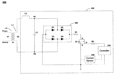
[0011] Figure 2 is a schematic illustration of a circuit for stimulating power
line carrier
injection with reactive oscillation according to an exemplary embodiment of
the present
invention.
DETAILED DESCRIPTION OF EXEMPLARY EMBODIMENTS
[0012] The present invention provides methods and systems for stimulating
power line
carrier injection. Specifically, the invention provides methods and systems
for stimulating power
line carrier injection using reactive oscillation. This method can reduce or
eliminate the need for
large coupling capacitors and/or complex circuitry.
[0013] Turning now to the drawings, in which like numerals indicate like
elements
throughout the figures, exemplary embodiments of the invention are described
in detail.
[0014] Figure 1 illustrates a method 100 for stimulating power line carrier
injection with
reactive oscillation according to an exemplary embodiment of the present
invention. Figure 1
will be described with reference to Figure 2, which illustrates a circuit 200
for stimulating power
line carrier injection with reactive oscillation according to an exemplary
embodiment of the
present invention.
[0015] Step 110 begins the excitation process.
[0016] In step 115, a power transformer T1 connected to a distribution system
(not shown)
serves to provide power to a power line carrier stimulating device 230 and to
couple a carrier
signal to the distribution system. The power transformer T1 has a primary
winding L3 and a
secondary winding L1. The primary winding L3 of the power transformer Ti is
connected
across a single phase of the power line system and the neutral line of the
power line system such
that an AC voltage is developed across the primary winding U. Although this
exemplary
3
CA 02684045 2009-10-27
CNN-028638 CA
embodiment is described with reference to a single phase of the power line
system, poly-phase
configurations also are possible using the method described herein.
[0017] In a typical application, the power transformer T1 steps the primary
voltage Vl on
the primary winding L3 down to a lower voltage V2 on the secondary winding L1,
or
alternatively, the power transformer Tl steps the secondary voltage V2 on the
secondary
winding L1 up to the voltage Vl on the primary winding U. For example, the
primary voltage
Vl may be greater than 1 Kilovolt (KV) and the secondary voltage V2 may be 240
Volts (V).
[0018] In step 120, with power provided to the power line carrier stimulating
device 230, the
device may begin generating excitation pulses.
[0019] To inject power line carrier signals onto the distribution system, a
tank circuit, is
forced to oscillate. The tank circuit comprises the secondary winding L1, an
inductor L2, and a
capacitor C1. One method of exciting the tank circuit and therefore forcing
the tank circuit to
oscillate is to sink short pulses of current between one node of the capacitor
Ci and the other
node of the capacitor C1. The capacitor nodes are represented in Figure 2 by
nodes Nl and N2.
If the resonant frequency of the tank circuit is relatively close (within a
few kHz) to the
frequency of the excitation, the tank circuit will oscillate at the frequency
of the excitation
pulses. Also, changing the phase of the excitation pulses will cause the same
phase change in the
oscillations of the tank circuit. This process allows many types of Phase
Shift Keying to be
possible.
[0020] An excitation circuit is utilized to sink short pulses of current
between nodes N1 and
node N2. In this exemplary embodiment, the excitation circuit includes a FET
Q1, a controller
210, two resistors Rl and R3, a full wave rectifier 220, and a current sensor
215 configured as
depicted in Figure 2. Alternative exemplary embodiments may include multiple
FETs and other
components to refine the power line carrier signal.
[0021] In step 125, the channel between the source S and drain D of the FET Q1
is opened to
sink pulses of current between node Nl and node N2. This task is accomplished
by applying a
suitable voltage to the gate G of the FET Qi to open the channel. The level of
voltage required
4
CA 02684045 2009-10-27
CNN-028638 CA
depends upon the FET chosen and the other components included in the circuit.
In one
exemplary embodiment, the voltage is supplied by a microcontroller included in
the controller
210. The controller determines the correct voltage to apply to the gate G of
the FET Q1 based
on the current sensor feedback. In an exemplary embodiment, the
microcontroller can apply
voltage to and remove voltage from the gate G of the FET repeatedly at a
specified frequency,
similar to a square wave.
[0022] After the channel between the source S and the drain D of the FET Q1 is
opened, the
electrical charge stored in the capacitor Cl will discharge through the
excitation circuit. As
discussed previously, the exemplary excitation circuit comprises the Field
Effect Transistor
(FET) Q1, the controller 210, two resistors Rl and R3, the full wave rectifier
220, and the
current sensor 215 configured as depicted in Figure 2. The rectifier circuit
220 is connected
between nodes N1 and N2 to allow current to flow through the FET Q1 regardless
of the polarity
of the power line voltage. If the voltage at N1 is greater than the voltage at
node N2, current will
flow from the node of the capacitor C1 connected to node N1 through diode D2,
resistor Ri, the
drain D of FET Q1, the source S of FET Q1, and finally through diode D3 to
reach node N2. If
the voltage at N2 is greater than the voltage at node N1, current will flow
from the node of the
capacitor C1 connected to node N2 through diode D4, resistor Rl, the drain D
of FET Q1, the
source S of FET Q1, and finally through diode D1 to reach node N1.
[0023] In an exemplary embodiment, the channel is held open for less than 50%
of the period
of the desired power line carrier frequency. The amplitude of the output
signal can vary with a
change in the pulse width, or duty cycle. For a duty cycle of up to about 50%
of the period of the
carrier frequency, the amplitude increases with an increase in duty cycle. The
amplitude of the
output signal tends to decrease with an increase of duty cycle above
approximately 50% of the
carrier frequency.
[0024] In the exemplary embodiment illustrated in Figure 2, the resistor Rl
can be included
in the circuit between the rectifier 220 and the drain D of the FET Q1 to
dissipate some of the
power that is flowing through the excitation circuit. If a higher resistance
of Rl is chosen, the
resistor Rl will dissipate more power and decrease the power requirements of
the FET Q1. A
CA 02684045 2009-10-27
CNN-028638 CA
lower resistance of Rl allows for greater output power but would require a
higher power
requirement of the FET Q1.
[0025] In step 130, a current sensor 215 measures the current flowing through
the source S
and drain D of the FET Q1. In one exemplary embodiment, the current sensor 215
includes a
low resistance resistor (for example, approximately 50 mS2) connected between
the source S of
the FET Ql and ground. Then, the voltage across the resistor can be amplified
and compared to
a reference voltage in the controller' 210 to determine if the amount of
current flowing through
the source S and drain D of the FET Ql is at a desired level.
[0026] In step 135, the controller 210 adjusts the level of current flowing
through the source
S and drain D of the FET Q1 based on the current measurement obtained in step
130. In an
exemplary embodiment, the controller 210 includes a FET control circuit (not
shown) that
adjusts the current flowing through the FET Ql by adjusting the voltage at the
gate G of the FET
Q1. The level of voltage at the gate G of the FET Q1 can control the size of
the channel
between the source S and drain D of the FET Q1, thus allowing more or less
current to flow
through the channel. A typical FET control circuit includes an operational
amplifier, resistors to
set the gain of the operational amplifier, and one or more capacitors to
filter the output signal.
[0027] The use of a FET control circuit and the current sensor 215 allows the
controller 210
to maintain a constant current flow through the source S and drain D of the
FET Ql. This
method prevents damage to the device by reducing current through Ql and also
serves to provide
more consistent carrier output. Alternatively, a voltage divider network can
be employed at the
gate G of the FET Q1 to maintain a consistent voltage level at the gate G of
the FET Q1. This
method may not provide a consistent current flow through the source S and
drain D of the FET
Q1 but will still excite the tank circuit.
[0028] In step 140, if the duty cycle has not expired, the method returns to
step 130 to
measure the current flowing through the FET Q1. If the duty cycle has expired,
the method
proceeds to step 145.
6
CA 02684045 2009-10-27
CNN-028638 CA
[0029] In step 145, the channel between the source and drain of FET Q1 is
closed by
removing or reducing the voltage at the gate G of the FET Q1.
[0030] In step 150, the excitation pulse generated in step 125 causes the tank
circuit to
oscillate at the frequency of the excitation pulses. The tank circuit includes
the secondary
winding L1 of the power transformer T1, the inductor L2, and the capacitor Cl.
As discussed
above, the resonant frequency of the tank circuit can be close to the
frequency of the carrier
signal. The resonant frequency (f) for the tank circuit in Figure 2 is
calculated using formula [1]
below, where L is the combined inductance of L1 and L2 in Henries and C is the
capacitance of
Cl in Farads.
_ 1 1
f 2;r LC [ ]
[0031] The capacitor Cl and the inductor L2 values are chosen to give the
resulting tank
circuit a resonate frequency that is close to the power line carrier
frequency. In an exemplary
embodiment, the capacitor Cl and the inductor L2 can be onboard and/or within
the enclosure of
the power line carrier generation device that contains the excitation circuit.
In certain exemplary
embodiments, more than one inductor and more than one capacitor may be used in
the tank
circuit. Other components can be utilized in the tank circuit as well.
[0032] When the voltage across the capacitor Cl differs from the voltage
across the
secondary winding of the transformer T1 (usually due to the excitation
pulses), the capacitor Cl
begins to recharge by sinking current out of the transformer T1 through the
inductor L2. When
the voltage across the capacitor Cl reaches the voltage of the secondary
winding of the
transformer T1, the inductance in the secondary winding of the transformer T2
and the inductor
L2 force the capacitor C1 to overcharge to a voltage greater than the voltage
across the
secondary winding of the transformer T2. This process is responsible for the
oscillatory
behavior of the device.
7
CA 02684045 2009-10-27
CNN-028638 CA
[0033] In step 155 , the oscillation of current flows through the secondary
winding L1 of the
power transformer T1 and couples the carrier signal onto the primary side of
the power
transformer and thus onto the distribution system.
[0034] In step 160, until it is desired to stop injecting power line carrier
signals onto the
power line system, the method 100 returns to step 120 and continues sinking
pulses of current
between one node of capacitor Cl and the other node of capacitor Cl to
oscillate the tank circuit
and to induce power line carrier signals onto the distribution system.
[0035] Although the functional block diagram 100 illustrates steps 125-145
occurring after
step 115 and before steps 150 and 155, steps 125-145, step 115, and steps 150
and 155 are
typically executing in parallel after steps 125-145 have executed for the
first time. Accordingly,
these steps may be performed simultaneously or in an alternative order.
[0036] Without any additional pulses of current, the tank circuit would
oscillate at the
resonant frequency of the tank circuit until the overall resistance of the
tank circuit causes the
oscillation of current to decay. When pulses of current are sunk at or near
the resonant frequency
of the tank circuit, each pulse builds on the previous pulses to maintain the
oscillation of current.
For example, the second pulse of current builds on the second oscillation
caused by the first
pulse of current.
[0037] Phase Shift Keying can be accomplished by adjusting the phase of the
excitation
pulses. In an exemplary application, the frequency of the power line carrier,
and therefore the
frequency that the excitation pulses should be applied is 12.5 kHz. The period
of a 12.5 kHz
signal is 80 microseconds ( s). A 180 phase shift can be accomplished by
either shortening the
period between one pulse and the next pulse fr6m 80 s to 40 s or by
lengthening the period
between one pulse and the next pulse from 80 s to 120 s.
[0038] One of ordinary skill in the art will appreciate that the present
invention provides
methods and systems for stimulating power line carrier injection.
Specifically, the invention
provides methods and systems for stimulating power line carrier injection
using reactive
oscillation. This method can eliminate or reduce the need for a large coupling
capacitor and/or
8
CA 02684045 2009-10-27
CNN-028638 CA
complex circuitry. Many other modifications, features, and embodiments of the
invention will
become evident to those having ordinary skill in the art. It should be
appreciated, therefore, that
many aspects of the invention were described above by way of example only and
are not
intended as required or essential elements of the invention unless explicitly
stated otherwise.
Accordingly, it should be understood that the foregoing description relates
only to certain
exemplary embodiments of the invention and that numerous changes may be made
therein
without departing from the spirit and scope of the invention as defined by the
following claims.
It should also be understood that the invention is not restricted to the
illustrated embodiments
and that the various modifications can be made within the scope of the
following claims.
9