Note: Descriptions are shown in the official language in which they were submitted.
CA 02684394 2009-10-16
WO 2008/128726
PCT/EP2008/003150
- 1 -
Highly conductive, transparent carbon films as
electrode materials
Description
The present invention relates to an optically transparent conductive carbon-
based film, a process for the production thereof and the application of the
film as electrode in optoelectronic devices.
Optically transparent electrodes consisting of thin conductive films which
are deposited on transparent substrates have been the subject of intense
research. These film systems are of particular interest for use in for example
flat panel displays, photovoltaic cells, electrochromic devices,
electroluminescent lamps and a large number of further applications. For
these applications, transparent electrodes must exhibit three important
qualities: high optical transparency, electrical conductivity and mechanical
durability.
The most commonly used material in optically transparent conductive films
is indium-tin oxide (ITO). However, due to the high cost and limited supply
of indium, alternatives are being sought for modern optoelectronic
devices. So far, development of different inorganic and polymer layers as
well as films of carbon nanotubes has been investigated. The use of carbon
materials is particularly attractive since carbon is easily available, cheap
and inert. The low electrical resistance and at the same time high optical
transparency are essential for good application properties of carbon films.
These two properties, however, are oppositely influenced by the film
thickness. Films had to be sufficiently thick to provide low electrical
resistance for reasonable electrochemical properties, yet had to be
sufficiently thin to maintain high optical transparency. The layer thickness
was chosen to obtain a compromise between the two desired properties.
Carbon has been used as an electrode material for a range of
CA 02684394 2009-10-16
WO 2008/128726
PCT/EP2008/003150
- 2 -
applications. The popularity can be traced to the versatility and
availability of many types of carbon which can easily be fabricated into
electrodes. Carbon materials also provide renewable and reproducible
surfaces as well as low chemical reactivity.
Carbon-based optically transparent electrodes (OTEs) have been
developed for spectroelectrochemical studies (Matthias Kummer and
Jon R. Kirchhoff, Anal. Chem. (1993), 65, 3720-3725). Pyrolytic graphite-
coated electrodes were prepared by vapor deposition of acetone as carbon
precursor onto resistively heated metal mesh substrate, whereby a thin
layer of graphite was deposited on the heated metal mesh.
Another approach was the provision of reticulated vitreous carbon
electrodes (Janet Weiss Sorrels and Howard D. Dewald, Anal. Chem.
(1990), 62, 1640-1643). Reticulated vitreous carbon (RVC) is a porous,
vitreous carbon foam material. For use as electrodes it is sliced to slides
having a thickness of about 0.5 to 3.5 mm.
Further, carbon optically transparent electrodes have been prepared by
vapor deposition of a thin carbon film on a glass or quartz substrate (J.
Mattson et al., Anal. Chem. (1995) Vol. 47 No. 7, 1122-1125; T.P.
DeAngelis et al., Anal. Chem. (1977), Vol. 49, No. 9, 1395-1398). The
carbon was evaporated by an electron beam technique using a glassy
carbon source and the evaporated carbon was then deposited as carbon
film onto substrates.
Further, optically transparent carbon film electrodes were prepared by
forming a carbon film on a quartz substrate by a vacuum pyrolysis of 3, 4, 9,
10-perylenetetracarboxylic dianhydride (D. Anjo et al., Anal. Chem. (1993),
65, 317-319). The carbon source 3, 4, 9, 10-perylenetetracarboxylic
dianhydride was sublimed and then vapor-pyrolized at 800 C on the surface
of a quartz substrate producing a mirror-like conductive coating.
CA 02684394 2009-10-16
WO 2008/128726
PCT/EP2008/003150
- 3 -
EP 1 063 196 describes a carbonaceous complex structure comprising a
layered set of a substrate, a carbonaceous thin film and a fullerene thin
film.
The films are obtained by thermally decomposing carbon compounds such
as fullerene molecules or organic solvents, such as ethanol or toluene. The
conductivity of the carbonaceous films described in EP 1 063 196 is in the
order to 10-2S/cm. Such a low conductivity, however, is not sufficient to
make the carbonaceous film of EP 1063196 suitable as a transparent
electrode in optoelectronic devices, such as solar cells.
Donner et al., (Anal. Chem. (2006) Vol. 78, No. 8, 2816-2822) describe the
preparation of carbon-based optically transparent electrodes fabricated by
pyrolysis of thin films of photoresists. The photoresist AZ 4330 was spin
coated onto quartz substrates and a carbon film was produced by pyrolysis
in a reducing atmosphere. The photoresist AZ 4330 is a cresol-novolak
resin with highly branched structures and the reaction of this polymer with
diazonaphthoquinonosulfonic esters results in a hard amorphous carbon
structure. The films obtained by this course of action show a low
transparency, for example a transparency of only 47% for a 13 nm thick
carbon film. Such low transparency cannot meet the demand of modern
optoelectronic devices.
As we know, a compromise between electrical resistance and optical
transparency had to be accepted with all known methods due to their
dependence on the carbon film thickness. Generally, resistance of carbon
films undergoes a dramatic increase as thickness decreases below
around 30 nm. Therefore, hitherto reported carbon films even in the
thickness of -13nm, with sheet resistance in the range of 1000-2000 ohm/
sq, have transmittance lower than 55%. Since these reported carbon film
electrodes were only used in spectroelectrochemical studies, such
transparency was enough. However, such low transparency cannot meet
demand of modern devices such as optoelectronic devices. Besides high
transparency, modern devices require transparent electrodes with low
resistance, smooth surface as well as suitable work function which depends
strongly on the structure of carbon film. Obviously, the type of precursor and
CA 02684394 2014-11-12
- 4 -
preparing methods are important for fabrication of structure-controllable
carbon films. Furthermore, most of the reported methods for preparing
transparent carbon films are complicated.
The art therefore seeks suitable precursors and simple procedures for
making highly transparent, conductive and structure-controllable carbon films
with smooth surface and appropriate work function for modern device
application, in particular for use in optoelectronic devices.
SUMMARY OF INVENTION
The object of the present invention is therefore to provide a thin highly
trans-
parent and conducting carbon film which also has suitable work function for
optoelectronic devices. A further object was to provide such a carbon film in
an easy, cheap and reproducible way.
This object of the invention is solved by a method for the production of a
transparent conductive carbon film comprising the steps (i) coating of a
solution of discotic precursors onto a substrate and (ii) heating the coated
substrate under a protective gas to a temperature of from 400-2000 C.
The invention provides a simple, cheap and reliable method producing
optically transparent conductive carbon films. In the inventive process, the
thickness of the carbon film produced can easily be controlled by
concentration of the solution of discotic precursors or by the repetition of
the
steps (i) and (ii). Further, the size of the film sheets is only limited by
the size
of the substrates used. Further, the carbon film obtained according to the
inventive process has a higher thermal and chemical stability than
traditionally used ITO. Further, it has an extremely smooth surface, which
can e.g. not be obtained with carbon nanotube films. With the inventive
method, it is possible to provide conductive carbon films having both a high
transparency and at the same time a low electrical resistance.
CA 02684394 2014-11-27
- 4a -
In accordance with one aspect of the present invention, there is provided a
method for the production of a transparent conductive carbon film comprising
the steps (i) coating of a solution of discotic precursors onto a substrate,
and
(ii) heating the coated substrate under an inert gas to a temperature of from
400-2000 C, wherein the produced transparent carbon film has a
transmittance in the range of 60-95%, for a carbon film having a thickness of
30 nm ¨4 nm at a wave length of 700 nm, wherein the produced carbon film
has a sheet resistance at most 30 kohm/sq, and wherein the discotic
precursors are selected from superphenalenes, hexabenzochoronenes
(HBC), ovalenes, coronenes, perylenes, pyrenes, and their derivatives;
pitches, heavy oils from coal or petroleum; or exfoliated graphite from
chemical or physical exfoliation of any graphite or from graphite oxide.
In accordance with another aspect of the method herein described, the
discotic precursors are selected from oligo- or polycyclic aromatic
hydrocarbons having at least three aromatic rings.
In accordance with yet another aspect of the method herein described, the
noble gas is Ar.
In accordance with still another aspect of the method herein described, in
step (i) flat-aligned discotic structures are formed.
In accordance with yet still another aspect of the method herein described,
characterized in that a linkage of the flat-aligned discotic structures is
effected by heating.
In accordance with a further aspect of the method herein described,
characterized in that in step (ii) the temperature is slowly increased so that
no melting of the discotic precursors is effected.
In accordance with yet a further aspect of the method herein described,
characterized in that the heating is conducted at a heating rate of less than
or equal to 10 C/min.
CA 02684394 2014-11-12
- 4b -
The transmittance of the carbon film produced is preferably at least 50%,
more preferably at least 70%. Generally, the transmittance of the carbon film
in in the range of 60-95%. The transmittance of a material is dependent on
the respective wave length. The transmittance values indicated herein refer
CA 02684394 2009-10-16
WO 2008/128726
PCT/EP2008/003150
- 5 -
to a wave length of 500-800 nm, particularly to a wave length of 600-700
nm, and particularly to a wave length of 700 nm, unless otherwise noted.
Further, the transmittance is dependent on the film thickness. The
transmittance values indicated herein refer to a film thickness of < 50 nm,
s
particularly 5_ 30 nm and 5 nm, in particular 10 > nm and in particular to a
film thickness of 30 nm unless otherwise noted.
Unlike carbon-based films of the prior art, the sheet resistance of the carbon
films of the invention is quite small, even if the thickness decreases. For
example, the sheet resistance of carbon films grown from discotic molecules
lo on
Si02/Si substrates was in the range of 1-20, 5-50, 10-500 and 10-800
ohm/sq, respectively, for 30 nm, 22nm, 12 nm and 4 nm thick films.
The carbon films produced according to the invention particularly show an
electrical resistance of < 30 kohm/sq, in particular 5_ 20 kohm/sq, < 800 ohm/
sq, preferably 5_ 500 ohm/sq, more preferably 200 ohm/sq, more preferably
15 < 100
ohm/sq, preferably 50 ohm/sq, and most preferably 5. 15 ohm/sq.
The electrical resistance is preferably at least 1 ohm/sq, more preferably
ohm/sq. The produced carbon films preferably have a sheet resistance of
at most 30 kohm/sq, preferably 0.5-20 kohm/sq, 20-500 ohm/sq, 10-200
ohm/sq or 1-15 ohm/sq. Since the electrical resistance of the carbon films
produced according to the invention in a certain way (even if to a smaller
extent than the films of the prior art) depends on the thickness, the
electrical
resistance values indicated therein refer to, as far as not otherwise noted,
carbon films having a thickness of < 50 nm, preferably 30 nm, more
preferably 20 nm and especially preferred to a film thickness of 30 nm.
As a carbon source, according to the invention, discotic precursors are used.
It is thereby possible by means of the method of the invention to easily apply
a solution of these discotic precursors to the substrate and subsequently
heat them out to a carbon film. The use of technically more difficult methods,
as for example vapor deposition or the like is not necessary. It was found out
according to the invention that carbon film structures result from discotic
CA 02684394 2009-10-16
WO 2008/128726
PCT/EP2008/003150
- 6 -
precursors during heating, having excellent properties as shown herein.
Thus, discotic precursors are particularly suitable for use in the fabrication
of thin, highly transparent and conductive graphitic carbon films.
Preferably, an optically transparent conductive carbon film is produced
comprising a supermolecular assembly of discotic precursors.
Discotic precursors are any molecules or substances which have disc-like
structures or subunits. Discotic precursors are particularly flat molecules
having a size in x and y dimension which is considerably higher than their
size in z dimension, e.g. at least 5 times higher or at least 10 times higher.
In particular, discotic precursors have oligocyclic aromatic units, preferably
at least 3, more preferably at least 4, and most preferably at least 5 or ar
least 10 aromatic cycles, in particular annealed aromatic cycles. Upwardly,
the size is preferably chosen in a way that a sufficient workability is given.
Preferably, the discotic precursors used show a maximum of 200, especially
a maximum of 100 and especially preferred a maximum of 50 aromatic
cycles, in particular poly-condensed rings.
Preferably, the aromatic cycles are pure aromatic hydrocarbon cycles
without any heteroatoms. However, it is also possible to employ discotic
precursors having one or more heteroatoms, in particular 0, N, S or P
within their ring structures. Preferably, discotic precursors have planar,
disc-
like polyaromatic cores that can self assemble into a supermolecular
assembly. The discotic precursors can show side groups, e.g. alkyl chains,
especially C10-C20 alkyl chains for the improvement of the solubility.
Discotic precursors suitable for use in the present application are for
example oligocyclic aromatic hydrocarbons, exfoliated graphites, pitches,
heavy oils, discotic liquid crystals etc. Generally, all discotic precursors
having units of polyaromatic structures can be employed. Discotic structures
are for example described in Watson et al., Chem. Rev. 2001, 101,
1267-1300.
The discotic precursors are flat layered and aligned like slices on the
surface. In non-discotic systems, the desired alignment is not effected.
CA 02684394 2009-10-16
WO 2008/128726
PCT/EP2008/003150
- 7 -
Particularly preferred are superphenalenes or hexa benzocoronenes (HBC)
or derivatives thereof, in particular derivatives having C10-C20 alkyl groups
as
substituents such as C96-C12 or HBC-PhC12. Further preferred are pitches
and heavy oils, particularly those from coal tar or petroleum tar or
exfoliated
graphites, particularly graphite sheets obtained by modification of physically
exfoliated graphite or chemical oxidation of graphite particles. Pitches are
composed of high molecular cyclic hydrocarbons and heterocycles. Since
graphite oxide is more reactive, the linkage temperature is lower using this
system as using pure hydrocarbons.
The transparency and conductivity of the obtained carbon film depend on
the film structure, which in turn is dependent on the type of precursors used.
Only the provision of discotic precursors yields the desired result. Carbon
films prepared from discotic precursors, such as superphenalenes or
hexabenzochoronenes (H BC) derivatives, show both high conductivity and
transparency owing to a pre-organization of these molecules during film
formation which lead to unique carbon structures after carbonization. The
structure of the inventive carbon films, determined e.g. by high-resolution
transmission electron microscopy (HRTEM) or Raman spectroscopy,
consist of ordered, tightly packed graphene layers, which are formed by
fusion or linkage of the molecules which are due to their discotic structure,
already orderely layered on the surface.
The use of discotic precursors is essential to result in a graphene film with
graphenes arranged face on on the substrate. In particular, discotic
molecules form strong interactions with adjacent discotic molecules and
with the surface of substrates due to their large aromatic areas. By these
strong interactions, discotic molecules are pre-organized during application
in a solvent into graphene-like molecular sheets, which then can be fused
into large graphene films. The ability of discotic molecules to pre-organize
on a surface seems to be an essential feature for forming carbon films
having said desired properties. The pre-organization of discotic molecules
on a surface of substrates can be proven by STM characterizations.
"Facon-on" alignment of graphene sheets on substrates can also be
CA 02684394 2009-10-16
WO 2008/128726
PCT/EP2008/003150
- 8 -
observed by SEM (scanning electron microscopy).
The transparent film preferably has a thickness of at most 50 nm,
preferably at most 20 nm, more preferably at most 13 nm. In a particularly
embodiment, the thickness of the film is 3.5 nm or smaller.
Steps (i) and (ii) can be repeated at least once in order to obtain the
desired
film thickness.
A transparent substrate is preferably used according to the invention,
especially a substrate having a transmittance of at least = 50%, more
preferably of at least 70% and most preferably of at least 90% of the
interesting wave length, e.g. the wave length of from 500 to 800 nm, in
particular from 600 to 700 nm and preferably at 700 nm and at a substrate
thickness of > 100 gm, in particular of at least 1 mm. Suitable substrate
materials are for example glass, quartz, sapphire or transparent polymers, in
particular heat-resistant transparent polymers.
The film production process of the invention is extremely simple. In a first
step, a solution of discotic precursors is provided. The solution is then
coated onto a substrate, preferably, a transparent substrate such as
glass, quartz or sapphire or transparent heat resistant polymers. Coating
may be accomplished by any known process. It is preferred to apply for
example spin coating, spray coating or zone casting processes. In the
process, the thickness of carbon films can easily be controlled by the
concentration of the discotic precursor solution and film size is only limited
by the size of substrates. Due to the disk-like structure of the discotic
precursor used, they are arranged in an orderly manner on the surface.
In a second step, the coated substrate is heated to temperature of about
400-2000 C, in particular 500-1500 C, preferably 900-1100 C under an
inert or reducing protective gas, preferably under inert gas. For example,
noble gas such as argon or helium or another inert gas such as nitrogen or
a reducing gas such as hydrogen or ammonia can be used as a protective
gas. The heating is thereby preferably performed under a protective
CA 02684394 2009-10-16
WO 2008/128726
PCT/EP2008/003150
- 9 -
atmosphere, i.e. an atmosphere which consists only of the inert protective
gas, or reducing gas or mixture of inert and reducing gas and does not
contain any other substances. It is especially preferred according to the
invention that a heat treatment comprising a slow increase in temperature
or/and a stepwise increase in temperature is carried out. By the heating and
especially by a slow heating, the discotic precursors aligned in flat layered
structures are connected with each other. Higher structures are achieved
therewith until graphene films are obtained. The heating is preferably
effected so slowly that no melting occurs and that especially the temperature
remains below the isotropic temperature. In a preferred embodiment, the
heat treatment is effected in a slow heating, whereby the temperature
increasing rate is < 10 C/min., especially 5 5 C/min. and preferably 2 to 3 C/
min. In addition, steps for maintaining the temperature can be intended in the
heat treatment, i.e. an increasing rate of 0 C/min. for a particular time
period,
e.g. for 10 min. to 10 h, preferably 30 min. to 5 h.
In an especially preferred embodiment, the coated substrate is first slowly
heated to a temperature between 200 and 450 C and then kept at this
temperature for 30 min. to 5 h, subsequently further increased to a
temperature in the range of 550 C to 650 C, again kept for 30 min. to 5 h
and subsequently slowly increased to a temperature within the range of 1000
to 1100 C and kept for a period of 30 min. to 2 h.
It is possible by means of the inventive method to obtain a unique carbon
film with advantageous properties. A further subject-matter of the invention
is
therefore a transparent conductive carbon film. The transparent
conductive carbon film according to the invention preferably has the herein
given features.
Preferably used is the transparent conductive carbon film as an electrode.
Especially preferred is the application as hole-collecting electrode in a
solar
cell.
Due to its improved characteristics, the transparent carbon film of the
CA 02684394 2009-10-16
WO 2008/128726
PCT/EP2008/003150
- 10 -
invention is particularly suitable for use in liquid crystal displays, flat
panel
displays, plasma displays, touch panels, electronic ink application, organic
light emitting diodes and solar cells.
The invention further comprises optoelectronic devices having at least one
s electrode comprising a carbon film as described herein.
The present invention relates to an optically transparent conductive carbon-
based film which is suitable for use as an electrode in optoelectronic
devices etc. Further, the invention relates to a process for the production of
the transparent conductive carbon film and the use thereof in electronic
lo devices. Organic solar cells using transparent conductive carbon film
display
comparable performance with cells using ITO. These carbon films show high
thermal and chemical stability, ultra-smooth surface, and good adhesion to
substrates. This unique combination of optical, electrical and chemical
properties of these carbon films has great potential in various applications.
In
15 addition, the simple process for the fabrication of carbon films enables
inexpensive and large-scale industrial manufacturing.
Thus, the invention also relates to an optoelectronic device comprising an
electrode having a carbon film as described herein. The optoelectronic
device preferably is a photodiode including solar cells, phototransistors,
20 photomultipliers, integrated optical circuit (IOC) elements,
photoresistors,
injection laser diodes or light-emitting diodes.
Particularly, the transparent conductive carbon films according to the present
invention can be used as transparent electrodes in optoelectronic devices,
such as solar cells. The conductivity of the transparent carbon film is
25 preferably in the range of from 100 to 3200 S/cm which makes such films
suitable as electrodes in optoelectronic devices. Preferably, the transparent
conductive film is used as anode, e.g. in a solar cell device. The
particularly
preferred the transparent conductive carbon film is used as window electrode
in optoelectronic devices. Thereby, the up to know widely used transparent
30 electrode ITO can be substituted.
CA 02684394 2009-10-16
WO 2008/128726
PCT/EP2008/003150
-11 -
Said conductive carbon films according to the invention further show an
excellent transparency meeting the demands of modem optoelectronic
devices. A further embodiment of the present invention therefore is the use of
the transparent conductive carbon films described herein as electrodes, in
particular as electrodes for optoelectronic devices. The excellent
conductivity
and transparency in combination with high thermal and chemical stability as
well as an ultra-smooth surface make the carbon films of the present
invention suitable for optoelectronic devices, such as solar cells or organic
light-emitting diodes (OLED). They are particularly suitable as window
lo electrodes in solar cells.
The invention is further illustrated by the appended Figures and the following
Examples.
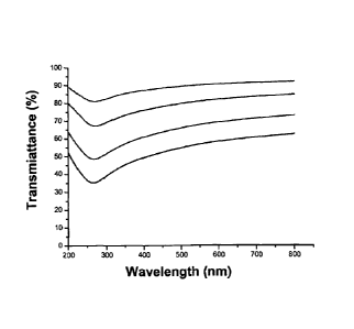
Figure 1 shows the transmittance spectrum of carbon films produced
according to the invention on quartz. The curve corresponds to 30 nm, 22
nm, 12 nm and 4 nm thick carbon films, respectively (from the bottom up).
Figure 2 shows AFM images (2 * 2
pm) of the surface of 4 nm (A)m 12
nm (B) and 30 nm (C) thick carbon films produced according to the invention.
Four sectional plots are given below each image.
Figure 3 shows a high-resolution transmission electron micrograph (HRTEM)
image (A) and a Raman spectrum (B), proofing the graphitic structure of the
carbon films.
Figure 4 shows a solar cell using a carbon film/quartz substrate as an anode.
Figure 5 shows a solar cell using a graphene-structured carbon film as
anode and Au as cathode (A) and the energy level diagram of a
graphene/Ti02/dye/spiro-OMeTAD device (B) as well as the current voltage
characteristics (C).
Figure 6 shows the structures of two preferred discotic precursors, namely of
HBC-PhC12 and of C96.
CA 02684394 2009-10-16
WO 2008/128726
PCT/EP2008/003150
- 12 -
Examples
1. Solutions of discotic precursors C96-C12, HBC-PhC12, oxided graphites
and coal tar pitches, respectively, are coated onto a quartz substrate and the
substrate is then heated to about 1100 C under Ar protection.
2. The thickness of carbon films can be controlled by the concentration of
solution; and the size of film is only limited by the size of substrates.
Depending on the concentration of the solution applied transparent carbon-
based films are obtained having a thickness of 50 nm, 30nm, 13 nm or 3.5
nm.
3. At a wavelength of -700 nm, a carbon film having a thickness of 30 nm,
22 nm, 12 nm and 4 nm has a transmittance of 61%, 72%, 84% and 92%,
respectively (Fig.1). In addition, at a given film thickness, transmittance
was
somewhat dependent upon wavelength with a minimum at -260nm. This
spectral feature is consistent with the carbon soot having a graphitic
structure.
4. The carbon films have a highly smooth surface, free of any large
aggregates, pinholes and cracks, which is important for fabrication of
optoelectronic devices in high quality. The average surface roughness (Ra)
of carbon films with a thickness of 4nm, 12nm and 30nm over a 2 pm * 2 pm
area was around 0.4nm, 0.5nm and 0.7nm respectively (Fig. 2a, 2b and 2c).
5. The as-grown carbon films adhere strongly to substrates. These carbon
films can keep intact even after long time bath sonication in ordinary organic
solvents, and can pass laboratory Scotch-tape test. After immersing the
carbon film/quartz into piranha solution (a mixture of concentrated sulfuric
acid and H202, V:V=7:3) for 48 hours, the conductivity of films keep almost
the same, demonstrating the chemical stability of carbon films against strong
acid and oxidative agent.
6. Structure of graphitic carbon films is confirmed by high-resolution
transmission electron micrograph (HRTEM) (Fig. 3a) and Raman
CA 02684394 2009-10-16
WO 2008/128726
PCT/EP2008/003150
- 13 -
spectroscopy (Fig. 3b). Carbon films show clearly graphitic domains
distributed in the film. The layer-to-layer distance was around 0.35nm, close
to the value of the (002) lattice spacing of graphite. Two typical bands at
approximately 1598cm-1 (G band) and 1300cm-1 (D band) are observed,
assigned to graphitic carbon and disordered carbon, respectively.
7. Sheet resistance of carbon films is in the range of 5 ohm/sq-30 kohm/sq,
dependent of film thickness, precursors, substrates type and heating
condition etc. For example, sheet resistance of 30nm-thick carbon films
grown from C96-C12 on Si02/Si substrates is in a range of 5-50 ohm/sq, and
io that of 10 nm-thick carbon films grown from oxidized graphite is in the
range
of 500-1500 ohm/sq.
8. A solar cell based on a blend of poly(3-hexyl)-thiophene (P3HT) (electron
donor) and phenyl-C61-butyric acid methyl ester (PCBM) (electron acceptor)
is fabricated using a carbon film/quartz as an anode (Fig. 4a, 4b). The
is highest external quantum efficiency (EQE) of around 43% is achieved at a
wavelength of 520nm, comparable to the highest EQE value of 47% for a
reference device, ITO/glass as anode, under similar condition (Figure 4c).
The current-voltage (I-V) characteristic (Fig. 4d) of the carbon film based
device under monochromatic light of 510nm shows a distinct diode behavior.
20 A short-circuit photocurrent density (I.) of 0.052mA/cm2 is observed
with
open-circuit voltage (V.) of 0.13V, calculated filling factor (FF) of 0.23,
and
overall power conversion efficiency of 1.53%. When illuminated with
simulated solar light, the cell gives of 0.36mA/cm2, V. of 0.38V, FF of 0.25
and an efficiency of 0.29%. Obviously, in comparison with ITO based cell,
25 which shows V. of 0.41V, of 1.00mA/cm2, FF of 0.48, and an efficiency of
1.17%. The cell performance is comparable to the ITO based cell.
9. A dye-sensitized solid solar cell based on spiro-OMeTAD (as a hole
transport material) and porous TiO2 (for electron transport) was fabricated
using the graphene-structured carbon film as anode and Au as cathode
30 (Figure 5a). This graphene-structured carbon film was prepared from
exfoliated graphite. Figure 5b shows the energy level diagram of
CA 02684394 2009-10-16
WO 2008/128726
PCT/EP2008/003150
- 14 -
grapheneM02/dye/spiro-OMeTAD/Au device. Since the calculated work
function of graphene is 4.42 eV and the mostly reported work function of
HOPG is 4.5 eV, it is reasonable to presume that the work function of as
prepared graphene-structured carbon film is close to that of FTO electrode
(4.4 eV). The electrons are firstly injected from the excited state of the dye
into the conduction band of TiO2 and then reach the graphene-structured
carbon electrode via a percolation mechanism inside the porous TiO2
structure. Meanwhile, the photooxidized dyes are regenerated by the spiro-
OMeTAD hole conducting molecules. The current-voltage (I-V)
characteristics (Figure 5c, black curve) of the device under illumination of
simulated solar light showed a short-circuit photocurrent density (ls.) of
1.01
mA/cm2 with an open-circuit voltage (V..) of 0.7 V, calculated filling factor
(FF) of 0.36, and overall power conversion efficiency of 0.26 %. For
comparison, an FTO-based cell was fabricated and evaluated with the same
procedure and device structure by replacing graphene film electrode with
FTO. The FTO-based cell gave Is. of 3.02 mA/cm2, V.. of 0.76V, FF of 0.36
and an efficiency of 0.84 % (Figure 5c, red curve). The cell performance is
comparable to the FTO based cell.
10. Using HBC-PhC12 (see the chemical structure shown in Fig. 6) as
zo starting compound, its solution in THF (5 mg/ml) was spin-coated on
quartz
substrate to obtain homogeneous organic film. The film was heat treated in
argon at 400 C for 2 hours and then 600 C for 2h and finally 1100 C for 30
min to obtain carbon film with a thickness of 20 nm. The transparency of the
film at 500 nm is 65%, and the conductivity is 68 S/cm-1.
11. Using C96 (see the chemical structure shown in Fig. 6) as starting
compound, its solution in THF (2.5 mg/ml) was spin-coated on quartz
substrate to obtain homogeneous organic film. The film was heat treated in
argon at 400 C for 2 hours and then 1100 C for 30 min to obtain carbon film
with a thickness of 10 nm. The transparency of the film at 500 nm is 81%,
and the conductivity is 160 S/cm-1.
CA 02684394 2009-10-16
WO 2008/128726
PCT/EP2008/003150
-15-
12. Using C96 (see the chemical structure shown in Fig. 6) as starting
compound, its solution in THF (5 mg/ml) was spin-coated on quartz
substrate to obtain homogeneous organic film. The film was heat treated in
argon at 400 C for 2 hours and then 1100 C for 30 min to obtain carbon film
s with a
thickness of 18 nm. The transparency of the film at 500 nm is 76%,
and the conductivity is 1.60 S/cm-1.
13. Using exfoliated graphite oxide as starting compound, its solution in
water (1.5 mg/ml) was dip-coated on quartz substrate to obtain
homogeneous organic film. The film was heat treated in argon and hydrogen
at 400 C for 30 hours and then 1100 C for 30 min to obtain carbon film with
a thickness of 10 nm. The transparency of the film at 500 nm is 71%, and the
conductivity is 520 S/cm-1.